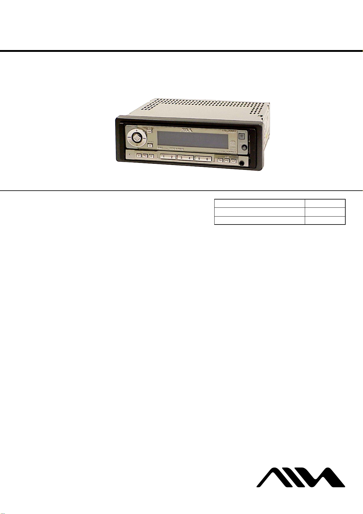
Aiwa CDC-R937 User manual

Ver 1.1 2004. 04
Model Name Using Similar Mechanism NEW
CD Drive Mechanism Type MG-930B-185
Optical Pick-up Name OPTIMA-752B
SERVICE MANUAL
US Model
Canadian Model
CDC-X937
AEP Model
UK Model
CDC-R937
CDC-R937/X937
RADIO SECTION
(FM)
Frequency Range: 87 5 MHz – 108 MHz
Intermediate frequency: 10 7 MHz (CDC-R937)
Usable Sensitivity: 12 7 dBf
50 dB Quieting Sensitivity: 17 2 dBf
IF Rejection: 100 dB
Frequency Response: 30 Hz – 15,000 Hz
S/N Ratio: 67 dB (CDC-R937)
70 dB (CDC-X937)
Stereo Separation: 35 dB at 1 kHz
Alternate Channel Selectivity: 98 dB
Capture Ratio: 3 dB
(AM) (CDC-X937)
Frequency Range: 530 kHz – 1,710 kHz
Usable Sensitivity: 30 µV (30 dB)
(MW) (CDC-R937)
Frequency Range: 531 kHz – 1,602 kHz
Intermediate frequency: 10 71 MHz/450 kHz
Usable Sensitivity: 30 µV (30 dB)
(LW) (CDC-R937)
Frequency Range: 144 kHz – 288 kHz (1 kHz/9 kHz step)
Intermediate frequency: 10 71 MHz/450 kHz
Usable Sensitivity: 30 µV (30 dB)
SPECIFICATIONS
CD SECTION
Frequency Response: 17 Hz – 20 kHz +0/–3 dB
Dynamic Range: More than 92 dB
Channel Separation: More than 60 dB
S/N Ratio: More than 90 dB
Wow/Flutter: Unmeasurable
AUDIO SECTION
Max Power Output: 45 W ×4 channels
AUX IN Input
Input sensitivity (load impedance)AUX IN: 300 mV (10 kΩ)
• The CD section have no adjustment.
Sony Corporation
e Vehicle Company
Published by Sony Engineering Corporation
9-877-344-02
2004D04-1
© 2004. 04
– Continued on next page –
Photo: CDC-R937
FM/AM COMPACT DISC PLAYER
CDC-X937
FM/MW/LW COMPACT DISC PLAYER
CDC-R937

2
CDC-R937/X937
SAFETY-RELATED COMPONENT WARNING!!
COMPONENTS IDENTIFIED BY MARK 0OR DOTTED LINE
WITH MARK 0ON THE SCHEMATIC DIAGRAMS AND IN
THE PARTS LIST ARE CRITICAL TO SAFE OPERATION.
REPLACE THESE COMPONENTS WITH SONY PARTS WHOSE
PART NUMBERS APPEAR AS SHOWN IN THIS MANUAL OR
IN SUPPLEMENTS PUBLISHED BY SONY.
GENERAL
Power-SupplyVoltage: 14 4V (11 to 16 V allowable),
DC, negative ground
Load Impedance: 4 Ω
Tone Control: Bass ±10 dB at 100 Hz,
Treble ±10 dB at 10 kHz
Preamp Output Voltage (load impedance): 2 2 V (10 kΩ)
Installed size: 182 (W) ×53 (H) ×155 (D) mm
(7 1/4 (W) ×2 1/8 (H) ×6 1/8 (D) inches)
SuppliedAccessory: Carrying case (1)
CARD REMOTE CONTROL
Dimensions: Approx 33 (W) ×85 (H) ×7 5 (D) mm
(1 5/16 (W) ×3 3/8 (H) ×5/16 (D) inches)
Weight: Approx 20 g (0 7 oz ) (including battery)
• Specifications and external appearance are subject
to change without notice due to product improvement.
SERVICE NOTES
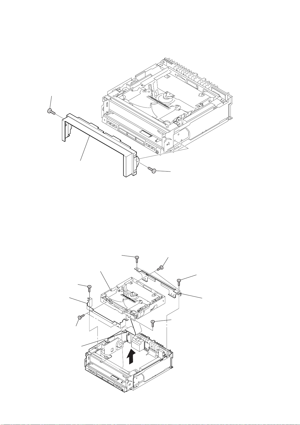
NOTES ON HANDLING THE OPTICAL PICK-UP BLOCK
OR BASE UNIT
The laser diode in the optical pick-up block may suffer electrostatic
breakdown because of the potential difference generated by the
charged electrostatic load, etc. on clothing and the human body.
During repair, pay attention to electrostatic breakdown and also use
the procedure in the printed matter which is included in the repair
parts.
The flexible board is easily damaged and should be handled with
care.
NOTES ON LASER DIODE EMISSION CHECK
The laser beam on this model is concentrated so as to be focused on
the disc reflective surface by the objective lens in the optical pick-
up block. Therefore, when checking the laser diode emission, ob-
serve from more than 30 cm away from the objective lens.
Notes on Chip Component Replacement
•Never reuse a disconnected chip component.
•Notice that the minus side of a tantalum capacitor may be dam-
aged by heat.
CAUTION
Use of controls or adjustments or performance of procedures other
than those specified herein may result in hazardous radiation
exposure.
This compact disc player is classified as a CLASS 1 LASER
product. The CLASS 1 LASER PRODUCT label is located on the
exterior.
CAUTION
Use of controls or adjustments or performance of procedures
other than those specified herein may result in hazardous
radiation exposure.
CDC-X937:
CDC-R937:
ATTENTION AU COMPOSANT AYANT RAPPORT
À LA SÉCURITÉ!!
LES COMPOSANTS IDENTIFIÉS PAR UNE MARQUE 0SUR LES
DIAGRAMMES SCHÉMATIQUES ET LA LISTE DES PIÈCES
SONT CRITIQUES POUR LASÉCURITÉ DE FONCTIONNEMENT.
NE REMPLACER CES COMPOSANTS QUE PAR DES PIÈCES
SONY DONT LES NUMÉROS SONT DONNÉS DANS CE MANUEL
OU DANS LES SUPPLÉMENTS PUBLIÉS PAR SONY.

3
TABLE OF CONTENTS
1. GENERAL
Connections (CDC-X937) ....................................................... 4
Connections (CDC-R937) ....................................................... 5
2. DISASSEMBLY
2-1. Base (Around) ..................................................................... 8
2-2. CD Mechanism Block ......................................................... 8
2-3. Main Board Section ............................................................ 9
2-4. Main Board ......................................................................... 9
2-5. Heat Sink (CT) .................................................................. 10
2-6. Motor (SVX) Assy ............................................................ 10
2-7. Sub Board.......................................................................... 11
2-8. Servo Board....................................................................... 11
2-9. Floating Block Assy .......................................................... 12
2-10. LeverAssy (CD Up Holder CNF) ..................................... 12
2-11. Lever (CD Roller) Sub Assy ............................................. 13
2-12. LeverAssy (CD Holder) ................................................... 13
2-13. Motor (Sled) Sub Assy ...................................................... 14
2-14. Pick-up Sub Assy .............................................................. 14
3. ELECTRICAL ADJUSTMENT.................................... 15
4. DIAGRAMS
4-1. IC Pin Descriptions ........................................................... 16
4-2. Circuit Boards Location .................................................... 19
4-3. Block Diagram –CD Section–........................................... 20
4-4. Block Diagram –Main Section–........................................ 21
4-5. Block Diagram –Front Section–........................................ 22
4-6. Schematic Diagram –CD Mechanism Section–................ 23
4-7. Printed Wiring Boards –CD Mechanism Section–............ 24
4-8. Printed Wiring Board –Main Section– .............................. 26
4-9. Schematic Diagram –Main Section (1/2)–........................ 28
4-10. Schematic Diagram –Main Section (2/2)– ........................ 29
4-11. Printed Wiring Boards –Key Section– .............................. 30
4-12. Schematic Diagram –Key Section–................................... 31
4-13. Printed Wiring Boards –Front Section– ............................ 32
4-14. Schematic Diagrams –Front Section– ............................... 33
4-15. IC Block Diagrams............................................................ 34
5. EXPLODED VIEWS
5-1. Chassis Section ................................................................. 36
5-2. Panel Section ..................................................................... 37
5-3. Front Section ..................................................................... 38
5-4. CD Mechanism Section (1)............................................... 39
5-5. CD Mechanism Section (2)............................................... 40
6. ELECTRICAL PARTS LIST ........................................ 41
CDC-R937/X937

4
CDC-R937/X937 SECTION 1
GENERAL This section is extracted
from instruction manual.
CONNECTIONS (CDC-X937)

5
CDC-R937/X937
CONNECTIONS (CDC-R937)

6
CDC-R937/X937

7
CDC-R937/X937
SECTION 2
DISASSEMBLY
Note : This set can be disassemble according to the following sequence.
2-1. BASE (AROUND)
(Page 8)
2-2. CD MECHANISM BLOCK
(Page 8)
2-7. SUB BOARD
(Page 11)
2-8. SERVO BOARD
(Page 11)
SET
2-14. PICK-UP SUB ASSY
(Page 14)
2-4. MAIN BOARD
(Page 9)
2-5. HEAT SINK (CT)
(Page 10)
2-6. MOTOR (SVX) ASSY
(Page 10)
2-3. MAIN BOARD SECTION
(Page 9)
2-9. FLOATING BLOCK ASSY
(Page 12)
2-10. LEVER ASSY (CD UP HOLDER CNF)
(Page 12)
2-11. LEVER (CD ROLLER) SUB SSY
(Page 13)
2-12. LEVER ASSY (CD HOLDER)
(Page 13)
2-13. MOTOR (SLED) SUB ASSY
(Page 14)

8
CDC-R937/X937
2-2. CD MECHANISM BLOCK
Note : Follow the disassembly procedure in the numerical order given.
2-1. BASE (AROUND)
3
base (around)
2
screw (TH 2.6x4)
1
screw (TH 2.6x4)
6
CON771
qa
CD mechanism block
8
holder (CD mecha
)
5
9
two screws (TH 2.6x4)
0
bracket (CD)
3
screw
(
TH 2.6x4
)
4
screw
(
TH 2.6x4
)
2
screw
(+
PTP 2.6x4
)
1
screw
(+
PTP 2.6x4
)
7
two
screws
(+
PTP 2.6x4
)

9
CDC-R937/X937
2-4. MAIN BOARD
2-3. MAIN BOARD SECTION
2
cover
3
sheet (PWB)
qa
front section
qs
MAIN board section
0
two ground point screws (+PTT 2.6x6)
7
CON721
5
CON701
6
CON702
4
Removal the solder.
brown
black
8
two
screws
(M
2.6x3
)
9
two
screws
(M
2.6x3
)
1
screw
(+
PTP 2.6x4
)
9
MAIN board
7
L chassis
8
R chassis
1
Removal
the solder.
2
Removal the solder.
3
Removal the solder.
4
screw
(+
PTT 2.6x6
)
5
screw
(+
PTT 2.6x6
)
6
screw
(+
PTT 2.6x5
)

10
CDC-R937/X937
2-5. HEAT SINK (CT)
4
heat sink (CT)
1
screw
(+
BTT 2.6x8
)
3
screw
(+
PTT 2.6x8
)
2
two
screws
(+
P 3x12
)
2-6. MOTOR (SVX) ASSY
brown
black
3
motor (SVX) ass
y
6
SENSOR board
4
Removal the solders.
1
screw
(+
PTT 2x3
)
2
screw
(+
PTT 2x3
)
5
screw
(+
PTT 2x3
)

11
CDC-R937/X937
2-8. SERVO BOARD
4
SERVO board
5
PIC2 FLEXIBLE board
1
Removal the solders.
white
gray
red
black
black
red
yellow green
2
screw
(+
PTT 2x3
)
3
two
screws
(M
1.7x5
)
2-7. SUB BOARD
3
SUB board
1
Removal the solders.
black
brown
blue
2
screw
(+
P 1.4x2
)

12
CDC-R937/X937
2-10. LEVER ASSY (CD UP HOLDER CNF)
3
special scre
w
4
tension spring
5
lever assy (CD up holder CNF)
2
leaf spring (roller)
1
screw
(+
P 1.4x2
)
2-9. FLOATING BLOCK ASSY
1
tension spring
2
tension spring
3
tension spring
qd
floating block aasy
4
tension spring
5
tension spring
6
claw
7
claw
8
claw
qa
oil damper
qs
oil damper
9
0

13
CDC-R937/X937
2-12. LEVER ASSY (CD HOLDER)
2
special screw
1
torsion spring
4
lever assy (CD holder)
3
2-11. LEVER (CD ROLLER) SUB ASSY
3
lever (CD roller) sub assy
1
2

14
CDC-R937/X937
2-14. PICK-UP SUB ASSY
2
leaf spring
3
pick-up sub ass
y
1
two
screws
(+
B 1.4x5
)
2-13. MOTOR (SLED) SUB ASSY
2
motor (sled) sub ass
y
1
screw
(+
P 1.7x2
)

15
CDC-R937/X937
RDS Adjustment (CDC-R937 only)
Setting:98 MHz
31 dBµV (EMF)
1 kHz (Modulation Frequency)
45 kHz DEV
Check point: S.METER test point
Adjustment location: SFR101
Specification: 2.0±0.1 V
Procedure: Set to FM98.0 MHz and adjust SFR101 so that the test
point is 2.0±0.2 V.
Adjustment Location:
SECTION 3
ELECTRICAL ADJUSTMENT
TU101
MAIN BOARD (CONDUCTOR SIDE)
IC901
IC151
TP1 S.METER
SFR101
RDS Adjustment
IC501

16
CDC-R937/X937
4-1. IC PIN DESCRIPTIONS
• IC241 TC94A09F-303 (DIGITAL SIGNAL SERVO PROCESSOR) (SERVO BOARD)
Pin No. Pin Name I/O Pin Description
1 – 9 S1 – 9 (OT5 – 13) O LCD segment signal output/Output port Not used. (Open)
10 S10 (OT14/ZDET) O LCD segment signal output/Output port/CD signal Not used. (Open)
11 S11 (OT15/CLCK) O LCD segment signal output/Output port/CD signal Not used. (Open)
12 S12 (OT16/DATA) O LCD segment signal output/Output port/CD signal Not used. (Open)
13 S13 (OT17/SFSY) O LCD segment signal output/Output port/CD signal Not used. (Open)
14 S14 (DT18/LRCK) O LCD segment signal output/Output port/CD signal Not used. (Open)
15 P8-0 (S15/BCK) I/O I/O port/LCD segment signal output/CD signal Not used. (Open)
16 P8-1 (S16/AOUT) I/O I/O port/LCD segment signal output/CD signal Not used. (Open)
17 P8-2 (S17/MBOV) I/O I/O port/LCD segment signal output/CD signal Not used. (Open)
18 P8-3 (S18/IPF) I/O I/O port/LCD segment signal output/CD signal Not used. (Open)
19 MVDD1 — Power supply pin (+5 V)
20 MVSS — Ground pin
21 LMT SW I Limit switch signal input
22 P1-1 (K1) I Key signal input
23 P1-2 (K2) I Key signal input
24 SW3 I Key signal input
25 SRQ I CDS SRQ signal input
26 LM CONT O Loading motor speed control signal output
27 P3-2 (ADIN2) I/O I/O port/AD analog voltage signal input Not used. (Open)
28 P3-3 (ADIN3) O Mute signal output
29 P4-0 (BUZR/AD4) I/O I/O port/AD analog voltage signal input/buzzer signal output Not used. (Open)
30 DATA IN I CDS serial data signal input
31 DATA OUT O CDS serial data signal output
32 CLOCK I/O CDS serial clock signal input/output
33 P2-0/EMPH I/O Emphasis signal input/output
34 P2-1/HSO I/O I/O port/1 bit DAC input Not used. (Open)
35 P2-2/LRCK I/O I/O port/1 bit DAC input Not used. (Open)
36 P2-3/DATA I/O I/O port/1 bit DAC input Not used. (Open)
37 IN1/BCK I Input port/1 bit DAC input Connect to ground.
38 TESTC I Test mode control input Not used. (Open)
39 DT19 (/HSO) O Output port/CD control signal output Not used. (Open)
40 DT20 (SPCK) O Output port/CD control signal output Not used. (Open)
41 DT21 (SPDA) O Output port/CD control signal output Not used. (Open)
42 DT22 (COFS) O Output port/CD control signal output Not used. (Open)
43 DOUT O Digital out signal output Not used. (Open)
44 SBSY O Sub code block sync signal output Not used. (Open)
45 SBOK O Sub code Q data signal output Not used. (Open)
46 VDD1 — Power supply pin (+5 V)
47 VSS1 — Ground pin
48 P2VREF — PLL 2 voltage reference pin
49 PDO I EFM/PLCK signal difference error signal input
50 TMAX I TMAX detect signal input
51 LPFN I Inversion signal input of amplifier for lowpass filter
52 LPFO O Signal output of amplifier for lowpass filter
53 PVREF I PLL voltage reference input
54 VCOF O VCO filter signal output
55 AVSS — Ground pin
56 SLCO O DAC signal output
57 RFI I RF signal input
58 AVDD — Power supply pin (+5 V)
59 RFCT I RFRP signal center level input
SECTION 4
DIAGRAMS

17
CDC-R937/X937
Pin No. Pin Name I/O Pin Description
60 RFZI I RFRP zero-closs signal input
61 RFRP I RFRP ripple signal input
62 FEI I Focus error signal input
63 SBAD I Sub beam addition signal input
64 TEI I Tracking error signal input
65 TEZI I Tracking error zero-closs signal input
66 FOO O Focus equalizer signal output
67 TRO O Tracking equalizer signal output
68 VREF — Analog reference power supply pin
69 RFGC O RF amplitude adjustment control signal output
70 TEBC O Tracking balance control signal output
71 FMO O Focus equalizer signal output
72 DMO O Disc equalizer signal output
73 2VREF — Analog reference power supply pin
74 SEL O APC circuit on/off signal output
75 VDD2 — Power supply pin (+5 V)
76, 77 VSS2, XVSS — Ground pin
78 XI I Crystal oscillator input for CD
79 XO O Crystal oscillator output for CD
80 XVDD — Power supply pin (+5 V)
81 DVSR — Ground pin
82 RO O R channel data clock wise signal output
83 DVRR — R channel reference voltage pin
84 DVDD — Power supply pin
85 DVRL — L channel reference voltage pin
86 LO O L channel data clock wise signal output
87 DVSL — Ground pin
88 TESTM I Ground pin
89 IN2/(VPP) I Ground pin
90 RESET I System reset signal input
91 /HOLD I Hold mode control signal input
92 CS I External interruption signal input
93 MXO O Not used. (Open)
94 MXI I Ground pin
95 MVSS2 — Ground pin
96 MVDD2 — Power supply pin (+5 V)
97 – 100 COM1 – 4 (OT1 – 4) O Not used. (Open)

18
CDC-R937/X937
• IC901 µPD178078GF-588-3BA (SYSTEM CONTROL) (MAIN BOARD) (CDC-R937)
• IC901 µPD178076GF-571-3BA (SYSTEM CONTROL) (MAIN BOARD) (CDC-X937)
Pin No. Pin Name I/O Pin Description
1BATT IN I Battery signal input
2DFP IN I Front panel with/without detect signal input
3LCD DI I LCD serial data signal input
4LCD DO O LCD serial data signal output
5LCD CLO O LCD sync clock signal output
6LCD CE O LCD driver CE signal output
7 BBE SW1 O BBE on/off select signal output
8CDS DI I CDS serial data signal input
9CDS DO O CDS serial data signal output
10 CDS CLO O CDS sync clock signal output
11 – 15 NC O Not used. (Open)
16 BBE SW2 O BBE effectiveness select signal output
17 NC O Not used. (Open)
18 EVOL CLO O Clock signal output to electronic volume
19 EVOL DO O Serial data signal output to electronic volume
20 EVOL CE O CE signal output to electronic volume
21 LOC/DX O LOC/DX select signal output
22 DSSA CONT O DSSA control signal output “H”: DSSA L/R
23 ACC DET I Power supply overvoltage detect signal input
24 PH MUTE I External mute control signal input
25 LEV.IND. I Level signal input
26 TEST — CDS test mode pin
27 AVDD — Power supply pin (+5 V)
28 – 30 KEY1 – KEY3 I A/D key signal input
31 FM/AM S M I CDC-R937: RDS AF signal input CDC-X937: FM/AM S meter signal input
32 AVSS — Ground pin
33 REG CPU — Regulator for CPU power supply
34 VDD — Power supply pin (+5 V)
35 REG OSC — Regulator for oscillator circuit
36 X OUT O System clock oscillator output (6.3 MHz)
37 X IN I System clock oscillator input (6.3 MHz)
38 GND0 — Ground pin
39 IF REQ O IF count signal request output
40 GND2 — Ground pin
41 AM IF I AM IF count signal input
42 FM IF I FM IF count signal input
43 VDD PLL — Power supply pin for PLL (+5 V)
44 FM OSC I FM local oscillator signal input
45 AM OSC I AM local oscillator signal input
46 GND PLL — Ground pin for PLL
47 EO 0 O Error out signal output from charge pomp
48 EO 1 O Error out signal output from charge pomp
49 IC — Not used. (Connect to ground.)
50 RESET I System reset signal input
51 RDS CL IN I CDC-R937: RDS clock signal input CDC-X937: Not used. (Open)
52 ACC IN I ACC on/off detect signal input
53 RMT IN I Remote control signal input
54 ST IN/SD IN I FM receive stereo signal input
55 ST O CDC-X937: FM receive forced monaural change over signal output
CDC-R937: Not used. (Open)
56 ST BY MUTE O ST-BY mute control signal output to power IC

19 19
CDC-R937/X937
4-2. CIRCUIT BOARDS LOCATION
Pin No. Pin Name I/O Pin Description
57 POWER CONT O Power control signal output
58 RDS DI I CDC-R937: RDS serial data signal input CDC-X937: Not used. (Open)
59 BEEP O Beep signal output
60 MUTE O Audio mute control signal output
61 LED O LED on/off control signal output (for CD window LED)
62, 63 NC O Not used. (Open)
64 RDS MODE O RDS mode signal output “H”: RDS AF
65 POWER MUTE O Mute control signal output to power IC
66 FM BAND O Band (FM) select signal output
67 AM BAND O Band (AM) select signal output
68 NC O Not used. (Open)
69 ILLUM CONT 1 O Panel illumination color change over signal output “H”: Blue, “L”: Red
70 ILLUM CONT 2 O Panel illumination color change over signal output “H”: Red, “L”: Blue
71 MI-1 I Diode matrix input for initial setting
72 MI-2 I Diode matrix input for initial setting
73 MI-3 I Diode matrix input for initial setting Not used. (Open)
74 MO-1 O Diode matrix output for initial setting Not used. (Open)
75 MO-2 O Diode matrix output for initial setting
76 MO-3 O Diode matrix output for initial setting
77 MO-4 O Diode matrix output for initial setting
78 AUX SW I AUX detection signal input
79 CDS SREQ I CDS S-REQ signal input
80 LAMP CONT O Lamp control signal output
81 TEST CD O Not used. (Open)
82 GND1 — Ground pin
83 TEST MF O Not used. (Open)
84, 85 PANCON 1, 2 O Panel open/close control signal output
86 SW1 I Disc detection switch 1 signal input
87 SW2 I Disc detection switch 2 signal input
88 SW3 I Not used. (Open)
89 PANEL SW I M-FLAP DFP open/close control signal input
90 MF CONT O Power supply control signal output for panel operation
91 SEN 1 I Position detection (photo sens) signal input for panel open/close
92 SEN 2 I Position detection (lilit sw) signal input for panel open/close
93 LMT SW O Not used. (Open)
94 CDS RESET O CDS reset signal output
95 CDS SLEEP O CDS sleep signal output
96 CDS CS O CDS CS signal output
97 (CDS STOP) O Not used. (Open)
98 RADIO CONT O Radio control signal output
99 VDD PORT — Power supply pin (+5 V)
100 GND PORT — Ground pin
KEY board
LED board
INDICATOR board
SUB board
SENSOR board
SERVO board
MAIN board
AUX board
tuner uni
t
(TU101)

2020
CDC-R937/X937
4-3. BLOCK DIAGRAM — CD SECTION —
(Page 21)
25
24
22
20
16
17
15
14
13
11
10
2
26
57
60
59
62
86
82
63
64
65
70
74
69
33
9
8
4
7
6
5
FOCUS
COIL
DRIVE
LD
DRIVE
Q221
TRACKING
COIL
DRIVE
SPINDLE
MOTOR
DRIVE
5V
REG.
8
9
20
M2
(SPINDLE) M
M1
(SLED/LOADING) M
-
+
+
-
FOCUS
COIL
TRACKING
COIL
VIN3
VIN3G
VIN4
VIN4G
VIN2
VIN2G
VIN1
REG IN
VIN1G
MUTE
VO3+
VO3-
VO4+
VO4-
VO2+
VO2-
VO1+
VO1-
REG
OUT
FOCUS/TRACKING COIL DRIVE,
SLED/SPINDLE/LOADING MOTOR DRIVE,
IC201
6
7
4
5
13
15
25
16
14
19 +5V REG
Q201
24
23
17
18
S3
(CHUCH)
S2
(DISC IN2)
S1
(DISC IN1)
S4
(LIMIT)
CD+5V
VC
1
2
3
4
5
6
7
8
9
10
11
13
12
15
14
FPI
RFI
RFZI
FEI
RFCT
61 RFRP
SBAD
TEI
TEZI
TEBC
SEL
RFGC
P2-O/EMPH
78 XI
79 XO
66 FOO
67 TRO
28 P3-3(ADIN3)
72 DMO
26 LM CONT
71 FMO
TPI
TNI
FNI
MDI
LDD
19 VRO
RFGO LO
RO
RFRPIN
RFCT
RFRP
FEO
FEN
SBAD
TEO
TEN
TEB
SEL
RFGC
GVSW
VC
10
11
X241
16.9344MHz
DIGITAL SIGNAL SERVO PROCESSOR
IC241
RF AMP
IC221
23
P1-2(K2)
24
SW3
22
P1-1(K1)
CDS SRQ
SW1
CDS DMSCD
CDS DCDMS
CDS CLO
CDS CS
RESET
CD R
CD L
21
LIMIT SW
CD+5V
CD+8V
OPTICAL PICK-UP
BLOCK
MAIN
SECTION
A
SLED/
LOADING
MOTOR
DRIVE
SPEED
CONTROL
Q202
90
92
RESET
CS
32
31
CLOCK
SRQ
30
25
DATA OUT
DATA IN
SW2
• Signal path
:CD
Other manuals for CDC-R937
1
This manual suits for next models
1
Table of contents
Other Aiwa CD Player manuals
Popular CD Player manuals by other brands

APART
APART BGM3000 manual

IMG STAGE LINE
IMG STAGE LINE CD-70DJ B instruction manual

NAD
NAD 5240 Instructions for installation and operation

Cayin
Cayin CS-100CD quick start guide

Philips
Philips Soundmachine AZ100B quick start guide

Sony
Sony CDX-RA700 - Motorized Synchro-flip Detachable... operating instructions