Aiwa 6ZG-1S User manual

•BASIC CD MECHANISM:3ZG-2 E2 •TYPE:English
CD MECHANISM
6ZG-1S
6ZG-1S2
6ZG-1S3
S/M Code No.09-984-249-90T
This mechanism has various derivation. Derivation name is indicated by
the Service Manual for eath model.
DERIVATION NAMEBASIC NAME
6ZG-1S
6ZG-1S3 D SH
6ZG-1S2 D SH
DSH
jomi

2
TABLE OF CONTENTS
PROTECTION OF EYES FROM LASER BEAM DURING SERVICING/
Precaution to replace Optical block......................................................................................................... 3
SUFFIX NOTE ........................................................................................................................................ 4
TRANSISTOR ILLUSTRATION .............................................................................................................. 5
DISASSEMBLY INSTRUCTIONS........................................................................................................ 6-8
6ZG-1S
ELECTRICAL MAIN PARTS LIST ................................................................................................................9, 10
BLOCK DIAGRAM ......................................................................................................................................11, 12
WIRING.......................................................................................................................................................13, 14
SCHEMATIC DIAGRAM .............................................................................................................................15, 16
IC DESCRIPTION........................................................................................................................................17-20
IC BLOCK DIAGRAM .......................................................................................................................................21
TEST MODE .....................................................................................................................................................22
MECHANICAL EXPLODED VIEW 1/1..............................................................................................................23
MECHANICAL PARTS LIST 1/1.......................................................................................................................24
CD MECHANISM EXPLODED VIEW/LIST (3ZG-1 E2) ...................................................................................25
6ZG-1S2
ELECTRICAL MAIN PARTS LIST ..............................................................................................................26, 27
IC BLOCK DIAGRAM .......................................................................................................................................29
BLOCK DIAGRAM ......................................................................................................................................30, 31
WIRING.......................................................................................................................................................32, 33
SCHEMATIC DIAGRAM .............................................................................................................................34, 35
IC DESCRIPTION.......................................................................................................................................36, 37
6ZG-1S3
ELECTRICAL MAIN PARTS LIST ..............................................................................................................38, 39
BLOCK DIAGRAM ......................................................................................................................................41, 42
WIRING.......................................................................................................................................................43, 44
SCHEMATIC DIAGRAM .............................................................................................................................45, 46
TEST MODE .....................................................................................................................................................47
USE MODEL LIST ................................................................................................................................ 48
jomi

3
PROTECTION OF EYES FROM LASER BEAM DURING SERVICING
VAROITUS!
Laiteen Käyttäminen muulla kuin tässä käyttöohjeessa mainit-
ulla tavalla saattaa altistaa käyt-täjän turvallisuusluokan 1 ylit-
tävälle näkymättömälle lasersäteilylle.
VARNING!
Om apparaten används på annat sätt än vad som specificeras i
denna bruksanvising, kan användaren utsättas för osynling
laserstrålning, som överskrider gränsen för laserklass 1.
Caution: Invisible laser radiation when
open and interlocks defeated avoid expo-
sure to beam.
Advarsel:Usynling laserståling ved åbning,
når sikkerhedsafbrydere er ude af funktion.
Undgå udsættelse for stråling.
CAUTION
Use of controls or adjustments or performance of procedures
other than those specified herein may result in hazardous
radiation exposure.
ATTENTION
L'utilisation de commandes, réglages ou procédures autres que
ceux spécifiés peut entraîner une dangereuse exposition aux
radiations.
ADVARSEL!
Usynlig laserståling ved åbning, når sikkerhedsafbrydereer ude
af funktion. Undgå udsættelse for stråling.
This Compact Disc player is classified as a CLASS 1 LASER
product.
The CLASS 1 LASER PRODUCT label is located on the rear
exterior.
This set employs laser. Therefore, be sure to follow carefully the
instructions below when servicing.
WARNING!
WHEN SERVICING, DO NOT APPROACH THE LASER EXIT
WITH THE EYE TOO CLOSELY. IN CASE IT IS NECESSARY TO
CONFIRM LASER BEAM EMISSION. BE SURE TO OBSERVE
FROM A DISTANCE OF MORE THAN 30cm FROM THE
SURFACE OF THE OBJECTIVE LENS ON THE OPTICAL
PICK-UP BLOCK.
CLASS 1
KLASSE 1
LUOKAN 1
KLASS 1
LASER PRODUCT
LASER PRODUKT
LASER LAITE
LASER APPARAT
Precaution to replace Optical block
(KSS-213F)
1) After the connection, remove solder shown in
the right figure.
Body or clothes electrostatic potential could ruin
laser diode in the optical block. Be sure ground
body and workbench, and use care the clothes
do not touch the diode.
jomi

4
This is the SERVICE MANUAL for the BASIC CD MECHANISM of BASIC NAME: 6ZG-
1. This BASIC NAME includes the following models as shown under the SUFFIX
name: DERIVATION NAME. Please use this manual with the separate SERVICE
MANUAL for DERIVATION NAME.
BASIC CD MECHANISM: 6ZG-1 DSH
SUFFIX
(DERIVATION NAME)
BASIC NAME: 6ZG-1S (SONY IC HIGH END MODEL)
6ZG-1S2 (The 2nd SONY IC MODEL)
6ZG-1S3 (The 3rd SONY IC MODEL)
DERIVATION NAME
D: Digital output function
SH: Pick up equipped with shutter
BASIC NAME DERIVATION NAME
6ZG-1S D SH — — — —
6ZG-1S2 D SH — — — —
6ZG-1S3 D SH — — — —
jomi

5
TRANSISTOR ILLUSTRATION
2SA1015
2SC2001
2SD2172
2SD655
2SA1235
2SC2412
2SC2712
DTA114EK
DTC114EK
DTC114TK
DTC123JK
DTC143TK
2SA933S
DTC114ES 2SB1329
E C B E C B BE
C
B C E
jomi

6
1. How to replace PICK UP.
1) Open the TRAY.
Push the stopper to arrow direction and release half of
the SHAFT SLED.
2) Turn GEAR MAIN CAM to the counterclockwise
(arrow “a”) direction, and lift up CD mechanism. (Fig-1)
3) Remove SHAFT SLED.
4) CD mechanism in down position, replace PICK UP.
5) Lift up CD mechanism (Fig-1), and Reassemble the
SHAFT SLED.
2. How to remove the 5CD CHANGER BLOCK
(Fig-2)
1) Remove the two FFC of the CD circuit board, and
remove the five SCREWS.
2) Lift 5 CD CHANGER BLOCK from behind, and
remove it. (5CD CHANGER BLOCK can be removed
even if PANEL TRAY is not removed.)
DISASSEMBLY INSTRUCTIONS
STOPPER
GEAR MAIN CAM °
SHAFT SLED
PICKUP
FFC
FFC SCREW
5CD CHANGER BLOCK
LIFT UP
Fig-1
Fig-2
jomi

7
3. The disassemble and reassemble the TRAY
3-1. Disassembling procedure.
1) Push the PLATE GEAR’S Boss at the bottom part of
CHAS MECHA strongly to the outside (arrow “b”
direction). (Fig-3)
(Confirm that TRAY appears a little in the front.)
2) Draw TRAY to the open position.
3) Remove FFC, and push the two LEVERS at both side of
the CHAS MECH to remove TRAY. (Fig-4)
3-2. Reassembling procedure.
1) Confirm that LEVER TRAY is at the most right position
and check for the CD Mechanism to be in the down
position. (Fig-5)
2) Push in the TRAY along the rail of the CHAS MECHA.
5CD CHANGER BLOCK
BOSS
b
FFC
Fig-3
LEVER TRY
TRAY
FFC
Fig-5 Fig-6
Fig-4
LEVER
LEVER
TRAY
3) After TRAY is half closed and FFC is put in, it can enter
by force until the end of TRAY closed. (Fig-6)
jomi

8
4. How to reassemble the TURN TABLE. (Fig-7)
1) Push LEVER TT in the direction of “C”, and put in the
TURN TABLE 5CD. (Fig-7)
After reassembly, one of the TURN TABLE DISC
TRAY (can be either one of the five disc trays) must be
aligned with TURN TABLE 5CD. (Fig-8)
That is, having no gap difference between the TURN
TABLE 5CD and the TRAY 5CD.
* When reassembling the TURN TABLE 5CD, it is
acceptable facing any CD number (1-5).
ALIGN
TURN TABLE 5CD
TRAY 5CD
Fig-7 Fig-8
CLEVER TT
jomi

9
MODEL NO. 6ZG-1S
REF. NO PART NO. KANRI DESCRIPTION
NO.
REF. NO PART NO. KANRI DESCRIPTION
NO.
ELECTRICAL MAIN PARTS LIST
IC
87-A20-547-010 C-IC,CXA1992AR
87-A20-546-010 C-IC,CXD2589Q
87-A20-592-040 C-IC,M51943 AML
87-070-305-010 IC,BA6897S
87-001-982-010 IC,TA7291S
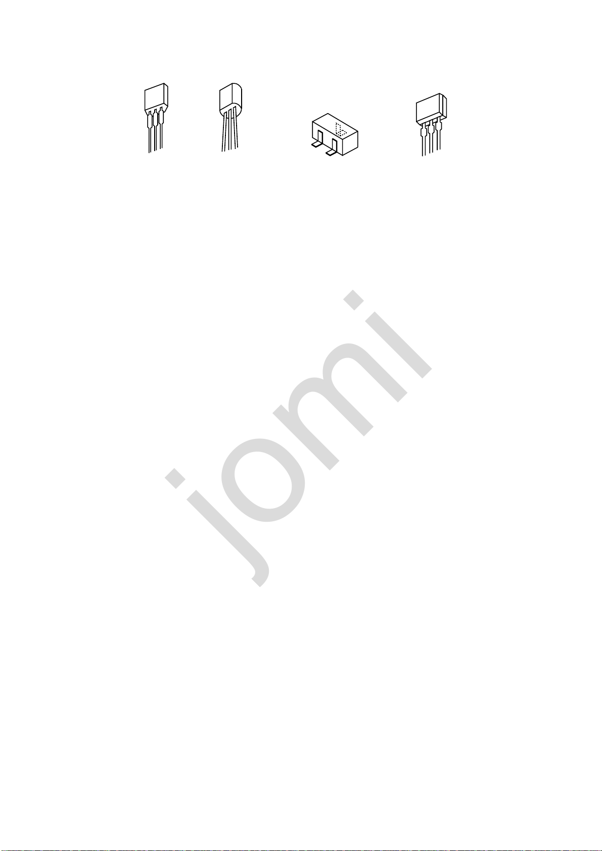
TRANSISTOR
89-406-555-080 TR,2SD655 (0.5W)
87-026-463-080 TR,2SA933S (0.3W)
89-421-722-380 TR,2SD2172V/W
89-320-011-080 TR,2SC2001 (15W)
87-026-223-080 TR,DTC143TK
89-110-155-080 TR,2SA1015(0.4W)
87-026-608-080 C-TR,DTC 123 JK
89-327-125-080 CHIP TR,2SC2712GR<D>
DIODE
87-020-465-080 DIODE,1SS133 (110MA)
CD MAIN C.B
C1 87-010-196-020 C-CAP,S 0.1-25 F
C2 87-010-260-080 CAP, ELECT 47-25V
C4 87-010-197-020 C-CAP,S 0.01-25 B
C101 87-010-263-040 CAP,E 100-10
C102 87-010-178-020 C-CAP,S 1000P-50 B
C103 87-010-550-040 CAP,E 100-6.3 GAS
C104 87-010-182-020 C-CAP,S 2200P-50 B
C105 87-010-198-020 C-CAP,S 0.022-25 B
C106 87-016-081-020 C-CAP,S 0.1-16 RK
C107 87-016-081-020 C-CAP,S 0.1-16 RK
C108 87-016-081-020 C-CAP,S 0.1-16 RK
C109 87-010-497-040 CAP,E 4.7-35 GAS
C110 87-010-198-080 CAP, CHIP 0.022
C111 87-010-197-020 C-CAP,S 0.01-25 B
C112 87-010-402-040 CAP,E 2.2-50 SME
C113 87-010-382-040 CAP,E 22-25 SME
C114 87-010-213-020 C-CAP,S 0.015-25 B
C115 87-010-263-040 CAP,E 100-10
C116 87-010-197-020 C-CAP,S 0.01-25 B
C117 87-016-369-020 C-CAP,S 0.033-25 B K
C118 87-010-197-020 C-CAP,S 0.01-25 B
C119 87-016-369-020 C-CAP,S 0.033-25 B K
C120 87-010-197-020 C-CAP,S 0.01-25 B
C121 87-010-494-040 CAP,E 1-50 GAS
C122 87-010-154-020 C-CAP,S 10P-50 CH
C123 87-010-154-020 C-CAP,S 10P-50 CH
C124 87-010-154-020 C-CAP,S 10P-50 CH
C125 87-010-596-020 C-CAP,S 0.047-16 RK
C126 87-010-596-020 C-CAP,S 0.047-16 RK
C127 87-012-140-020 C-CAP,S 470P-50 CH
C128 87-010-596-020 C-CAP,S 0.047-16 RK
C129 87-010-198-020 C-CAP,S 0.022-25 B
C130 87-016-081-020 C-CAP,S 0.1-16 RK
C131 87-010-550-040 CAP,E 100-6.3 GAS
C132 87-010-550-040 CAP,E 100-6.3 GAS
C133 87-012-158-020 C-CAP,S 390P-50 J CH
C150 87-010-145-020 C-CAP,S 1P-50 C CH
C202 87-010-596-020 C-CAP,S 0.047-16 RK
C203 87-010-188-020 C-CAP,S 6800P-50 B
C204 87-012-156-020 C-CAP,S 220P-50 CH
C205 87-018-134-080 CAPACITOR,TC-U 0.01-16
C206 87-010-400-040 CAP,E 0.47-50
C207 87-010-197-020 C-CAP,S 0.01-25 B
C208 87-010-318-020 C-CAP,S 47P-50 CH<D>
C209 87-012-154-020 C-CAP,S 150P-50 J CH GRM
C210 87-012-154-020 C-CAP,S 150P-50 J CH GRM
C211 87-010-176-020 C-CAP,S 680P-50 J SL
C212 87-010-176-020 C-CAP,S 680P-50 J SL
C213 87-010-382-040 CAP,E 22-25 SME<D>
C213 87-010-401-040 CAP,E 1-50 SME
C214 87-010-382-040 CAP,E 22-25 SME<D>
C214 87-010-401-040 CAP,E 1-50 SME
C215 87-010-318-020 C-CAP,S 47P-50 CH
C216 87-010-318-020 C-CAP,S 47P-50 CH
C217 87-010-380-040 CAP,E 47-16 SME
C218 87-010-197-020 C-CAP,S 0.01-25 B
C219 87-010-196-020 C-CAP,S 0.1-25 F
C220 87-010-370-040 CAP,E 330-6.3 SME
C221 87-010-197-020 C-CAP,S 0.01-25 B
C222 87-010-186-020 C-CAP,S 4700P-50 B
C223 87-016-081-020 C-CAP,S 0.1-16 RK
C228 87-018-209-080 CAP, CER 0.1-50V
C230 87-016-081-020 C-CAP,S 0.1-16 RK
C231 87-018-209-080 CAP, CER 0.1-50V
C401 87-010-403-080 CAP, ELECT 3.3-50V
C402 87-010-403-040 CAP,E 3.3-50 SME
C501 87-016-459-040 CAP,E 470-10 SMG
C502 87-010-197-020 C-CAP,S 0.01-25 B
C503 87-010-263-040 CAP,E 100-10
C504 87-010-196-020 C-CAP,S 0.1-25 F
C505 87-010-196-020 C-CAP,S 0.1-25 F
C506 87-010-196-020 C-CAP,S 0.1-25 F
C507 87-010-196-020 C-CAP,S 0.1-25 F
C508 87-016-459-040 CAP,E 470-10 SMG
C509 87-010-196-020 C-CAP,S 0.1-25 F
C510 87-010-196-020 C-CAP,S 0.1-25 F
C601 87-010-197-020 C-CAP,S 0.01-25 B
C602 87-016-251-040 CAP,E 220-16 SMG
C603 87-010-196-020 C-CAP,S 0.1-25 F
C701 87-010-322-020 C-CAP,S 100P-50 CH
C702 87-010-318-020 C-CAP,S 47P-50 CH
C703 87-010-318-020 C-CAP,S 47P-50 CH
C705 87-010-178-020 C-CAP,S 1000P-50 B
C706 87-018-199-080 CAP, CER 3300P
C901 87-010-260-040 CAP,E 47-25 SME<D>
C902 87-010-196-020 C-CAP,S 0.1-25 F<D>
CN3 86-ZG1-609-010 CONN ASSY,6P
FB1 87-003-223-080 FERRITE BEAD BL02RN2
FB2 87-003-223-080 FERRITE BEAD BL02RN2
FB3 87-003-223-080 FERRITE BEAD BL02RN2
FC1 86-ZG1-605-010 CABLE,FFC 16P
FC2 86-ZG1-608-010 CABLE,FFC 8P
L28 83-XM1-617-080 C-COIL,BK2125HM601
L41 83-XM1-617-080 C-COIL,BK2125HM601
L101 87-003-102-080 COIL, 10UH
L201 87-003-102-080 COIL, 10UH
LED901 87-A40-123-010 LED,SLZ-8128A-01-B<D>
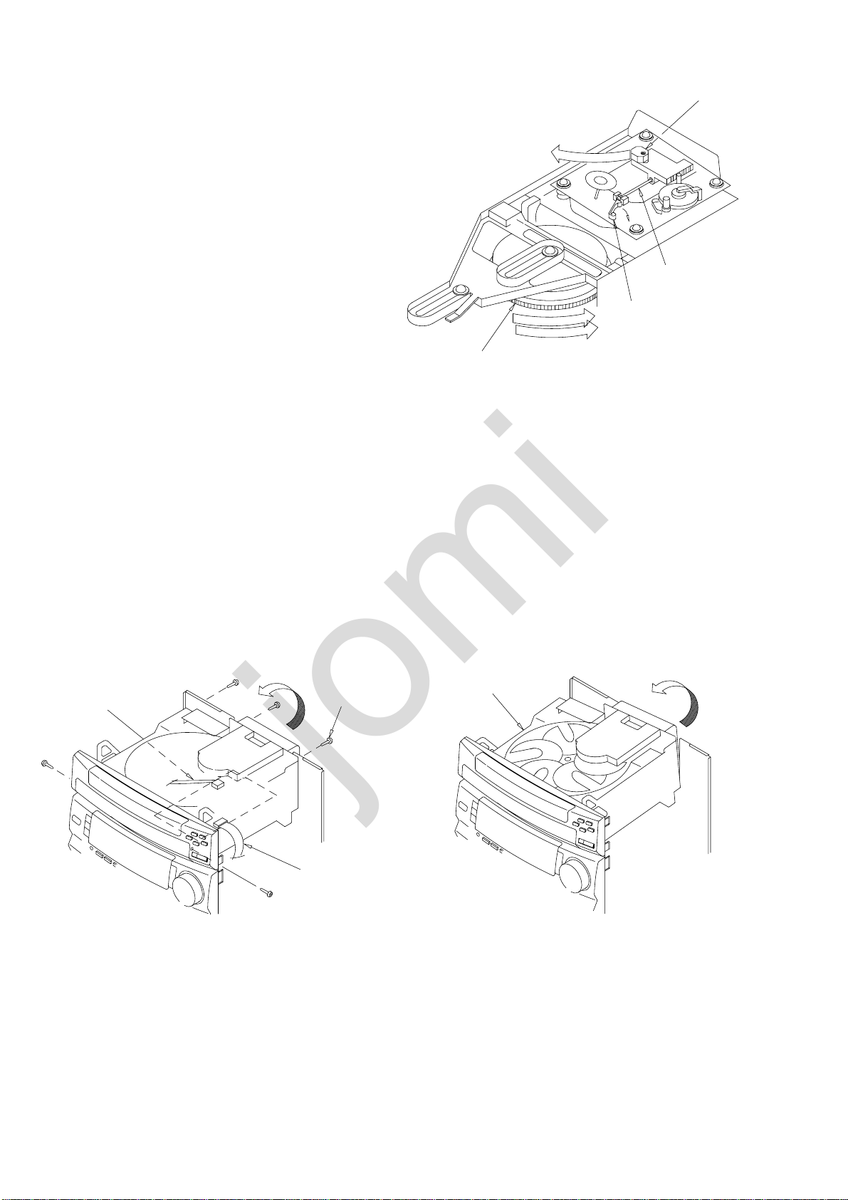
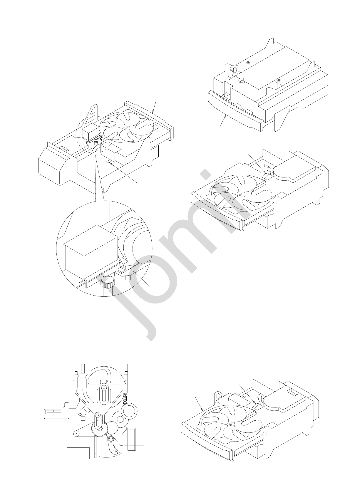
M601 87-045-305-010 MOTOR, RF-500TB DC-5V (2MA)
!
PR1 87-026-689-080 PROTECTOR,1A 60V 491
R101 87-022-363-020 C-RES,S 68K-1/10W F
R102 87-022-363-020 C-RES,S 68K-1/10W F
R103 87-022-363-020 C-RES,S 68K-1/10W F
R104 87-022-363-020 C-RES,S 68K-1/10W F
R105 87-022-365-020 C-RES,S 100K-1/10W F
R106 87-022-365-020 C-RES,S 100K-1/10W F
R420 87-029-060-080 RES,FUSE 33-1/4 W
S601 87-036-109-010 PUSH SWITCH
S602 87-036-109-010 PUSH SWITCH
S603 87-036-109-010 PUSH SWITCH
X201 87-A70-046-010 VIB,XTAL 16.934MHZ
LED C.B
LED701 87-017-733-080 LED,SEL1250SM
LED702 87-017-350-080 LED,SEL1550CM
jomi

10
REF. NO PART NO. KANRI DESCRIPTION
NO.
LED703 87-017-733-080 LED,SEL1250SM
T-T C.B
C411 87-018-214-080 CAP TC U 0.1-50F
LED411 87-070-288-010 LED,GL380
M401 87-A90-036-010 MOT ASSY,RF-300CA-11
PS401 87-A90-156-010 SNSR,SG-240
Q411 87-A30-031-010 P-TR,PT380F
S401 87-036-109-010 PUSH SWITCH
• Regarding connectors, they are not stocked as they are not the initial order items.
The connectors are available after they are supplied from connector manufacturers upon the order is received.
W
Resistor Code
1/16W
1/10W
1/8W
1608
2125
3216
5%
5%
5%
CJ
CJ
CJ
L
1.6
2
3.2
W
0.8
1.25
1.6
t
0.45
0.45
0.55
108
118
128
88
t
L
/ CHIP RESISTOR PART CODE
Chip Resistor Part Coding
Figure
Value of resistor
Chip resistor
Wattage Type Tolerance Symbol / Diamensions (mm)
/ Form Resistor Code : A
jomi

1211
BLOCK DIAGRAM
RF
jomi

1413
WIRING
12345678910 11 12 13 14
A
B
C
D
E
F
G
H
I
J
jomi

1615
SCHEMATIC DIAGRAM
KSS-213F
jomi

17
Output terminal for focus error amplifier. Internally connected to window comparator
input for bias condition.
Input terminal for focus error.
Capacitor connection terminal for time constant used when there is defect.
This pin is connected to GND via capacitor when high frequency gain of the focus
servo is attenuated.
This is a pin where the time constant is externally connected to raise the low frequency
gain of the focus servo.
Focus drive output.
Focus amplifier inverted input pin.
This is a pin where the time constant is externally connected to generate the focus
search waveform.
This is a pin where the selection time constant is externally connected to set the
tracking servo the high frequency gain.
This is a pin where the selection time constant is externally connected to set the
tracking high frequency gain.
Pin for setting peak of the phase compensator of the focus tracking.
Tracking amplifier inverted input pin.
Tracking drive output.
Sled amplifier non-inverted input pin.
Sled amplifier inverted input pin.
Sled drive output.
The current which determines height of the focus search, track jump and sled kick is
input with external resistance connected.
Power supply.
“L” setting starts sled disorder-prevention circuit. (Not pull-up resistance)
Clock input for serial data transfer from CPU. (No pull-up resistance)
Latch input from CPU. (No pull-up resistance)
Serial data input from CPU. (No pull-up resistance)
Reset system at “L” setting. (No pull-up resistance)
Signal output for track number counting.
FZC, DFCT1, TZC, BALH, TGH, FOH, or ATSC is output depending on the
command from CPU.
DFCT2, MIRR, BALL, TGL or FOL is output depending on the command from CPU.
Output terminal for focus OK comparator.
Input pin where the DEFECT bottom hold output is capacitance coupled.
DEFECT bottom-hold output terminal. Internally connected to interruption comparator
input.
Connection terminal for DEFECT bottom-hold capacitor.
Connection terminal for MIRR hold-capacitor.
Anti-reverse input terminal for MIRR comparator.
FEO
FEI
FDFCT
FGD
FLB
FE_O
FEM
SRCH
TGU
TG2
FSET
TA_M
TA_O
SL_P
SL_M
SL_O
ISET
Vcc
LOCK
CLK
XLT
DATA
XRST
C_OUT
SENS1
SENS2
FOK
CC2
CC1
CB
CP
IC, CXA1992AR
Pin No. Pin Name I/O Description
1
2
3
4
5
6
7
8
9
10
11
12
13
14
15
16
17
18
19
20
21
22
23
24
25
26
27
28
29
30
31
O
I
I
I
I
O
I
I
I
I
I
I
O
I
I
O
I
I
I
I
I
I
I
O
O
O
O
I
O
I
I
IC DESCRIPTION
jomi

18
RF_I
RF_O
RF_M
RFTC
LD
PD
PD1, PD2
FEBIAS
F, E
EI
VEE
TEO
LPFI
TEI
ATSC
TZC
TDFCT
VC
FZC
Pin No. Pin Name I/O Description
32
33
34
35
36
37
38, 39
40
41, 42
43
44
45
46
47
48
49
50
51
52
I
O
I
I
O
I
I
I/O
I
—
—
O
I
I
I
I
I
O
I
Input terminal by capacity combination of RF summing amplifier.
Output terminal of RF summing amplifier. Checkpoint of Eye pattern.
Anti-reverse input terminal for RF summing amplifier.
The gain of RF amplifier is decided by the connection resistance between RF_M and
RFO terminals.
This is a pin where the selection time constant is externally connected to control the
RF level.
APC amplifier output terminal.
APC amplifier input terminal.
RFI-V amplifier inverted input pin.
These pins are connected to the A+C and B+C pins of the optical pickup, receiving by
currents input.
Bias adjustment pin of the focus error amplifier.
F and EIV amplifier inverted input pins.
These pins are connected to the F and E of the optical pickup, receiving by current
input.
Gain adjustment pin of the I-V amplifier E. (When not in use of BAL automatic
adjustment)
GND connection pin.
Output terminal for tacking-error amplifier. Output E-F signal.
BAL adjustment comparator input pin. (Input through LPF from TEO)
Input terminal for tracking error.
Window-comparator input terminal for detecting ATSC.
Input terminal for tracking-zero cross comparator.
Capacitor connection pin for the time constant used when there is defect.
Output terminal for DC voltage reduced to half of VCC+VEE.
Input terminal for focus-zero cross comparator.
jomi

19
GND.
Lch-“0” detect flag.
Rch-“0” detect flag.
Clock input for SQSO read out.
SubQ 80 bit serial output.
SENS signal output to CPU.
Serial data input from CPU.
Latch input from CPU, Latch serial data at fall down.
Clock input to serial data transfer from CPU.
SENS input from SSP.
Numbers of track jump are counted and input.
Serial data output to SSP.
Serial-data latch output to SSP. Latch at fall down.
Clock output for serial data transfer to SSP.
Microcomputer expansion interface. (Input A)
Microcomputer expansion interface. (Input B)
Microcomputer expansion interface. (Output)
Focus OK input terminal. Used for SENS output and servo-auto sequencer.
Power supply. (+5V)
Servo control for spindle motor.
External control input for spindle motor.
TEST terminal. (Connected to GND)
Charge pump output for extensive EFM PLL.
VCO2 oscillator input for extensive EFM PLL.
VCO2 oscillator output for extensive EFM PLL.
VCO2 control voltage input for extensive EFM PLL.
Charge pump output for master PLL.
Filter (slave = digital PLL) output for master PLL.
Filter input for master PLL.
Analog GND.
VCO control voltage input for master.
Analog power. (+5V)
EFM signal input.
Constant current input to asymmetry circuit.
Comparison voltage input to asymmetry circuit.
EFM full-swing output. (L=VSS, H=VDD)
D/A interface, LR clock output f=FS.
LR clock input.
D/A interface, serial data output. (2’s COMP, MSB first)
D/A interface, serial data input. (2’s COMP, MSB first)
VSS
LMUT
RMUT
SQCK
SQSO
SENS
DATA
XLAT
CLOK
SEIN
CNIN
DATO
XLTO
CLKO
SPOA
SPOB
XLON
FOK
VDD
MDP
PWMI
TEST
TESI
VPCO
VCKI
V16M
VCTL
PCO
FILO
FILI
AVSS
CLTV
AVDD
RF
BIAS
ASYI
ASYO
LRCK
LRCKI
PCMD
PCMDI
IC, CXD2589Q
Pin No. Pin Name I/O Description
1, 20, 45, 60
2
3
4
5
6
7
8
9
10
11
12
13
14
15
16
17
18
19, 46, 61, 80
21
22
23
24
25
26
27
28
29
30
31
32
33
34
35
36
37
38
39
40
41
42
—
O
O
I
O
O
I
I
I
I
I
O
O
O
I
I
O
I
—
O
I
I
I
O
I
O
I
O
O
I
—
I
—
I
I
I
O
O
I
O
I
jomi

20
BCK
BCKI
XUGF
XPCK
GFS
C2PO
XTSL
C4M
DOUT
EMPH
EMPHI
WFCK
SCOR
SESO
EXCK
SYSM
AVSS
AVDD
AOUT1
AINI
LOUT1
AVSS
XVDD
XTAI
XTAO
XVSS
AVSS
LOUT2
AIN2
AOUT2
AVDD
AVSS
XRST
Pin No. Pin Name I/O Description
43
44
47
48
49
50
51
52
53
54
55
56
57
58
59
62
63
64
65
66
67
68
69
70
71
72
73
74
75
76
77
78
79
O
I
O
O
O
O
I
O
O
O
I
O
O
O
I
I
—
—
O
I
O
—
—
I
O
—
—
O
I
O
—
—
I
D/A interface bit clock output.
D/A interface bit clock input.
XUGF output, MNT1 or RPCK output by switching command.
XPLCK output, MNT0 output by switching command.
GFS output, MNT3 or XRAOF output by switching command.
C2PO output, GTOP output by switching command.
X’tal select input terminal, X’tal: 16.9344MHz = “L” 33.8688MHz = “H”.
4.2336MHz output, Output 1/4 divided frequency of VCKI at CAV-W mode.
Digital Out connector output signal.
“H” when the playback disc has emphasis. “L” when it does not.
De-emphasis ON/OFF, “H” when ON, “L” when OFF.
WFCK output.
H output when the subcode sync S0 or S1 is detected.
Serial output for SubP-W.
SBSO read out clock input.
Mute input terminal, Active the “H” setting.
Analogue GND.
Analogue power supply. (+5V)
Lch/analogue output terminal.
Lch/OP AMP input terminal.
Lch/LINE output terminal.
Analogue GND.
Power supply for master clock.
Input terminal for crystal oscillator circuit.
Input external master clock from this terminal.
Output terminal for crystal oscillator circuit.
GND terminal for master clock.
Analogue GND.
Rch/LINE output terminal.
Rch/OP AMP input terminal.
Rch/analogue output terminal.
Analogue power supply. (+5V)
Analogue GND.
Reset system at “L” setting.
Note) • PCMD is the two’s complement output with MSB first.
• GTOP monitors the protection status of the Frame Sync. (H: Sync protection window opened).
• XUGF is the Frame Sync negative pulse which is obtained from the EFM signal. This is the signal before the sync protection.
• XPLCK is the inverted signal of the EFM PLL clock. The PLL works so that the fall-down edge and the changed point of the
EFM signal agree.
• GFS is the signal that goes “H” when the Frame Sync and the internally inserted timing agree.
• RFCK is the signal having 136 micro-seconds (during normal speed) that is generated to have the same accuracy as X’tal.
• C2PO is the signal indicating the error status of the data.
• XRAOF is the signal that is generated when the 16k RAM goes outside the jitter margin ±4F.
jomi

21
IC BLOCK DIAGRAM
IC, TA7291S
IC, BA6897S
PROTECTOR
CIRCUIT
(TSD)
STOP
BRAKE
: HI IMPEDANCE
NOTE : INPUT “H” ACTIVE
jomi

22
[Play mode]
Lighting of all displays of the FL tubes are turned off and
returns to normal display. The focus search (numbers of
search is unlimited) is performed. When focus comes to
in-focus, the focus servo is locked in and the machines
enters the normal play mode.
During [Play mode], GFS and sound skipping are not
monitored.
When focus becomes out-of-focus, another attempt is
made to search for focus.
The tracking servo and the sled servo can be turned on
and off by pressing the [ ] key.
Pressing the [ ] key establishes the [Sled mode].
The [ ] display can be turned on and off by pressing
the [ ] key .
While the [ ] display is turned off:
CLV-A Tracking servo: on
Sled servo: on
While the [ ] display is turned on:
CLV-A Tracking servo: off
Sled servo: off
Pressing the [ ] key decreases the track number to -1.
Pressing the [ ] key increases the track number to +1.
Pressing OPEN/CLOSE key opens or closes the tray.
The machine enters the [Sled mode].
< How to Exit the Test Mode >
Remove the AC power cord from power outlet, or turn
off the system power.
< How to Enter the Test Mode >
Note: Target models of this test mode.
CX-ZR550
CX-ZVR55
While pressing the CD key, insert the AC power cord to
AC wall outlet.
< When the Machine Has Entered the Test
Mode >
The system is initialized and the main power is turned on.
During the test mode, the main power of the CD block is
turned on always. The test mode starts with the [Sled
mode].
< Types of Test Mode >
[Sled mode]
All displays of the FL tubes light. The optical pickup can
be moved by pressing [ ] or [ ] key.
Pressing the[ ] key establishes the [Focus mode].
Pressing the [ ] key establishes the [Play mode].
Pressing the [ ] key moves the sled to outer
circumference.
Pressing the [ ] key moves the sled to inner
circumference.
Pressing OPEN/CLOSE key opens or closes the tray.
[Focus mode]
Lighting of all displays of the FL tubes are turned off and
returns to normal display. The focus search is performed
in the focus mode regardless whether disc is inserted or
not, or focus OK or NG. (Numbers of times of focus
search is unlimited. Auto sequence is not used.)
Focus servo is not locked in even the focus is obtained.
Pressing the [ ] key establishes the [Play mode].
Pressing the [ ] key decreases the track number to -1.
Pressing the [ ] key increases the track number to +1.
Pressing OPEN/CLOSE key opens or closes the tray.
The machine enters the [Sled mode].
CD TEST MODE
jomi

23
MECHANICAL EXPLODED VIEW 1/1
1
39
38
D
37
3635 34 33
23
4
5
6
7
8
40
9A
44
CUSH CD A 3ZG-2 E2
C
32 31
30 29
P.C.B
P.C.B
28
43
26
2527
45
B
42
21
23
24
22
20
16
19 18
17
15
41
14
13 12
11
10
A
E
P.C.B
jomi
This manual suits for next models
2
Table of contents
Other Aiwa CD Player manuals

Aiwa
Aiwa CSD-FD91 User manual

Aiwa
Aiwa CDC-Z137 User manual

Aiwa
Aiwa XP-EV501C User manual

Aiwa
Aiwa CSD-EL300 K(S) User manual

Aiwa
Aiwa ADC-M65 YZ User manual

Aiwa
Aiwa CSD-A110 User manual

Aiwa
Aiwa CSD-A310 HA User manual

Aiwa
Aiwa XP-V713 User manual

Aiwa
Aiwa AM-HX77 User manual

Aiwa
Aiwa ADC M55YU User manual
Popular CD Player manuals by other brands

Hyundai
Hyundai TRC 679 A3 user manual

Philips
Philips AZ 7474 Instructions for use

Insignia
Insignia NS-B4111 - CD Boombox With AM/FM Tuner quick start guide

Bang & Olufsen
Bang & Olufsen BeoSound 3000 user guide

Sony
Sony CDX-L300 Installation/Connection Installation/connections

Marantz
Marantz CD5400 OSE quick guide