manuals.online logo
Brands
  1. Home
  2. •
  3. Brands
  4. •
  5. Aiwa
  6. •
  7. Stereo System
  8. •
  9. Aiwa Z-R550 User manual

Aiwa Z-R550 User manual

Other manuals for Z-R550

1

This manual suits for next models

3

Other Aiwa Stereo System manuals

Aiwa NSX-A555 User manual

Aiwa

Aiwa NSX-A555 User manual

Aiwa XR-M70 User manual

Aiwa

Aiwa XR-M70 User manual

Aiwa XR-MD201 User manual

Aiwa

Aiwa XR-MD201 User manual

Aiwa XR-MK7 User manual

Aiwa

Aiwa XR-MK7 User manual

Aiwa NSX-Aj22 User manual

Aiwa

Aiwa NSX-Aj22 User manual

Aiwa NSX-AV900 User manual

Aiwa

Aiwa NSX-AV900 User manual

Aiwa XR-EM70 User manual

Aiwa

Aiwa XR-EM70 User manual

Aiwa XR-X77 User manual

Aiwa

Aiwa XR-X77 User manual

Aiwa LCX-357 User manual

Aiwa

Aiwa LCX-357 User manual

Aiwa NSX-SZ20 User manual

Aiwa

Aiwa NSX-SZ20 User manual

Aiwa NSX-MT70 User manual

Aiwa

Aiwa NSX-MT70 User manual

Aiwa NSX-BL54 LH User manual

Aiwa

Aiwa NSX-BL54 LH User manual

Aiwa NSX-AVH90 User manual

Aiwa

Aiwa NSX-AVH90 User manual

Aiwa NSX-R82 User manual

Aiwa

Aiwa NSX-R82 User manual

Aiwa CSD-NS1 User manual

Aiwa

Aiwa CSD-NS1 User manual

Aiwa NSX-DS50 User manual

Aiwa

Aiwa NSX-DS50 User manual

Aiwa XR-M88 User manual

Aiwa

Aiwa XR-M88 User manual

Aiwa NSX-D70 User manual

Aiwa

Aiwa NSX-D70 User manual

Aiwa CX-NMT50 User manual

Aiwa

Aiwa CX-NMT50 User manual

Aiwa NSX-DP25 User manual

Aiwa

Aiwa NSX-DP25 User manual

Aiwa NSX-WK590 User manual

Aiwa

Aiwa NSX-WK590 User manual

Aiwa XR-H55MD Specification sheet

Aiwa

Aiwa XR-H55MD Specification sheet

Aiwa NSX-D737 User manual

Aiwa

Aiwa NSX-D737 User manual

Aiwa NSX-SZ30 User manual

Aiwa

Aiwa NSX-SZ30 User manual

Popular Stereo System manuals by other brands

Sony HCD-VX88 Service manual

Sony

Sony HCD-VX88 Service manual

Philips MCM398D/12 user manual

Philips

Philips MCM398D/12 user manual

Sony CMT-SPZ90DB operating instructions

Sony

Sony CMT-SPZ90DB operating instructions

LG OM4560 owner's manual

LG

LG OM4560 owner's manual

JVC UX-G3 instructions

JVC

JVC UX-G3 instructions

Odys ODYS - LOOP instruction manual

Odys

Odys ODYS - LOOP instruction manual

Panasonic SC-AK100 operating instructions

Panasonic

Panasonic SC-AK100 operating instructions

Sharp CD-G10000V Operation manual

Sharp

Sharp CD-G10000V Operation manual

Bogen NEARSCAPES 4.1 manual

Bogen

Bogen NEARSCAPES 4.1 manual

Panasonic SCPM29 - MINI HES W/CD PLAYER operating instructions

Panasonic

Panasonic SCPM29 - MINI HES W/CD PLAYER operating instructions

Meyer LD-3 operating instructions

Meyer

Meyer LD-3 operating instructions

THOMSON MIC302U manual

THOMSON

THOMSON MIC302U manual

Philips MCM530 Service manual

Philips

Philips MCM530 Service manual

Sony SS-CEP50 Service manual

Sony

Sony SS-CEP50 Service manual

Cetacea Sound CVS-II user guide

Cetacea Sound

Cetacea Sound CVS-II user guide

Sony MHC-V21D Service manual

Sony

Sony MHC-V21D Service manual

Denon UCD-250 Service manual

Denon

Denon UCD-250 Service manual

Exibel BDX600-UK user manual

Exibel

Exibel BDX600-UK user manual

manuals.online logo
manuals.online logoBrands
  • About & Mission
  • Contact us
  • Privacy Policy
  • Terms and Conditions

Copyright 2025 Manuals.Online. All Rights Reserved.

anua ❑
alwa
SERVICE
Z-R550
Z-R554
Z-R555
Z-R560
COMPACT DISC STEREO
CASSETTE RECEIVER
REVISION PUBLISHING
t%EE
w
Z–R560
(TYPE: LH) cx-zR560
SPEAKER
SX-ZR55
SX-ZR55
SX-R276
SX-ZR25
SX-FZR75
REMOTE
CONTROLLER
RC-7AS05
jomi
TABLE OF CONTENTS
SPECIFICATIONS .,, .........!... ......................................................................................................................... 3
PROTECTION OF EYES FROM LASER BEAM DURING SERVICING ....................................................4
NOTE ON BEFORE STARTING REPAIR ....................................................................................................5,6
ELECTRICAL MAIN PARTS LIST ...............................................................................................................,7-9
CHIP RESISTOR PART CODE ....................................................................................................................9
TRANSISTOR ILLUSTRATION ....................................................................................................................lo
BLOCK DIAGRAM–l (MAIN) ...................................................................................................................... 11,12
BLOCK DIAGRAM -2 (FRONT) ..................................................................................................................13,14
WIRING – 1 (MAIN) .......................................................................................................................................l5.l6
SCHEMATIC DIAGRAM -1 (MAIN) .............................................................................................................17-19
SCHEMATIC DIAGRAM -2 (554 U/555 U/560LH FRONT) ......................................................................... 20-22
WIRING –2(554 U/555U/560LH FRONT) .................................................................................................. 23,24
WIRING –3(550HE FRONT) .......................................................................................................................25. 26
SCHEMATIC DIAGRAM -3 (550HE FRON~ .............................................................................................27.29
IC BLOCK DIAGRAM – 1 ..............................................................................................................................3O.32
WIRING -4 (DECK) .................................,, ,,, ,, ...,,... ................................,,, ,, ..,.....,,. ...................................... 31,32
WIRING –5(SUB) .........................................................................................................................................33
SCHEMATIC DIAGRAM -4 (SUB) ...............................................................................................................34
WIRING –6(AC1/AC2) ................................................................................................................................ 35
SCHEMATIC DIAGRAM -5 (TUNER FRONT END) ..................................................................................36
IC BLOCK DIAGRAM – 2 ..............................................................................................................................36
FL (BJ61 lGK) GRID ASSIGNMENT AND ANODE CONNECTION ................,,, ........................................ 37,38
IC DESCRIPTION ......................................................................................................! ..................! ............... 39-41
ADJUSTMENT ..................................,, ,, ..,,,,..,, ............................................................................................... 42,43
PRACTICAL SERVICE FIGURE .................................................................................................................. 44
IC BLOCK DIAGRAM – 3 ..............................................................................................................................44
MECHANICAL EXPLODED VIEW 1/1.......................................................................................................45.46
MECHANICAL PARTS LIST 1/1................................................................................................................ 47
TAPE MECHANISM EXPLODED VIEW 1/2..............................................................................................48
TAPE MECHANISM PARTS LIST 1/2........................................................................................................49
TAPE MECHANISM EXPLODED VIEW 2/2................................m..!...o .......................................so.............5o
TAPE MECHANISM PARTS LIST 2/2........................................................................................................51
SPEAKER DISASSEMBLY INSTRUCTIONS ..............................................................................................52
SPEAKER PARTS LIST ................................................................................................................................53
ACCESSORIES /PACKAGE LIST ...................................................................o...........................................54
REFERENCE NAME LIST ............................................................................................................................55
–2-
jomi
SPECIFICATIONS
cFM Tuner section>.
Tuning rsnge
Usebis sensitivity(iHF)
Antenna terminais
cMW Tunsr section>
Tuning rangs
Usabie sensitivity
Antsnna
dmpiifier eection>
Power output
Total harmonic distortion
inputs
outputs
cCasaette deck ssction>
Track format
Fraqusncy response
Recording system
Heads
87.5 MHz to 108 MHz
13,2 dBf
75 ohms (unbalanced)
530 kHz to 1710 kHz (1 OkHz step)
531 kHz to 1602 kHz (9 kHz step)
350 pV/m
Loop antenna
550HE:
Rated: 40 W+40 W
(6 ohms, T.H.D, 1%,1 kHz)
Reference 50 W+50 W
(6 ohms, T.H.D. 10 %, lkHz)
560LH:
50 W+50W
(6 ohms, T,H.D. 10 %, lkHz)
554U:
50 W+50W
(6 ohms, T.H,D. 1%,1 kHz)
555U:
30 W+30W
(6 ohms, T.H.D. 1%, lkHz)
550HE:
0.05 %
(20 W, 1kHz, 6ohms, DiN AUDiO)
560LH, 554U:
0.05 %
(25 W, 1kHz, 6ohms, DiN AUDiO)
555U:
0.05 %
(15 W, 1kHz, 6ohms, DiN AUDiO)
ViDEO/AUX/PHONO iN: 500 mV
550HE:
CD DiGiTAL OUT (OPTiCAL)
SPEAKERS: accept speakers of
6ohms or more
PHONES (stereo jack) :accepts
headphones of 32 ohms or more
560LH, 554U ONLY.
SURROUND SPEAKERS:
accept speakers of 8-16 ohms or
more
4tracks, 2channeis stereo
50 Hz -10000 i-iz
AC bias
Deck 1: Recording/Piayback/
erase head x 1
Deck 2: piayback head x 1
<Compact disc player eection>
Laser Semiconductor laser (1. =780 nm)
D-A converter 1bit dual
Signai-to-noisa ratio 85 dB (1 kHz, OdB)
Harmonic distortion 0.05 %(1 kHz, OdB)
Wow and fiutter Unmeasurable
<Speaker system SX-FZR75> (560LH)
Cabinet typa 3way, bass reflex
Speakars Woofec 220 mm cone type
Tweetec 60 mm cone type
Super twaetec 20 mm ceramic
type
Surround speaker: 60 mm cone
type
impedance 6ohms/8 ohms
Output sound pressure ievei 87 dBAM/m
Dimensions (W xHxD) 290 x444 x 320 mm
Weight 5.5 kg
cSpeakar system SX-ZR55> (554U)
Cabinet type 3way, bass refiex
Speakera Woofe~ 170 mm cone type
Tweetec 60 mm cone type
Super tweeter 20 mm ceramic
type
impedance 6ohms
Output sound preesure ievei 87 dBAV/m
Dimensions (W xHxi)) 280 x 444x 272 mm
Weight 4,5 kg
<Speaker system SX-ZR25> (555U)
Cabinet typa 2way, bass refiex
Speakers Woofec 130 mm cone type
Tweetec 60 mm cone type
Super tweete~ 20 mm ceramic
type
impedance 6ohms
Output sound pressure ievei 87 dBAV/m
Dimensions (W xHxt)) 280 x 444x205 mm
Weight 3.5 kg
<Generai>
Power requirements 550HE, 560LH:
120 V1220-230 V1240 VAC
switchabie, 50/60 Hz
554U, 555U: 120 VAC 60Hz
Power consumption 550HE: 100 w
560LH, 554U: 125 W
555U: 90 w
Dimensions of main unit 550HE, 550Lkf, 554U:
(W XHXD) 360 x 394.5x 381 mm
555U: 260X 444X 205 mm
Weight of main unit
550HE: 7.5 kg
560LH: 9.0 kg
554U: 8.6 kg
555U: 3.3 kg
●Design and specifications are subject to change without notice.
●Doiby noise reduction manufactured under iicense from Doiby
Laboratories Licensing Corporation.
“DOLBY’ and the doubie-D symboi an are trademarks of Doiby
Laboratories Licensing Corporation.
●The word ‘BBE”and the “BBE symboi” are trademarks of BBE
Sound, inc.
Under license from BBE Sound,inc.
–3–
jomi
PROTECTION OF EYES FROM LASER BEAM
This set employs laser. Therefore, be sure to follow carefully
the instructions below when servicing.
WARNING!!
WHEN SERVICING, DO NOT APPROACH THE LASER EXIT
WITH THE EYE TOO CLOSELY. IN CASE IT IS NECESSARY
TO CONFIRM LASER BEAM EMISSION. BE SURE TO
OBSERVE FROM ADISTANCE OF MORE THAN 30cm
FROM THE SURFACE OF THE OBJECTIVE LENS ON THE
OPTICAL PICK-UP BLOCK.
AB
B
Caution: Invisible laser radiation when
open and interlocks defeated avoid expo-
sure to beam.
Advarsel: Usynlig Iaserstiling ved Abning,
rr~r sikkerhedsafbrydere er ude af funktion.
UndgA ud.sattelse for strMing.
VAROITUS!
Laiteen Kt$lttiminen muulla kuin Mss& k~ytttmhjeessa mainit-
ulla tavalla saattaa altistaa k~yt-Mj#in turvallisuusluokan 1ylit-
tivillle nWym&t5mNle lasersMeilylle.
VARNING!
Om apparaten arvkinds pa ennat siitt tin vad som specificeras
idenna brukaanvising, kan anvtidaren utsWas f& osynling
Iaserstrttlning, som bverskrider grZinsen f& Iaserldaes 1.
Precaution to replace Optical block
(KSS -213F)
DURING SERVICING
CAUTION
Use of controls or adjustments or performance of procedures
other than those specified herein may result in hazardous radi-
ation exposure.
ATTENTION
L’utilisation de commandes, r6glages ou procedures autres que
ceux sp6cifi6s peut entrainer une dangereuse exposition aux
radiations.
ADVARSEL!
Usynlig laserst&ing ved ~bning, n~r sikkerhedsafbrydereer ude
af funktion. UndgA udse3ttelse for str~ling.
This Compact Disc player is classified as a CLASS 1LASER
prcduct.
The CLASS 1LASER PRODUCT label is located on the rear
exterior.
CLASS 1 LASER PRODUCT
KLASSE 1 LASER PRODUKT
LUOKAN 1 LASER LAITE
KLASS 1LASER APPARAT
PICK-UP ASSY P.C.B
=1 $J \
Body or clothes electrostatic potential could ruin b
laser diode in the optical block. Be sure ground
body and workbench, and use care the clothes
#
1) After the connection, remove solder shown in
right figure.
~dll ~
&
Solder
-4-
jomi
NOTE ON BEFORE STARTING REPAIR
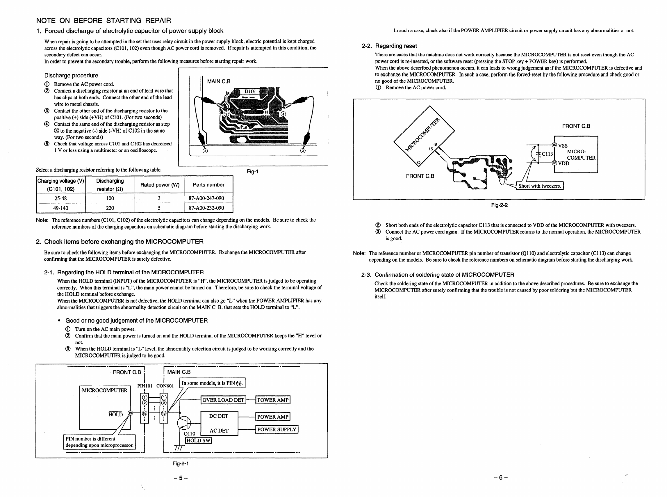
1. Forced discharge of electrolytic capacitor of power supply block
When repair is going to be attempted in the set that uses relay circuit in the power supply block, electric potential is kept charged
across the electrolytic capacitors (C101, 102) even though AC power cord is removed. If repair is attempted in this condition, the
secondary defect can occur.
In order to prevent the secondary trouble, perform the following measures before starting repair work.
Discharge procedure I II
--
Remove the AC Dowercord, I I II MAIN C.B
Connect adisch;ging resistor at an end of lead wire that
has clips at both ends. Connect the other end of the lead
wire to metal chassis,
Contact the other end of the discharging resistor to the
positive (+) side (+VH) of C101. (For two seconds)
Contact the same end of the discharging resistor as step
@to the negative (-) side (-VH) of C102 in the same
way. (For two seconds)
Check that voltage across C1OI and C102 has decreased
1Vor less using amultimeter or an oscilloscope. 66
I
Select adischarging resistor referring to the following table. Fia-1
ICharging voltage (V) Discharging Rated power (W) Parts number
(Clol, 102) resistor (Q) I
I25-48 I100 13 I87-AOO-247-090 I
I49-140 I220 15 I87-AOO-232-090 I
Note: The reference numbers (C101, C102) of the electrolytic capacitors can change depending on the models. Be sure to check the
reference numbers of the charging capacitors on schematic diagram before starting the discharging work.
2. Check items before exchanging the MICROCOMPUTER
Be sure to check the following items before exchanging the MICROCOMPUTER. Exchange the MICROCOMPUTER after
confirming that the MICROCOMPUTER is surely defective.
2-1. Regarding the HOLD terminal of the MICROCOMPUTER
When the HOLD terminal (INPUT) of the MICROCOMPUTER is “H”, the MICROCOMPUTER is judged to be operating
correctly. When this terminal is “L”, the main power cannot be turned on, Therefore, be sure to check the terminal voltage of
the HOLD terminal before exchange.
When the MICROCOMPUTER is not defective, the HOLD terminal can also go “L” when the POWER AMPLIFIER has any
abnormalities that triggers the abnormality detection circuit on the MAIN C. B. that sets the HOLD terminal to “L”.
●Good or no good judgement of the MICROCOMPUTER
@Turnon the AC main power,
@Confirm that the main power is turned on and the HOLD terminal of the MICROCOMPUTER keeps the “H” level or
not.
~When the HOLD terminal is “L” level, the abnormality detection circuit is judged to be working correctly and the
MICROCOMPUTER is judged to be good.
I—.— .—. ——.— .—. —.—. —.—
I
FRONT C.B :IMAIN C.B
e
111I
l.;)!~
I
PIN101 CON601
MICROCOMPUTER Il?Rlwf+ OVER LOAD DET POWER AMP
A-J (’%
=D 19— b-6
. . . DC DET
.●.POWER AMP
..
I‘%10 I‘CDETIIPOWER SUPPLY I
PIN number is different
depending upon microprocessor.
—.— .—. —.]L771-
.—. —.— .— .— .—-.
In such acase, check also if the POWER AMPLIFIER circuit or power supply circuit has any abnormalities or not.
2-2. Regarding reset
There are cases that the machine does not work correctly because the MICROCOMPUTER is not reset even though the AC
power cord is re-inserted, or the software reset (pressing the STOP key +POWER key) is performed.
When the above described phenomenon occurs, it can’leads to wrong judgement as if the MICROCOMPUTER is defective and
to exchange the MICROCOMPUTER. In such acase, perform the forced-reset by the following procedure and check good or
no good of the MICROCOMPUTER.
@Remove the AC power cord.
Fig-2-2
@Short both ends of the electrolytic capacitor Cl 13 that is connected to VDD of the MICROCOMPUTER with tweezers.
@Connmt the AC power’ cord a@n. If theMICROCOMPUTER returns to the normal operation, the MICROCOMPUTER
is good.
Note: The reference number or MICROCOMPUTER pin number of transistor (Ql 10) and electrolytic capacitor (Cl 13) can change
depending on the models. Be sure to check the reference numbers on schematic diagram before starting the discharging work.
2-3. Confirmation of soldering state of MICROCOMPUTER
Check the soldering state of the MICROCOMPUTER in addition to the above described procedures. Be sure to exchange the
MICROCOMPUTER after surely confirming that the trouble is not caused by poor soldering but the MICROCOMPUTER
itself.
Fig-2-1
-5- -6-
jomi
ELECTRICAL MAIN PARTS LIST
I If can’t understand for Description please kindly refer to” REFERENCE NAME LIST”. I
REF.NO. PARTNO. IaNfll DESCRIPTION
No.
IC
87-A2O-O83-O1O
88-MA4-61O-O1O
87-NF8-614-O1O
87-017-889-010
87-017-888-080
87-017-915-080
87-A2O-715-O1O
87-A20-613-040
87-070-127-110
87-A2O-438-O1O
87-A2O-913-O1O
TRANSISTOR
89-213-702-010
89-333-317-880
87-A30-198-080
87-A30-196-080
89-113-187-880
87-A30-197-080
87-026-219-080
87-A30-087-080
87-A30-074-080
87-A30-084-080
87-A30-073-080
87-026-239-080
87-A30-190-080
87-A3O-1O9-O1O
87-A3O-1O8-O1O
87-A30-091-080
87-A30-090-080
87-026-218-080
87-026-214-080
87-A3O-137-O1O
87-A3O-138-O1O
DIODE
87-070-274-080
87-070-178-090
87-A40-435-080
87-A40-470-080
87-A40-345-080
87-002-225-010
87-017-931-080
87-A40-466-080
87-A40-234-080
87-A40-004-080
MAIN C.B
Clol
Clol
C102
C103
C104
C105
C106
C107
C108
C109
Cllo
Clll
C112
C113
C114
C122
C123
87-016-495-090
87-010-917-090
87-010-385-080
87-010-917-090
87-A1O-627-O9O
87-018-127-080
87-010-408-080
87-010-384-080
87-010-381-080
87-010-384-080
87-010-384-080
87-010-247-080
87-010-263-080
87-010-404-040
87-010-374-080
87-010-384-080
87-010-384-080
IC,BA3835S
IC,UPD780228-XXX-XXX
IC,SPS-442-1-W
IC,NJM4558LD
IC,NJM4558MDcHE>
C-IC,BU4094BCF<LH>
IC,M62439SPcLH>
C-IC,BU9262AFS<LH>
IC,LC72131D
IC,LA1837CEXCEPT HE>
IC,LA1837NLCHE>
TR,2SB1370
TR,2SC3331
TR,KTC3199GR
TR,2SC4115SRS
TR,2SA1318
TR,KTA1267GR
TR,DTA144ES
C-FET,2SK2158
C-TR,RTIP 141C
C-TR,CSB1058B
C-TR,RTIN 141C
C-TR,DTC114TK<LH ONLY>
TR,CC5551
TR,2SD2495<555U,HE>
TR,2SB1626<555U,HE>
FET,2SJ460
FET,2SK2541
TR,DTC144ES
TR,DTA114YS
TR,2SD2494<LH,554U>
TR,2SB1625<LH,554U>
DIODE,1N4003 SEM
DIODE, 1N5402-BD54<555U>
ZENER,MTZJ30D
DIODE,1SS254
ZENER,MTZJ1OC
DIODE,DBF4OC-K1O<EXCEPT555U>
ZENER,MTZJ5.6B
ZENER,MTZJ2.7A
ZENER,MTZJ5.6A
ZENER,MTZJ16A<555U>
CAP,E 3300-25 SMG<EXCEPT555U>
CAP,E 3300-50 MSMG<555U>
CAP, ELECT 220-25V<EXCEPT 555U>
CAP,E 3300-50 MSMG<EXCEPT555U>
CAP,E 2200-50 MSMG
CAP, CER 470P-50V
CAP, ELECT 47-50V
CAP, ELECT 1OO-25V
CAP, ELECT 330-16V
CAP, ELECT 1OO-25V
CAP, ELECT 1OO-25V
CAP, ELECT 1OO-5OV
CAP, ELECT 100-1OV
CAP, E4,7-50 HSME
CAP, ELECT 47-1OV
CAP, ELECT 1OO-25V
CAP, ELECT 1OO-25V
REF,NO. PARTNO. IWNRI DESCRIPTION
No.
C124
C130
C207
C208
C209
C21O
C211
C212
C213
C214
C219
C220
C229
C230
C235
C236
C237
C301
C302
C303
C304
C307
C308
C315
C317
C318
C360
C361
C401
C402
C403
C404
C411
C412
C452
C458
C459
C461
C462
C601
C602
C611
C612
C613
C614
C615
C616
C617
C701
C702
C703
C704
C705
C706
C707
C709
C71O
C712
C713
C714
C715
C746
C753
C756
C757
C758
C759
C761
C762
C763
87-018-134-080
87-018-131-080
87-010-546-080
87-010-546-080
87-018-133-080
87-018-133-080
87-010-404-080
87-010-404-080
87-010-260-080
87-010-260-080
87-010-544-080
87-010-544-080
87-018-123-080
87-018-123-080
87-018-209-080
87-018-209-080
87-018-134-080
87-018-195-080
87-018-195-080
87-018-195-080
87-018-195-080
87-010-263-080
87-010-263-080
87-010-374-080
87-010-546-080
87-010-546-080
87-010-401-080
87-010-374-080
87-010-401-080
87-010-401-080
87-018-128-080
87-018-128-080
87-010-405-080
87-010-405-080
87-010-382-080
87-018-131-080
87-018-128-080
87-018-126-080
87-018-126-080
87-018-195-080
87-018-195-080
87-010-545-080
87-010-545-080
87-010-545-080
87-010-545-080
87-018-104-080
87-010-408-080
87-010-408-080
87-010-404-080
87-018-134-080
87-018-134-080
87-018-131-080
87-018-131-080
87-018-131-080
87-010-112-080
87-010-248-080
87-010-112-080
87-018-149-080
87-018-149-080
87-010-112-080
87-018-119-080
87-018-134-080
87-010-408-080
87-018-134-080
87-018-134-080
87-010-112-080
87-018-134-080
87-010-404-080
87-010-400-080
87-010-401-080
CAPACITOR,TC-U 0.01-16
CAP,CER 1OOOP-5OV
CAP, ELECT 0.33-50V
CAP, ELECT 0.33-50V
CAPACITOR,CER 4700P-16V
CAP,
CAP ,
CAP,
CAP ,
CAP,
CAP,
CAP ,
CAP,
CAP,
CAP ,
CAP,
CAP,
CAP,
CAP,
CAP,
CAP ,
CAP,
CAP ,
CAP,
CAP *
CAP,
CAP,
CAP,
CAP,
ELECT 4.7-50V
ELECT 4.7-50V
ELECT 47-25V
ELECT 47-25V
ELECT 0.1-50V
ELECT 0.1-50V
TC-U 220P-50 KB
TC-U 220P-50 KB
CER 0.1-50V
CER 0.1-50V
TC-U 0.01-16 YN
TC-U 1200P-16 M
TC-U 1200P-16 M
TC-U 1200P-16 M
TC-U 1200P-16 M
ELECT 100-1OV
hLECT loo-lov
ELECT 47-1OV
ELECT 0.33-50V
ELECT 0.33-50V
ELECT 1-50V
ELECT 47-1OV
ELECT 1-50V
ELECT 1-50V
CAP,TC-U 560P-50 KB
CAP,TC-U 560P-50 KB
CAP, ELECT 1O-5OV
CAP, ELECT 1O-5OV
CAP, ELECT 22-25V
CAP, CER 1OOOP-5OV
CAP, CERA-SOL SS 560P
CAP,TC-U 390P-50 B
CAP,TC-U 390P-50 B
CAP, CER 1200P-16V
CAP, CER 1200P-16V
CAP, ELECT 0.22-50V
CAP, ELECT 0.22-50V
CAP, ELECT 0.22-50V
CAP, ELECT 0.22-50V
CAP,TC-U 1OP-5O SL
CAP, ELECT 47-50V
CAP, ELECT 47-50V
CAP, ELECT 4.7-50V
CAPACITOR,TC-U 0.01-16
CAP, CER 1OOOP-5OV
CAP, CER 1OOOP-5OV
CAP, CER 1OOOP-5OV
CAP, ELECT 100-16V
CAP, ELECT 22O-1OV
CAP, ELECT 100-16V
CAP,TC-U 15P-50 CH
CAP,TC-U 15P-50 CH
CAP, ELECT 100-16V
CAP, TC-U 1OOP-5O KB
CAPACITOR,TC-U 0001-16
CAP, ELECT 47-50V
CAPACITOR,TC-U 0001-16
CAPACITOR,TC-U 0.01-16
CAP, ELECT 100-16V
CAPACITOR,TC-U 0.01-16
CAP, ELECT 4.7-50V
CAP, ELECT 0.47-50V
CAP, ELECT 1-50V
REF.NO,PARTNO. KMJRI DESCRIPTION
C764
C765
C766
C768
C769
C770
C771
C773
C774
C783
C784
C785
C786
C787
C787
C788
C788
C789
C790
C803
C804
C808
C813
CF801
CON351
FC101
FFE801
J203
J601
J801
L201
L202
L451
L701
L771
L772
L801
L981
R124
R126
R223
R224
R249
R250
R723
RYOO1
SFR451
SFR452
Wlol
X701
FRONT C.B
C150
C151
C152
C153
C154
C201
C203
C204
C205
C206
C207
C208
C209
C21O
C211
C212
C214
87-010-196-080
87-010-196-080
87-010-196-080
87-010-196-080
87-010-196-080
87-018-209-080
87-010-198-080
87-018-127-080
87-010-316-080
87-010-318-080
87-010-312-080
87-010-196-080
87-010-494-040
87-010-248-040
87-010-194-080
87-010-263-040
87-010-405-040
NO.
87-010-401-080
87-018-115-080
87-010-407-080
87-018-208-080
87-010-403-080
87-018-134-080
87-010-406-080
87-018-131-080
87-010-405-080
87-018-199-080
87-018-199-080
87-010-405-080
87-010-405-080
87-018-196-080
87-018-132-080
87-018-196-080
87-018-132-080
87-010-403-080
87-010-403-080
87-018-134-080
87-018-134-080
87-018-134-080
87-018-131-080
87-008-261-010
86-NF7-64O-O1O
88-906-251-110
A8-8ZA-190-030
87-A6O-398-O1O
87-A6O-398-O1O
87-A6O-2O2-O1O
87-003-383-010
87-003-383-010
87-007-342-010
87-005-847-080
87-A5O-266-O1O
87-A9O-733-O1O
87-005-847-080
87-NF4-65O-O1O
87-AOO-320-080
87-022-200-080
87-AOO-258-080
87-AOO-258-080
87-AOO-258-080
87-AOO-258-080
87-AOO-320-080
87-A9O-464-O1O
87-A90-432-080
87-A90-432-080
85-NF5-628-O1O
87-A7O-O61-O1O
CAP, ELECT 1-50V
CAP, CER 47P-50V
CAP, ELECT 33-50V
CAP 0.047-50F
CAP, ELECT 3.3-50V
CAPACITOR,TC-U 0.01-16
CAP, ELECT 22-50
CAP, CER 1OOOP-5OV
CAP, ELECT 1O-5OV
CAP, CER 3300P
CAP, CER 3300P
CAP, ELECT 1O-5OV
CAP, ELECT 1O-5OV
CAP, CER 1500P-16V<HE>
CAP, CER 2200P-16V<LH,U>
CAP, CER 1500P-16V<HE>
CAP, CER 2200P-16V<LH,U>
CAP, ELECT 3.3-50V
CAP, ELECT 3.3-50V
CAPACITOR,TC-U 0001-16
CAPACITOR,TC-U 0.01-16
CAP, CER 1OOOP-5OV
FILTER, SFE1O.7MA5-A
CONNASSY,8P-RPB
FF-CABLE,6P 1.25
8ZA-1 FEUNM
JACK PIN 2P R/W<EXCEPT 555U>
JACK,PIN 2P R/W HSP-242V24
TERNINAL,ANT 4P MSP-154V-02
COIL,lUH-S
COIL,lUH-S
COIL,OSC 85K BIAS
COIL,202UH(CECS)
COIL,FM DET-2N(TOK)
FLTR,PCFAZH-450 (TOK)
COIL,2.2UH(CECS)
COIL,AM PACK 4N(TOK)
RES,M/F 3.3-l/4W FSN2E<U>
RES,M/F 0.56-lWJ
RES,M/F 0.22-lWJ
RES,M/F 0.22-lWJ
RES,M/F 0.22-lWJ
RES,M/F 0.22-lWJ
RES,M/F 3.3-l/4W FSN2E<U>
RELAY, DG12D2-O(M)CEXCEPT 555U>
SFR,30K HNVZ6TLTA
SFR,30K HNVZ6TLTA
F-CABLE 7P-2.5<EXCEPT 555U>
VIB,XTAL 4.500MHZ CSA-309
CHIP CAPACITOR,O.1-25
CAP, CER 0.1-50V<LH,HE>
CAP, CHIP 0,022
CAP, CER 470P-50V
C-CAP,S 33P-50 CH
C-CAP,S 47P-50 CH
C-CAP,S 15P-50 CH
CHIP CAPACITOR,O.1-25
CAP,E 1-50 GAS
CAP,E 220-10 SME
CAP, CHIP 0.047
CAP,E 100-10
CAP,E 10-50
REF,NO. PARTNO. WNRI DESCRIPTION
NO,
C301
C354
C355
C401
C402
C404
C405
C406
C501
C502
C504
C505
C506
C508
C509
C601
C602
C609
C61O
C611
C612
C613
C614
C615
C616
C617
C618
C701
C702
C703
C704
C705
C706
C707
C708
C709
C71O
C712
C713
C714
C715
C716
C718
C719
C725
C936
C937
C938
C939
C940
C941
C942
C943
C944
C945
C946
C947
C948
CON501
FC102
FL401
L701
LED209
LED21O
LED211
LED212
LED218
LED219
LED220
S401
87-010-384-040
87-010-196-080
87-010-196-080
87-010-406-040
87-010-406-040
87-010-194-080
87-010-246-040
87-018-134-080
87-010-401-040
87-010-177-080
87-010-544-040
87-010-321-080
87-010-401-040
87-010-248-040
87-010-545-040
87-010-404-040
87-010-404-040
87-010-213-080
87-010-213-080
87-010-545-040
87-010-545-040
87-010-545-040
87-010-545-040
87-010-154-080
87-010-408-040
87-010-408-040
87-010-408-040
87-010-319-080
87-010-319-080
87-012-141-080
87-010-197-080
87-010-180-080
87-010-213-080
87-010-213-080
87-010-197-080
87-010-181-080
87-010-196-080
87-010-234-040
87-010-071-040
87-010-071-040
87-010-183-080
87-010-183-080
87-010-196-080
87-010-263-040
87-012-141-080
87-012-140-080
87-012-140-080
87-012-140-080
87-012-140-080
87-012-140-080
87-012-140-080
87-012-140-080
87-012-140-080
87-012-140-080
87-012-140-080
87-012-140-080
87-012-140-080
87-012-140-080
86-NFZ-635-O1O
88-914-231-110
88-MA4-601-O1O
87-005-448-080
87-070-201-080
87-070-201-080
87-070-201-080
87-070-201-080
87-070-201-080
87-070-201-080
87-070-201-080
87-A90-095-080
CAP,E 100-25 SME
CHIP CAPACITOR,O.1-25
CAP,E 22-50 MSME
CAP,E 22-50 MSME
CAP, CHIP 0.047
CAP,E 47-35 SHE
CAPACITOR,TC-U 0.01-16
CAP,E 1-50 SME<HE>
C-CAP,S 820P-50 SL<HE>
CAP,E 001-50 SME<HE>
CHIP CAPACITOR,82P(J)<HE>
CAP,E 1-50<HE>
CAP,E 220-10 SME<HE>
CAP,E 0.22-50 SME<HE>
CAP,E 407-50 SME<LH>
CAP,E 4.7-50 SME<LH>
C-CAP,S 00015-50 B<LH>
c-~,S 00015-50 B<LH>
CAP,E 0.22-50 SME<LH>
CAP CHIP 10P<LH>
CAP,E 47-50 SME<LH>
CAP,E 47-50 SME<LH>
CAP,E 47-50 SMEXLH>
C-CAP,S 56P-50 CH<LH>
C-CAP,S 56P-SO CHCLH>
CHIP-CAPACITOR, 0.22-16FcLH>
CAP, CHIP 0.01 DMcLIi>
C-CER 1500P<LH>
C-CAP,S 0.015-50 B<LH>
CAP, CHIP 0.01 DM<LH>
CAP,CHIP S1800P<LH>
CHIP CAPACITOR,O.1-25<LH>
CAP,E 47-16 5L<LH>
CAP,E 1-50 5L<LH>
CAP,E 1-50 5L<LH>
C-CAP,S 2700P-50 B<LH>
CHIP CAPACITOR,O.1-25<LH>
CAP,E 1OO-10<LH>
CHIP-CAPACITOR, 0.22-16F<LH>
C-CAP,S 470P-50 JC?i
C-CAP,S 470P-50 JCH
C-CAP,S 470P-50 JCH
C-CAP,S 470P-50 JCH
C-CAP,S 470P-50 JCH
C-CAP,S 470P-50 JCH
C-CAP,S 470P-50 JCH
C-CAP,S 470P-50 JCH
C-CAP,S 470P-50 JCH
C-CAP,S 470P-50 J.CH
C-CAP,S 470P-50 JCH
C-CAP,S 470P-50 JCH
C-CAP,S 470P-50 JCH
CONNASSY,9P MECHA
FF-CABLE,14P 1.25
FL,BJ611GK
COIL 220UH,KdH>
LED,SLP9118C-51-S-T1
LED,SLP9118C-51-S-T1<LH>
SW,TACT EVQ11G04M
-J –8–
jomi
TRANSISTOR ILLUSTRATION
REF.NO, PARTNO. KANRI DESCRIPTION REF.NO. PARTNO. KANRI DESCRIPTION
NO. NO,
S402
S403
S404
S405
S406
S407
S408
S409
S41O
S411
S412
S413
S414
S415
S416
S417
S418
S419
S420
S421
S422
S423
S424
S426
S427
S428
SFR301
SW201
SW202
VR501
X201
87-A90-095-080
87-A90-095-080
87-A90-095-080
87-A90-095-080
87-A90-095-080
87-A90-095-080
87-A90-095-080
87-A90-095-080
87-A90-095-080
87-A90-095-080
87-A90-095-080
87-A90-095-080
87-A90-095-080
87-A90-095-080
87-A90-095-080
87-A90-095-080
87-A90-095-080
87-A90-095-080
87-A90-095-080
87-A90-095-080
87-A90-095-080
87-A90-095-080
87-A90-095-080
87-A90-095-080
87-A90-095-080
87-A90-095-080
87-024-169-080
87-A9O-535-O1O
87-A9O-792-O1O
88-MA4-609-O1O
87-A70-075-080
SW,TACT EVQ11G04M
SW,TACT EVQ11G04M
SW,TACT EVQ11G04M
SW,TACT EVQ11G04M
SW,TACT EVQ11G04M
SW,TACT EVQ11G04M
SW,TACT EVQ11G04M
SW,TACT EVQ11G04M
SW,TACT EVQ11G04M
SW,TACT EVQ11G04M
SW,TACT EVQ11G04M
SW,TACT EVQ11G04M
SW,TACT EVQ11G04M
SW,TACT EVQ11G04M
SW,TACT EVQ11G04M
SW,TACT EVQ11G04M
SW,TACT EVQ11G04M
SW,TACT EVQ11G04M<LH>
SW,TACT EVQ11G04M
SW,TACT EVQ11G04M<LH>
SW,TACT EVQ11G04M
SW,TACT EVQ11G04M<LH>
SW,TACT EVQ11G04M
SW,TACT EVQ11G04M
SW,TACT EVQ11G04M
SW,TACT EVQ11G04M
SEMI-FIXED RESISTOR, 2.2K
SW,RTRY EC16B24304
SW,RTRY EC12E12244 ENCORDER
VR,SL 10KB RS15111<HE>
VIB,CER 4.19MHZ CRHF
AC1 C.B
~F101
i
!F101
!F101
!F101
!FC1
i
!FC2
!FC101
!FC102
IPT101
~PT101
~PT101
8
!PT101
!Swlol
!T1
IT2
AC2 C.B
k!FO04
FO05
A
!PRO04
!PRO05
ROO1
RO02
~ROO1
~RO02
SUB C*B
CNA101
87-035-402-010
87-035-190-010
87-035-415-010
87-035-366-010
87-A90-505-080
87-A90-505-080
87-033-147-010
87-033-147-010
88-MA4-616-O1O
88-MA4-617-O1O
88-MA4-618-O1O
88-MA4-619-O1O
87-A9O-165-O1O
87-A6O-317-O1O
87-A6O-317-O1O
FUSE,2A 250V F235<555U>
FUSE,2A 250V T218<HE>
FUSE,2.5A 250V T239UL<554U>
FUSE,2.5A 250V T<LH>
FUSE CLAMP,TPO0351-51<U>
FUSE CLAMP,MT<LH,HE>
FUSE CLAMP,NT<LH,HE>
PT,LH<LH>
PT,UAC554U>
PT,BE<HE>
PT,U<555U>
SW,SL 1-2-3 SWS2301<LH,HE>
TERMINAL, 1P MSC<U>
TERMINAL, 1P MSC<U>
ECB ECB BCE ECB
2SC3331
2SA1318 CC5551
CSB1058 2SB1625
2SB1626
2SB1370
2SD2494
2SD2495
DTC144ES
DTA114YS
DTA144ES
P
0
87-026-690-080
87-026-690-080
87-026-681-080
87-026-681-080
87-AOO-261-080
87-AOO-261-080
87-026-681-080
87-026-681-080
FUSE,5A 125V 251<U>
FUSE,5A 125V 251<U>
PROTECTOR,5A 60V 491cLH,HE>
PROTECTOR,5A 60V 491<LH,HE>
RES,M/F O.56-lW J<U>
RES,M/F 0.56-lW ~<U>
PROTECTOR,5A 60V 491<LH,HE>
PRoTEcToR,5A 6ov 491<LH,HE>
BCE SDG SDG
2SK2541KTA1267
KTC3199 2SC4115S 2SJ460
86-2G1-664-O1O CONN,ASSY 5P SUB2
MIC C.B<HE>
J501 87-099-659-010
RY C.B<LH>
RY201 87-A9O-713-O1O
JACK,6.3 JY-6314-01130
RELAY,12V DQ12D1-OS(M)
DTC114TK
RT1N141C
RT1P141C
2SK2158
05-Y7#wmwla~– F/CHIPRESISTOR PARTCODE
+’Y7%HN$IL%Z-- Fah!i!)zz%l
Chip Resistor Part Coding
EIml-nctn ❑lclcl
Resistor Code L~Jfi@
Value of resistor
+7mm
Chip resistor
T
%ft MM B%i%’%i m%’ ~&/Dimensions (mm) ~lk~fi~-b’ :A
Wattage Type Tolerance Symbol fi%/Form f- WtResistor Code: A
l/16W 1608 *5%
I/low 2125 *5%
l/8W 3216 *5% :- -’ ‘: : : :
–9– –lo–
jomi
BLOCK DIAGRAM -1 (MAIN/ FRONT)
TO CO HECHAN15H ,—. —.— -—-— -—. —-— -—- —- 1
bZt3- I
/ \ ❑tAAINc.B
1P PO]NT
-r—-— -—- CON35I
,. BIAS 09C
WS31 454
L4S1 )
Wc
f- 1
I
wlc401
2443 NJN45S8L0
!EC REC EC’ a
!UTE AHP -
RPli --,, ;
l._~ II I
L
~
....- -“* 0303! 304
mre I==),.
I
II
I
I
I
I
I
1
I
I
I
I
I
I
I
I
I
I
I
I.,
IIo
,
,
I
l!
II
11
CO-L
A-QND
CO-R
CEI ON
EI-ofw
Wi
I1LI4I
Im[1 “a-
“.”. “. . .
OECK1Wmll IIG’ a, G”G”
PLL CE j
F=
9ATA
CLK
~/l FC
TH BA9E
7UN-L
TUN-R
TU-ON
bEc,, ~
o
VREF II ICifol
NJN455BM H
‘r 1
0301, 302
OECK2
PB w
$
N(.J :$z
z z
.
PH LCH
RCH —
I
1.%01 I1,I
-A
ml ..l ,-”. ”, II 1.— Il”,d:!!,ly,F?l ‘uX-L+ L-CH
lrf. nl
P-ml
TIII I*’. v
,II
I1~ I I I I I
a0201 ‘e
R
OIOOE 5
0207, y
9238 u
OIFFERENTIAL
AtiP VOLTAOE CW;NT
0201, 203
02013207 :2~9 0211.213
I
CONIOIh
1
2
x
J201
)202
1,.- It%- 1- ‘-’ w“ II-LX 14 +1
CONIROL ,, fJATk
*
0204 v
TN-BASE BUFFER
~
11II
DIFFERENTIAL VOLTA03
ANP CURRENT I
0202204
020& 208 1)2% 021T214
.L
Vo
I
:LE9210
:/
fLE0220 Nm
,
~
8100E
a220% 222 RE~ pLAY~.
PLAYI
d
HOTOR
MOTOR9RI W
0303 +.“. If!4 II
I. .. 1
po& 218}—————— ~I
m1-VP 1J
riiii---” ---- --”””-f ‘-----1 EXCEPT5S5U
ir~l !r -—-— I...........----------------.....
-1
+
B=Tam
I
I11:1 11111 1111 IL-,. .I-— t
,RYOOI ,
,
9111%1121 Ill *-- ‘Lwc’ C“”il ~
Ill
ILH ONLY !I
020S, 206
.......................................... [-1
J-1 t-! IJelo5*lo9 I j 1............. .. ... ........I
r$%l-- -Jv2nl II I I“l-t%,,,
(IA)“1
I
“AC ~20V :
60HZ;
N19 !
U20
d!u .
\
I’./q-’l ,UJ
................................
I
iia Sal--.--d. g1Ill 1Al+ II
1
~-.w —
Y>
YJ_Y!___!!__L:_- /I
_- —_ —-_i i—-— l----””------”--------------w-ii-tii
~i~l
I1
................................................................................................................
IC701
EU%!62AFS
AQ1
m- Wvl 1I
I
AC1 I
!C.BI
I
,
0
,
,AC120V/
AC;~;vti
!1
L...............................
,.3
==
-la i
I. . e.?
I230V/
..........
~Icbol
H624399P
LH ONLY I
I.........................................................................................................................I
I
I❑FRONT C.B
I
-11- -12-
jomi
BLOCK DIAGRAM -2 (TUNER)
r-—-—- BLOCK)
I
I
I
I
I
I
I
I
I
(TUNER L772
.AMIFT .
-tCF
AMIF AMIF +
OUT IN
IAM IF
$
J801 LA183’7
~
IC75
mmml
L981 AM PACK
[MW TRACKING ABJIMW ANT
rl “—— —~l— ——— ——— ——— ——— ———1 /3
2
3
q‘“ ~qa ]7
L————— .———— ———.— ——.——
14 6
AM RF
AM Osc REG
1
)
~S-CURVE~ MAIMX
7
)+ AM RF
AMP
--l AGC II
iQ
STEREO
Sw
II
‘R-O
\AMIFO/=
%
PILOT
9ET
7
II
I
IFMIF
d)-+ )
o
m
-1
E
u-)
>
w
z
2
L
.
CF80 4
OSCOUT
FFE801 8ZA-1 FEUNM
IFM FRONT ENi31 7
Vcc <
ANT
GN9
ITI
(J
17
.
STEREO
GNO +13 VT A+13
FM
BANO SW (
Q801
FOSC /
IF-IN IF-MUTE AMIN MONO
/3EAT
e
TPI
(VT)
)i=msw
I
IC701
LC72131
n
PLL
)FM-IN
AOUT AIN PQ XIN XOUT I
VT 1+ 141P
X701
4* 5MHZ
- - -—
-13- -14-
jomi
TO CO ME
~––––_
I
I
I[
s
s
15PEAKER
L––– –-.
EIEcK21
i%
YY+
Z-lr
am>
CON301 [3 1]
&
–-i5–– –-l&––
,.,.
jomi