Akai LTA-26C904 User manual

SERVICE MANUAL
Model:
LTA-26C904
LTA-32C904
www.akai.ru
LCD TV

1
Catalog
Chapter1 Characteristic of LSO1 core and the constitution of the
whole machine..............................................................................................................................2
Chapter2 Function introduction of ICs or functional module of
Akai LCD TV with LS01core...............................................................................................7
Chapter3 Whole Machine Signal Processing Analysis and
Measured Data at the Key Points................................................................................27
Chapter4 Familiar Problem and Processing..................................................37
Chapter5 Listing of Repair and Easily Damaged Parts........................38
Chapter6 Factory Mode Setting and Notes.....................................................39
Appendix: 1. Schematic diagram of LCD TV with LS01 core
2. Schematic diagram of power module
3. Assembly diagram of LCD TV with LS01 core
4. Wiring diagram of LCD TV with LS01 core

2
Chapter 1 Characteristic of LSO1 core and the constitution of the
whole machine
1. Models embedding LS01 core:
Region Other regions
Original
machine
LTA-26C904
LTA-32С904
2. Main specifications of TV
Region Other regions
Color
mode PAL、NTSC、SECAM
RF signal Sound
mode
PAL-D/K、B/G、I
SECAM-D/K、B/G
NTSC-M
Video(or Y/C)signal PAL,NTSC,NTSC4.43,
SECAM
Program presetting 236 sets(0-235)
Sound Power (THD
≤7%)5W+5W
Power voltage 100V~240V
Graphics and text 100 pages
VCHIP、CCD X
Sound NICAM、IGR
SCART interface X
VGA signal input Yes
YpbPr HD signal input Yes
HDMI digital signal
input Yes
Earphone Yes
OSD language English, French, German, Russian
Automatic shut down if
no signal Automatically enter into standby state after 5 minutes in TV no signal state
Program reserve
function
Capable of reserving 5 sets program jumping time, if time is up to the reserved time,
automatically jump to the corresponding program
Channel exchange
and sorting Customer could rearrange the channels according to personal habit
Energy saving function Customer could adjust LCD screen backlight brightness manually. Appropriately
reducing the backlight brightness could save energy.
Plug and Play LCD TV could be used as computer screen, no need for the installation of software,
which is Plug and Play in real sense
3. Circuit constitution of the whole machine
Akai LCD TV with LS01 core is made up of switch power, system control circuit, video
processing circuit, audio processing circuit, sound power amplifier circuit, AV input circuit,
LCD screen module. Block circuit diagram of the whole machine is shown as below:
1) European market:

3
2). American and Asian market:

4

5
4. Introduction of printed board module
Akai LCD TV with LS01 is made up of power board, side AV board, remote control
reception board, key board, and mainboard. The table below is the introduction of the function
of all printed board modules.
No. Designation o
f
module Function description
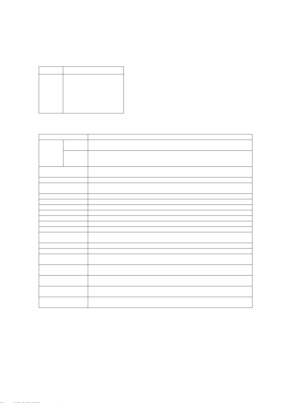
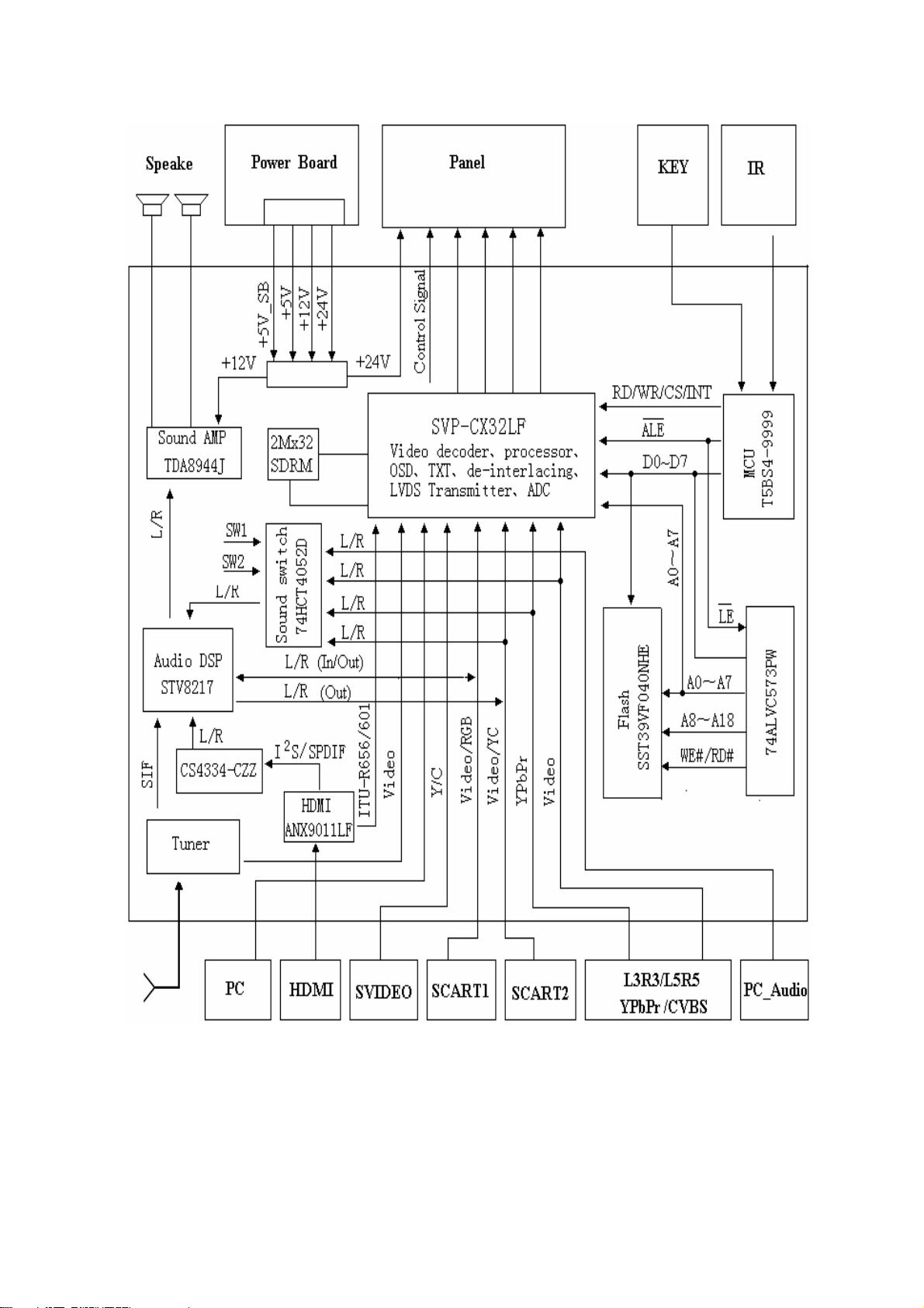
1 Mainboard
module
Mainboard module is the core part of LCD TV signal processing. Unde
r
the control of the system control circuit, It undertakes the task o
f
converting the external input signal into the unified digital signal that the
LCD screen could identify. Mainboard controls the whole machine
through MCU bus, decode VIDEO signal, controls the image analog
quantity (brightness, contrast, chroma, hue, definition etc), adjusts white
balance, generates OSD, de-interlaces signal, converts signal frequency,
and finishes signal A/D and D/A conversion, video enhancement, LVDS
signal coding and output; it has Scart interface, “S” terminal, AV terminal,
Ypbpr, HDMI and PC interface, Tuner input, sound demodulation, sound
effect treatment, sound power amplifier, and online upgrade of program.
2
Remote
reception board
module
The remote reception board module is constituted by an indicator-light
and a remote reception-head. Customer could manipulate the LCD TV by
using remote controller very conveniently. By the color of the indicato
r
light, the operation mode of the LCD TV could be judged (red is standby,
green is power on).
3 Built-in powe
r
board module
Convert the 100V~240V AC into DC, output have +24v, +12V, +5V, and
the +5V_stb in standby state.
4 Keyboard
module
Keyboard module has 7 function keys (program increase/decrease,
volume increase/decrease, AV/TV switch, menu key, on/standby control),
customer could use the key of the machine to manipulate the LCD TV.
5 LCD screen
module
LCD screen has built-in inverter that convert DC into high voltage AC
signal to ignite the backlight CCFL (Cold Cathode Fluorescent Light); the
LCD screen process the video signal from signal board and reappear.
6 Side AV board Side AV board is used for earphone output.

6
Chapter 2 Function brief introduction of main ICs of
LCD TV with LS01 core
1. Main ICs and functional modules of Akai LCD TV with LS01core
No. Item no. Model Main function
1 U15 JS-6H2/121 High frequency head, output sound and image
video signal
2 U1 SVP-CX32LF Video decode, image processor, A/D and D/A
conversion
3 U2 IS42S32200C1-6TL SDRAM with 2MX32bits, used for the access of
image signal.
4 U3 AT24C64A-10PU-2.7 EEPROM
5 U4 T5BS4-9999 MCU,main control IC
6 U5 SST39VF040-70-4C-NHE Flash, whole machine control program is in it
7 U6 74ALVC573PW Address latch, to latch the address wires
8 U8 TCM809SENB713 Hardware reset IC of MCU
9 U9 74HCT4052D Audio input switch of AV terminal
10 U35 STV-8217/STV-8218 Audio signal processor
11 U14 74LVC14AD VGA line and field synchronizing signal waveform
shaping
12 U16、U25 AT24C02BN-10SU-1.8 EEPROM
14 U18、U22 AZ1117H -1.8TRE1 3.3V to 1.8V DC level conversion
16 U19、U24 AZ1117H -3.3TRE1 5V to 3.3V DC level conversion
18 U20 AZ1084S -3.3TRE1 5V to 3.3V DC level conversion
19 U21 AZ1084S -1.8TRE1 5V to 1.8V DC level conversion
20 U23 AZ78L08ZTR-E1 12V to 8V DC level conversion
21 U26 CS4344-CZZ HDMI digital audio decode, D/A conversion
22 U28、U29 Rclamp0514M.TBT ESD protection device of HDMI input terminal
24 U30 ANX9011L HDMI digital signal decode
25 U31 PI5C3306LE Bus (SDA, SCL) switch used for program update
26 U33 TDA8944J Sound power amplifier (BTL output)

7
2. Function introduction of ICs or functional module of Akai LCD TV with LS01core
1.Hign frequency head(JS-6H2/121)
Pin No. Definition of pin Function description
1 NC No connection
2 BT No connection
3 VCC +5V power
4 SCL IIC bus (clock)
5 SDA IIC bus (data)
6 AS Ground
7 AFS Ground
8 NC No connection
9 NC No connection
10 NC No connection
11 SIF/Out AGC control (intermediate audio output)
12 Video/Out CVBS signal output
13 VCC(+5V)+5V power
14 Audio/Out Audio signal output
2. Image processing IC SVP-CX32LF
SVP-CX32 is a high integrated video decoding, image processing chip and is widely used
in such mainstream flat screen TVs as HDTV, PC, LCD TV, and Plasma TV etc. it inherited the
technological advantage of its earlier stage scaler chip. It adopts the 6th generation Trident
multi-zooming mode and non-interlaced scanning technology when processing image.
Multi-color mode (PAL/SECAM/NTSC) decoding is built-in; 10bit A/D module, 8bit LVDS
transmission interface, digital comb filter module, and 3D digital comb video decoding are
available. Such functions as video enhancement, OSD and VBI/Closed Caption, and teletext
(LEVEL 2.5)are available. The function of the chip makes it adapt to global market. The
decoder could operate under PAL/SECAM/NTSC mode; there are such input interfaces as 5
channels CVBS, 2 channels chroma signal, 1 channel PC RGB, 2 channels YpbPr, and 8-bit
Digital ITU-R656/601(HDMI interface)。
Its main features are:
●6th generation image dynamic smooth filtering
●10-bits A/D conversion
●PC automatic phase and mode recognition, white balance correction
●8bits LVDS transmission interface
●6th generation 4 zooming watch mode
●Advanced chroma processing and dynamic contrast function
●Chroma extension of green and blue color, skin strengthen
●6th generation 3D digital comb video filter
●Support 60Hz~100Hz interlace scanning and 50Hz~75Hz non-interlace scanning
●PC and video frame format conversion
●14D dynamic video enhancement
●Pulse width modulation
●Build-in A/D conversion function
●Teletext function
●Provide 16/32bits SDR memory interface

8
●Multi-image browse mode
Pin function description:
Pin No. Designation of pin Function of pin
Analog signal input/output terminal
169 CVBS1 CVBS1 input
180 Y_G1 Y input terminal
181 Y_G2 SCART1 green base color input terminal
182 Y_G3 S terminal brightness signal input terminal
183 PC_G PC green base color input
188 PR_R1 DVD interface Pr signal input
189 PR_R2 SCART1 red base color input terminal
190 PR_R3 SCART2 brightness signal input terminal
191 PC_R PC red base color input
192 C S terminal brightness signal input terminal
196 PB_B1 DVD interface Pb signal input
197 PB_B2 SCART1 blue base color input terminal
198 PB_B3 SCART1 CVBS signal input terminal
199 PC_B PC blue signal input
171 FS1 No connection
170 FS2 No connection
173 FB1 SCART1 RGB_ST signal input terminal
172 FB2 SCART2 chroma signal input terminal
174 VREFP_1 A/D conversion1differential positive voltage
175 VREFN_1 A/D conversion 1 differential negative voltage
184 VREFP_2 A/D conversion 2 differential positive voltage
185 VREFN_1 A/D conversion 2 differential negative voltage
Digital signal terminal
37 DP0
┆┆
29 DP8
26 DP9
25 DP10
24 DP11
22 DP12
21 DP13
18 DP14
┆┆
14 DP18
11 DP19
┆┆
7 DP23
Digital signal I/O(DP0~DP23)interface
CPU control terminal
55 PWMO Pulse width modulation input

9
57 SCL IIC bus(clock)
58 SDA IIC bus(data)
60 GPIO0 GPIO1 selection signal
59 GPIO1 GPIO2 selection signal
62 WR# CPU write signal
63 RD# CPU read signal
61 CS CPU chip selection signal(low level effective)
56 INTN Interrupt signal(low level effective)
84 ALE Address latch signal
86 RESET Reset signal (high level effective)
85 V5SF
SF Power(+5V)
4 DP_HS Line synchronization signal
5 DP_VS Field synchronization signal
23 DP_CLK Clock signal
6 DP_DE_FLD DE I/O terminal
64 ADDR0
┆┆
71 ADDR7
CPU address(R0~R7)signal
83 A_D0
┆┆
76 A_D7
CPU address/data passage
MISC port control signal
162 CVBS_OUT2 SCART2 interface CVBS signal output
163 CVBS_OUT1 SCART1 interface CVBS signal output
157 TEST MODE Test mode signal (grounding)
158 AIN_HS Line synchronization signal
159 AIN_VS Field synchronization signal
205 XTALI
204 XTALO
Crystal oscillator interface
SDRM 控制端口
124 MA0
┆┆
121 MA3
118 MA4
┆┆
113 MA9
125 MA10
126 MA11
Memory address (A0~A11)
156 DQM0
133 DQM1
109 DQM2
87 DQM3
Memory read/write byte signal
128 BA0 Memory stack address selection

10
127 BA1
130 RAS# RAS signal
131 CAS# CAS signal
132 WE# Memory write drive
112 CLKE Memory clock signal drive
129 CS0# Memory chip selection signal
111 MCK Memory clock signal
155 MD0
┆┆
148 MD7
145 MD8
┆┆
138 MD15
107 MD16
┆┆
100 MD23
95 MD24
┆┆
88 MD31
Memory data interface
LVDS port
52 LVDS_VDDP LVDS channel power
38 PLL_GND PLL ground
39 PLL_VCC PLL power
47 LVDSGND LVDS ground
46 LVDSVCC LVDS channel power
43 TCLK1M
41 TCLK1P
High, low differential clock port
51 TA1 M
50 TA1P
49 TB1M
48 TB1P
45 TC1M
44 TC1P
41 TD1M
40 TD1P
High, low differential data port
Clock and power
146 VDDM
134 VDDM
108 VDDM
98 VDDM
Memory port digital power
72 VDDH
19 VDDH
3.3V power supply
160 VDDC 1.8V power supply

11
136 VDDC
119 VDDC
96 VDDC
74 VDDC
53 VDDC
27 VDDC
12 VDDC
13 VSSC
28 VSSC
54 VSSC
75 VSSC
97 VSSC
120 VSSC
137 VSSC
161 VSSC
20 VSSH
73 VSSH
99 VSSM
110 VSSM
135 VSSM
147 VSSM
Digital ground
195 AVDD3_ADC2
168 AVDD3_ADC1
ADC module power (+3.3V)
2 PLF2 Video PLL clock low pass filtering
207 MLF1 Memory PLL clock low pass filtering
1 PAVSS2 PLL ground
3 PAVDD2 PLL power (+1.8V)
206 PAVSS1 PLL digital ground
208 PAVDD1 PLL digital ground power (+1.8V)
203 PAVSS PLL Digital ground
202 PAVDD PLL digital ground power(+1.8V)
201 PDVSS PLL Digital ground
200 PDVDD PLL digital ground power (+1.8V)
177 AVDD_ADC1
186 AVDD_ADC2
193 AVDD_ADC3
178 AVDD_ADC4
ADC analog power (+1.8V)
176 AVSS_ADC1
187 AVSS_ADC2
194 AVSS_ADC3
179 AVSS_ADC4
ADC analog ground
165 AVDD3_OUTBUF
164 AVSS_OUTBUF
+3.3V analog power

12
166 AVDD3_BG_ASS
167 AVSS_BG_ASS
Analog ground
SVP-CX32LF internal block diagram:
3.T5BS4-9999 brief introduction:
T5BS4-9999 is a 16-bit high-speed micro-controller that is used for the control of a variety of
small to large devices. T5BS4-9999 could extend ROM and is an IC with 64 pins and is
packaged in PLCCC. It is the main control IC of the TV and implements I²C bus control of the
overall system.
Main features:
(900/L1 CPU)16bit high speed CPU(900/L1 CPU)
●Minimum time of 148ns in accomplishing instruction fetch
●Build-in 10K RAM
●16M external extended memory
●simultaneously support 8-/16-bit external data bus
●8-bit cycle for channel, 16-bit cycle for 1-control
●1-channel universal serial interface

13
●1-channel IIC bus mode serial interface
●4-way 10 bit A/D conversion interface
●Clock monitor
●Real time control clock
●4 chips selection/wait controller
●34 interrupt signals output
9 CPU interrupt, 21 internal interrupt, 4 external interrupt
●53 I/O pins
●Reserved wait function
●Clock control
fs=32.768KHz real-time time of time conversion function high frequency fc to fc/16
●Working voltage
When fc=27 MHZ, VCC=2.7~3.6V, when fc=10MHZ, VCC=1.8V to 3.6V
●64 pin package(P-LQFP64-1010-0.50D standard)
Pin allocation description:
Pin introduction:
Pin Designation Function description
1 AVSS Analog ground
2 P70/TA0IN I²C bus data input
3 P71/TA1OUT I²C bus clock output
4 P72/TA3OUT PAGE signal output

14
5 P73/TA4IN +5V power
6 P74/TA5OUT Backlight on/off control
7 P80/TB0IN0/INT5 Remote control signal
8 P81/TB0IN1/INT6 +1.8V power supply
9 P82/TB0OUT0 Remote red control signal
10 P83/TB0OUT1 Remote green control signal
11 P90/TXD0 Digital ground
12 P91/RXD0 HDMI identity signal
13 P92/SCLK0/ No connection
14 P93 CON4(10th pin)
15 P94 CON4(4th pin)
16 P95 CON4(3rd pin)
17 AM0 Bus byte selection
18 DVCC +3.3V power
19 X2 Crystal oscillator interface
20 DVSS Ground
21 X1 Crystal oscillator interface
22 AM1 Bus byte selection
23 CPU reset control port
24 P96/XT1 Low frequency oscillation input interface
25 P97/XT2 Low frequency oscillation output interface
26 NMI Interrupt request signal
27 ALE Address latch level
28 P00/AD0
┆┆
35 P07/AD7
0~7 bit address/data channel
36 P10/AD8/A8
┆┆
43 P17/AD15/A15
8~15 bit address/data channel
or 8~15 bit address channel
44 P20/A0/A16
┆┆
49 P25/A5/A21
8~5 bit address channel
or 8~21 bit address channel
50 P30/ External memory read control terminal
51 P31/ External memory write control terminal (AD0~AD7)
52 P32/ Data write control terminal (AD8~AD15)
53 P40/
54 P41/
55 P42/
Internal address selection signal
56 P60/SCK (no connection)
57 P61/SO/SDA I²C bus data
58 P62/SI/SCL I²C bus clock
59 P63/INT0 Interrupt request signal
60 P50/AN0 KEY control terminal

15
61 P51/AN1
62 P52/AN2 SCART1 interface FS signal
63 P53/AN3/ SCART2 interface FS signal
64 AVCC Analog power (+3.3V)
T5BS4-9999 internal functional block diagram:
4.STV-8217/STV-8218 brief introduction
STV-8217/STV-8218 is capable of following functions:

16
■Full-Automatic Multi-Standard Demodulation
●B / G / I / L / M / N / D / K Standards
●Mono AM and FM
●FM 2-Carrier and NICAM/BTSC
■Sound Processing: Loudspeaker
●ST royalty-free processing: ST WideSurround, ST
OmniSurround (Virtual Dolby Surround and
Virtual Dolby Digital compliant) and ST Dynamic
Bass
●Independent Volume / Balance
●Smart Volume Control (SVC), 5-band equalizer and
Loudness
■Analog Audio Matrix
●4 stereo inputs
●3 stereo outputs
●THRU mode
●2 VRMS capability
Pin introduction:
Pin Designation Function description
1 SC1_OUT_L SCART1 left audio output
2 SC1_OUT_R SCART1 right audio output
3 VCC_H +8V power
4 GND_H ground
5 SC3_OUT_L SCART3 left audio output
6 SC3_OUT_R SCART3 right audio output
7 VCC33_SC +3.3V power
8 GND33_SC Ground
9 SC1_IN_L SCART1 left audio output
10 SC1_IN_R SCART1 right audio output
11 VREFA Sound bypass voltage decoupling interface
12 GND_SA Ground
13 VBG Sound sideband voltage decoupling interface
14 SC2_IN_L SCART2 left audio input
15 SC2_IN_R SCART2 right audio input
16 VCC33_LS DACs power(+3.3V)
17 GND33_LS DACs ground
18 SC2_OUT_L SCART2 left audio output
19 SC2_OUT_R SCART2 right audio output

17
20 VCC_NISO
GND_SA
NISO polarization voltage(+3.3V)
DACS ground
21 VSS33_CONV DAC ground
22 VDD33_CONV DAC power (+3.3V)
23 SC3_IN_L SCART3 left audio input
24 SC3_IN_R SCART3 right audio input
25 SCL_FLT SCART left channel filtering
26 SCR_FLT SCART right channel filtering
27 LS_C No connection
28 LS_L Loudspeaker left channel output
29 LS_R Loudspeaker right channel output
30 LS_SUB No connection
31 HP_LSS_L No connection
32 HP_LSS_R No connection
33 VSS18_CONV DAC/ADC ground
34 VDD18_CONV DAC/ADC power (8V)
35 /HP_DET Earphone connection test terminal
36 ADR_SEL Chip address selection signal
37 VSS18 Digital ground
38 VDD18 +1.8V power
39 SCL I²C bus clock
40 SDA I²C bus
41 VSS18 Digital ground
42 VDD18 +1.8V power
43 /RST Reset signal input/output terminal
44 S/PDIF_IN No connection
45 S/PDIF_OUT No connection
46 VDD33_IO1 +3.3V power
47 VSS33_IO1 Digital ground
48 CK_TST_CTRL Digital ground
49 VSS18 Digital ground
50 VDD18 +1.8V Power
51 CLK_SEL Clock input format selection
52 XTALIN_CLKXTP
53 XTALOUT_CLKXTM
Oscillator interface

18
54 VCC18_CLK1 5V regulated output
55 GND18_CLK1 Ground
56 GND18_CLK2 Ground
57 VCC18_CLK2 +1.8V Power
58 VSS33_IO2 Digital ground
59 VDD33_IO2 +3.3V Power
60 I2S_PCM_CLK No connection
61 I2S_SCLK I²S clock I/O channel1,2,3
62 I2S_LR_CLK I²S selection signal input/output
63 I2S_DATA0 I²S bus data input/output stereo channel 1
64 I2S_DATA1 I²S bus data input stereo channel 2
65 I2S_DATA2 I²S bus data input stereo channel 3
66 VDD18 +1.8V Power
67 VSS18 Ground
68 BUS_EXP Bus extension selection
69 IRQ No connection
70 GND_PSUB Ground
71 VDD18_ADC +1.8V Power
72 VSS18_ADC Ground
73 SIF_P Intermediate audio input (positive terminal)
74 SIF_N Intermediate audio input (negative terminal)
75 GNDPW_IF Ground
76 VCC18_IF +1.8V Power
77 GND18_IF Ground
78 MONO_IN High frequency head audio input
79 SC4_IN_L SCART4 left audio input
80 SC4_IN_R SCART4 right audio input
STV-8217 internal block diagram:

19
This manual suits for next models
1
Table of contents
Other Akai LCD TV manuals

Akai
Akai LCT42Z5TA User manual

Akai
Akai LTC-16RSX2M User manual

Akai
Akai LTA-16S5X3M User manual

Akai
Akai LCT40Z7TA User manual

Akai
Akai LCT3785TA User manual

Akai
Akai LTC-32R5W4HCP User manual

Akai
Akai LCT2716 User manual

Akai
Akai LCT2785TA User manual

Akai
Akai LCT3285TA User manual

Akai
Akai LTA-15A301 User manual