Amplicon Liveline PC27E User manual

PC27E Page 1
PC27E
LOW COST
16 CHANNEL
12 BIT
A/D CONVERTER
BOARD
This Instruction Manual is supplied with the PC27E to provide the user with sufficient information to utilise the product
in a proper and efficient manner. The information contained has been reviewed and is believed to be accurate and
reliable, however Amplicon Liveline Limited accepts no responsibility for any problems caused by errors or
omissions. Specifications and instructions are subject to change without notice.
PC27E InstructionManual Part Nº 859 561 14 Issue A2
© Amplicon Liveline Limited
Prepared by Technical Publications
Approved for issue by A.S. Gorbold, Operations Director

Page 2 PC27E
DECLARATION OF CONFORMITY
AMPLICON LIVELINE LIMITED
CENTENARY INDUSTRIAL ESTATE
HOLLINGDEAN ROAD
BRIGHTON BN2 4AW UK
We declare that the product(s) described in this Instruction Manual are
manufactured by Amplicon Liveline Limited and perform in
conformity with the following standards or standardisation documents:
EMC Directive 89/336/EEC
LVD Directive 73/23/EEC
CE Directive 93/68/EEC
Jim Hicks, I. Eng, FIEIE
Managing Director
Amplicon Liveline Limited

PC27E Page 3
MODEL PC27E 16 CHANNEL 12-BIT A/D BOARD
LIST OF CONTENTS
PARA SUBJECT PAGE
1 GENERAL INFORMATION 5
1.1 General Description 5
1.2 Features 5
2 GETTING STARTED 6
2.1 Installing the PC27E 6
2.2 Requirements to Run the Software 6
2.3 Backing up the Software 6
2.4 Installing the Software on a Fixed Hard Disk 7
2.5 DASH 27 Optional Software for the PC27E 7
3 SPECIFICATIONS 8
4 USER SETTINGS 8
4.1 Board Base Address 8
4.1.1 Factory Setting 8
4.1.2 Customer Configured Base Address 8
4.2 Input/Output Address Space used by the PC27E 9
4.3 Interrupt Request Level Selection 9
4.4 Counter/Timer Clock Selection 10
4.4.1 Timing for A/D Conversions 10
4.4.2 Frequency Measurement 10
4.5 Wait State Generator Setting 11
4.6 Input Voltage Range Setting 11
4.6.1 Input Attenuators 12
5 ELECTRICAL CONNECTIONS 14
5.1 User Connections 14
5.2 EMC Considerations 14
5.3 Main I/O Bus Backplane Connections 14
6 PROGRAMMING 15
6.1 Windows DLLs and Visual Basic Example Programs 15
6.2 Pascal Demonstration Program 16
6.3 Copyright 16
6.4 Programming the 82C53 Counter/Timers 17
6.5 Programming the 7870 A/D Converter 18
6.6 Programming Hints 19
6.6.1 Multiplexer Settling Time 19
6.6.2 Aliasing 19
6.6.3 Inherent offset in Bipolar Mode 20
6.6.4 Multiplexer Inputs 20
6.7 Calibrating the PC27E 20
6.7.1 Unipolar Calibration 20
6.7.2 Bipolar Calibration ±2v 21
6.7.3 Bipolar Calibration ±4v 21
LIST OF FIGURES

Page 4 PC27E
FIGURE TITLE PAGE
1 SW1 D.I.L Switch Selection for Base Address 9
2 Connections to Counter/Timer Jumpers 10
3 Connector SK1 Pin Designations 14
4 Main Bus Backplane Connector Pin Assignments 15
5 Analog to Digital Converter Output Code 19
6 PC27E Block Diagram 22
7 PC27E Printed Circuit Board Layout 23
8 PC27E Circuit Diagram 24
LIST OF TABLES
TABLE TITLE PAGE
1 Address Space Functions 9
2 Settings for the Wait State Generator 11
3 Analog Input Voltage Range Settings 11
APPENDICES
APPENDIX TITLE
82C53 Data Sheets on 82C53 Counter/Timer

PC27E Page 5
PC27E 16 CHANNEL 12 BIT DATA ACQUISITION BOARD
1. General Information
1.1 General Description
The PC27E is a half sized plug in board which provides 16 channels of 12 bit, high speed
analog to digital conversion. Integral sample and hold circuitry ensures stability during
the conversion process. The PC27E board can be installed in the IBM PC/XT/AT, PS2
Model 30 and compatible computers.
The flexible addressing system provided on the board allows the base address to be set
within the range 000 to FF0 (hex). A comprehensive hardware facility allows selection of
the interrupt levels IRQ2 to IRQ7 by jumpers.
A 4MHz on-board oscillator provides an accurate source for the counter/timers,
independent of the computer system clock frequency. The counter/timers can also be
jumper configured to provide a frequency counter or events counter.
Conversion can be initiated in 3 different ways: the counter/timer circuit can generate a
precisely defined hardware interrupt conversion, a conversion can be directly initiated
from an application program through software control, or an external TTL compatible
signal can directly trigger a conversion. The end of conversion can be programmed to
provide a hardware interrupt to the host system.
1.2 Features
• 16 input channels.
• 12 bit high speed A/D converter with integral sample and hold.
• 10 µs total conversion time, typical.
• 3 modes of converter triggering.
• 3 independently programmable counter/timers.
• On-board 4MHz oscillator.
• Frequency counter function.
• Flexible addressing and interrupt selection.
• Wait state generation for compatibility with faster I/O bus speeds (optional).

Page 6 PC27E
2. GETTING STARTED
The PC27E is supplied complete with Windows DLLs with Visual Basic example
programs, and demonstration software written in Borland Turbo Pascal. The source
code for the Turbo Pascal program is supplied and is compatible with version 4 and
above. A copy of the language will be needed if the user wishes to edit the code.
2.1 Installing the PC27E Board
ALWAYS SWITCH OFF THE POWER BEFORE INSTALLING OR REMOVING A
DEVICE.
If this is the first time that you have installed a peripheral card in the host computer, then
please refer to the hardware manual supplied with the machine for instructions on how to
remove the cover and install devices into the I/O channel expansion slots. The PC27E
may be installed in any available slot in the machine provided that there is no restriction
placed on that slot by the manufacturer of the machine.
2.2 Requirements to Run the Software
The following software and hardware are required in order to enable you to run the
Windows and DOS demonstration programs or the optional DASH 27 drivers (see 2.6
below):
- An IBM PC, or compatible machine of another make.
- Windows 3.1 or later.
- 3 1/2 inch floppy disk drive.
- Monitor.
- PC27E fitted.
- Suitable signal source
2.3 Backing up the Software
It is important that a backup copy of the supplied disk is made, and the original stored in
a safe place. The software can be copied onto another blank disk by using the MS-DOS
command
DISKCOPY A: A:
on a single drive machine, or
DISKCOPY A: B:
on a dual drive machine. Always use the copy for your work.

PC27E Page 7
2.4 Installing the Software on a Fixed Hard Disk
To install the software onto your hard disk, insert the diskette into drive A and select
File|Run... from the Windows Program Manager, or if you are using Windows 95 select Run...
from the Start menu. In the dialogue box that follows, type
A:\SETUP <RETURN>
The PC27E software setup program will now run. Follow the instructions given on the screen
to complete the installation. See Section 6 ‘PROGRAMMING' for details on running the
software.
2.5 DASH 27 Optional Software for the PC27E
The optional DASH 27 software package (order code 908 919 58) is recommended for use
with the PC27E. DASH 27 provides the following features:-
• QuickBASIC and Turbo Pascal Libraries
• Source Code for the libraries
• Averaging filter utility
• FIR filter design utility
• Two channel data plotting utility

Page 8 PC27E
3. Specifications
Size of board 154mm x 100mm typically
Typical Conversion time 10µs
(including sample/hold settling time)
Converter accuracy 12 bits + 1/2 LSB
input ranges: Bipolar ± 2.0 Volts
± 4.0 Volts
Unipolar 0 to + 4.0 Volts
Input Impedance >100MΩper channel
Multiplexer plus input amp settling time <10µS.
Cross talk between any 2 channels better than - 50dB
(at 1 MHz)
Oscillator accuracy ±0.3%
Oscillator stability ±0.3%
Power Requirements + 5 volts at 220 mA
(From host PC) - 5 volts at 5 mA
+12 volts at 5 mA
-12 volts at 6 mA

PC27E Page 9
4. USER SETTINGS
4.1 Board Base Address
The PC27E can have its base address situated within the range Hex000 to HexFF0. This
feature provides the flexibility to avoid any contention in I/O mapping that may arise with some
clones and allows the use of multiple cards fitted in the PC expansion slots.
4.1.1 Factory Setting
The board’s base address is set at the factory to be Hex300.
4.1.2 Customer Configured Base Address
The board’s base address can be selected as any sixteenth address within the range Hex000
to HexFF0 by means of the appropriate settings of switch SW1. This switch bank comprises
a row of eight single pole single throw switches with each ‘up’ or ‘ON’ position selecting a
logic 0, and each ‘down’ or ‘OFF’ position selecting a logic 1. The most significant hex digit is
coded by the four most left switches and the middle hex digit is coded by the four most right
switches of SW1.
Figure 1 below shows SW1 with the factory setting of Hex300.
Most significant digit 0011 = Hex3
Middle digit 0000 = Hex0
Least significant Default = Hex0
!""#$%"
FIG. 1 SW1 D.I.L SWITCH SELECTION FOR BASE ADDRESS
4.2 Input/Output Address Space used by the PC27E
The I/O Addresses of all the port registers used by the PC27E are shown in Table 1, where
BA is the base address of the board (factory configured to HEX300).

Page 10 PC27E
&'''
!()%)%#"*+,%-
!()%)%#"*.+,%-
%#%/01#.0
)%.#$%
.#(/)0%#
.#(/)0%#
.#(/)0%#
.#(/)0%#/0%#2#"
(!'
!3
!3
!3
!3
!3
!3
!3
!3
TABLE 1 ADDRESS SPACE FUNCTIONS
4.3 Interrupt Request Level Selection
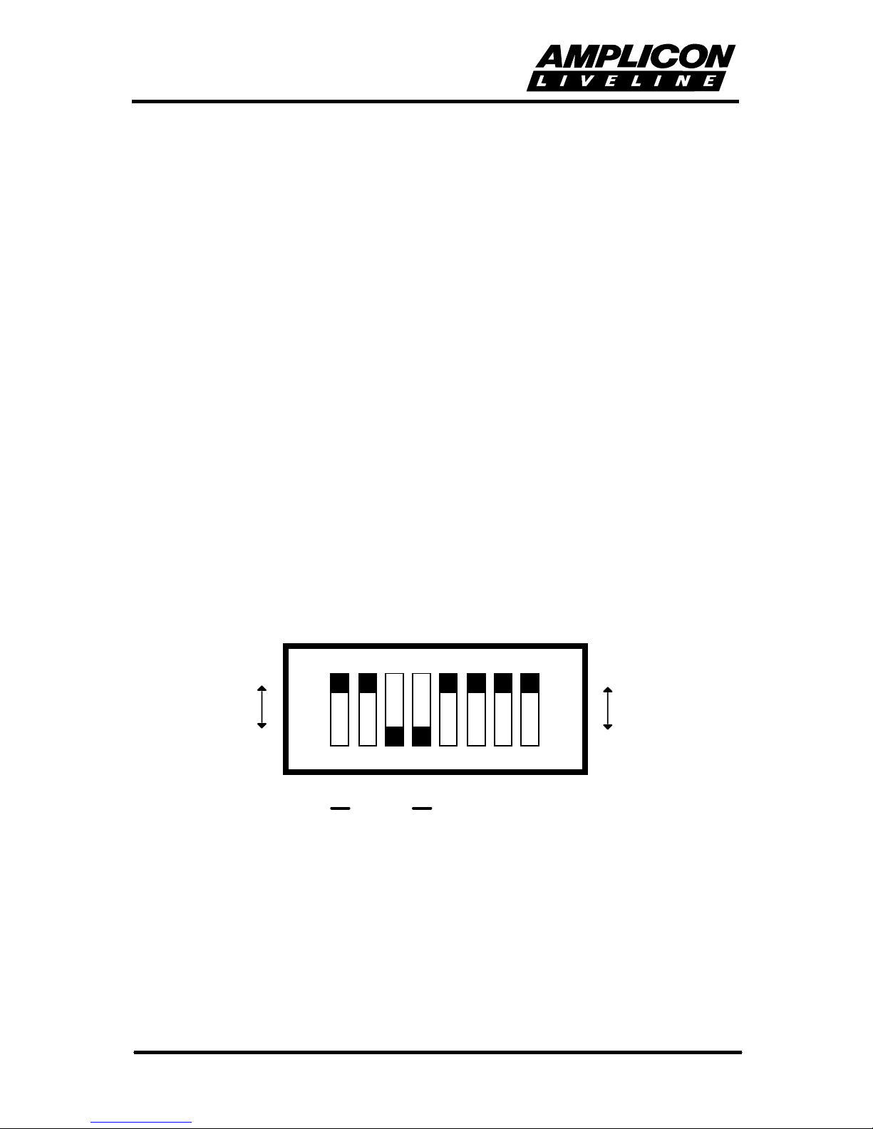
There are six Interrupt Request levels available on the PC27E, IRQ2 - IRQ7 with IRQ2 having
highest priority and IRQ7 the lowest priority. The interrupt level is selected by the position of
jumper J5, and, when selected, an interrupt will be sent to the 8259 interrupt controller inside
the computer at that level on the falling edge of /BUSY from the A/D converter (ie at the end
of a conversion - see section 6.4).
4.4 Counter/Timer Clock Selection
4.4.1 Timing for A/D Conversion
The 4MHz on-board clock signal is used as the source for the Counter/Timer. Any one of the
three outputs of the Counter/Timer can be connected to the /TIM input of the PAL. A falling
edge of /TIM will trigger an A/D conversion.
Jumpers J2, J3 and J4 may be positioned according to the required frequency of /TIM. The
connections to these jumpers, showing the factory configuration, are given in figure 2.
The 4MHz clock is the input to Counter 0, who’s output can be jumpered to /TIM or cascaded
to the Counter 1 clock input, through Jumper J2 (see fig 2). If cascaded, the output of Counter
1 can be connected to /TIM, by positioning J3 in the upper position, or cascaded to the
Counter 2 clock input by positioning J4 in the upper position. If cascaded the output of
Counter 2 can be connected to /TIM by positioning J3 in the lower position.
An external TTL compatible signal connected to SK1 pin 1 can be used as an alternative
clock input to Counter 2 by positioning J4 in the lower position.
4
/5
6
4
4
6
4
/5
&(
6
4
!
7$$
6
FIG.2 CONNECTIONS TO COUNTER/TIMER JUMPERS

PC27E Page 11
4.4.2 Frequency Measurements
A simple Frequency Counter can be implemented using the external frequency output on
connector SK1 pin 1.
The output of Counter 0 is inverted by QA12-B, and then fed to the gate of counter 2 by
positioning jumper J7 to /OUT0 (upper position). Therefore Counter 0 controls the gate of
Counter 2 and, if Counter 0 is programmed for Mode 2 (terminal count), a fixed-length gate
pulse can be created for Counter 2.
The external signal (of unknown frequency) can be connected to SK1 pin 1 and jumpered into
the clock of counter 2 by positioning J4 in the lower position. If programmed to count down
from HexFFFF, Counter 2 will count the number of external clock cycles during its gate pulse.
Since the gate pulse is of known duration, the number of external clock cycles per second can
be calculated, and hence the frequency.
4.5 Wait State Generator Setting (Option)
The PC27E incorporates an on-board wait state generator (QA10) to enable it to operate
reliably in a wide range of PC/XT/AT and ISA machines. The need for this is because some
machines, that are otherwise IBM compatible, now operate the I/O expansion bus at clock
frequencies higher than the 8MHz specified in the ISA standard. This option is not fitted as
standard.
Many interface ICs currently available cannot operate at these higher frequencies and it
becomes necessary to slow down the bus interface signals, locally, on the PC27E board. The
degree of retardation can be adjusted to give optimum performance in any machine. Being
local to the PC27E board, this slowing down in no way impairs the performance of the host
computer.
The expansion bus frequency is not necessarily the same as that of the main processor clock.
A computer which is specified as a 12 or 16 MHz machine could well have an expansion bus
frequency of 8MHz. Unless explicitly stated in the machine specification there is no easy way
to establish the speed of the expansion bus. If the expansion speed is known, then use Table
2 to set the appropriate number of wait states. If the bus speed is not known, it is suggested
that the number of wait states is left at zero (No jumper). If the PC27E functions correctly
leave the setting at zero wait states. If operation is erratic, increase the number of wait states.
Introducing wait states can cause some machines to hang up, otherwise no harm can be
done by setting the number of wait states too high, however the response of the PC27E board
will not be optimum.
82!
!
9&!
4&
4%:;
%:;
%:;
:;0"+1
664&'
<)#
2
2
2
TABLE 2 SETTINGS FOR WAIT STATE GENERATOR

Page 12 PC27E
4.6 Input Voltage Range Setting
The analog input voltage range can be set by the position of jumper J1. Table 3 shows the
settings for the PC27E.
J1 JUMPER
POSITION
INPUT VOLTAGE RANGE
PC27
0 to +4v
-2 to +2v
-4 to +4v
UP
BP
No Jumper
TABLE 3 ANALOG INPUT VOLTAGE RANGE SETTINGS
4.6.1 Input Attenuators
Although the PC27E has pre-defined input ranges, these can be modified on a
channel by channel basis to allow higher or intermediate input voltages to be handled.
This is accomplished by drilling out a link from the required channel and inserting
appropriate resistors. Each channel is provided with a position for an input series
resistor and single in-line resistor networks for two groups of eight channels.
PLEASE NOTE. IF PROPERLY UNDERTAKEN, THESE MODIFICATIONS WILL
NOT INVALIDATE THE WARRANTY. NO MODIFICATION SHOULD BE MADE TO
A PC27E UNDER EVALUATION.
QA5, QA7
INPUT
MULTIPLEXERS RN4, RN5
RN2, RN3 Vin
PC27E
SK1
The links corresponding to each input channel are as follows, and can be located using the
diagrams shown in figures 7 and 8, the printed circuit board layouts.

PC27E Page 13
Channel Input Pin Attenuator Resistor Positions
Nº SK1 Input Ground
0 4 RN2 - A RN4 pin 2
1 5 RN2 - B RN4 pin 3
2 6 RN2 - C RN4 pin 4
3 7 RN2 - D RN4 pin 5
4 8 RN2 - E RN4 pin 6
5 9 RN2 - F RN4 pin 7
6 10 RN2 - G RN4 pin 8
7 11 RN2 - H RN4 pin 9
8 12 RN3 - A RN5 pin 9
9 13 RN3 - B RN5 pin 8
10 14 RN3 - C RN5 pin 7
11 15 RN3 - D RN5 pin 6
12 16 RN3 - E RN5 pin 5
13 17 RN3 - F RN5 pin 4
14 18 RN3 - G RN5 pin 3
15 19 RN3 - H RN5 pin 2
For example, to obtain a range of ±25 volts on analog input channel 0, while retaining ranging
of ±2 volts on the other 15 channels:
1. Insert a single in-line resistor network in position RN4. 100kΩwould be a
suitable value. (If only one channel is to be equipped with an attenuator, then a single
100kΩresistor can be inserted between RN4 pins 1 and 2).
2. Drill out the drill point at RN2 - A using a 1mm drill, leaving the position clear
to insert a resistor.
3. Calculate the required input resistor, Rin, thus:-
The maximum input voltage to the multiplexer must be ±2 volts for a full scale
reading, with Vin ±25 volts maximum.
Full scale reading 100k
---------------------------------- = ---------------
Maximum input voltage 100k + Rin
( Maximum input voltage )
Rin = (100k x ----------------------------------- ) - 100k
( Full scale reading )
Rin = (100k x 25/2 ) - 100k = 1.15MΩ
4. Insert a 1.15MΩhigh stability resistor in the position vacated by drilling out
RN2 - A.

Page 14 PC27E
5. ELECTRICAL CONNECTIONS
5.1 User Connections
Inputs and Outputs to the PC27E are connected via a 37-way D socket on the PC27E card
mounting bracket and marked SK1. Be careful to observe pin numbering.
FIG. 3 CONNECTOR SK1 PIN DESIGNATIONS
5.2 EMC Considerations
In order to maintain compliance with the EMC directive, 89/336/EEC, it is mandatory that the
final system integrator uses good quality screened cables for external connections. It is up to
the final system integrator to ensure that compliance with the Directive is maintained.
Amplicon Liveline offers a series of good quality screened cables for this purpose. Please
contact our sales staff.
EXT TRIG
120
221
322
423
524
6
26
25
7
27
8
28
9
10 29
30
11
31
12
32
13
33
14
34
15
35
16
36
17
18 37
19
EXT CL
K
CHN14
CHN15
AGND
CHN0
CHN1
CHN2
CHN3
CHN4
CHN5
CHN6
CHN7
CHN8
CHN9
CHN10
CHN11
CHN12
CHN13
GND
AGND
GND
AGND
AGND
AGND
AGND
AGND
AGND
AGND
AGND
AGND
AGND
AGND
AGND
AGND
AGND
AGND

PC27E Page 15
5.3 Main I/O Bus Backplane Connections
Connection to the computer is made through the I/O channel main bus. The pin designations
are shown in Figure 4, but for further information please consult the technical reference
manual for the host computer.
62 Pin Connector (Pins B1 and A1 are at the bracket end of the board)
Ground < B1 A1 < -I/O CHCK
+ Reset< B2 A2 < > SD7
+5 Volts< B3 A3 < > SD6
+IRQ2/9* > B4 A4 <SD5
-5 Volts < B5 A5 < > SD4
+DRQ2 > B6 A6 < > SD3
-12 Volts< B7 A7 < > SD2
-0WS < > B8 A8 < > SD1 C
+12 Volts< B9 A9 < > SD0 O
Ground < B10 A10 < I/O CHRDY M
S -SMEMW< B11 A11 < > AEN P
O -SMEMR< B12 A12 < > SA19 O
L -IOW < > B13 A13 < > SA18 N
D -IOR < > B14 A14 < > SA17 E
E -DACK3< > B15 A15 < > SA16 N
R +DRQ3 < > B16 A16 < > SA15 T
-DACK1< > B17 A17 < > SA14
S +DRQ1 < > B18 A18 < > SA13 S
I -DACK0< > B19 A19 < > SA12 I
DCLK<>B20 A20 < > SA11 D
E+IRQ7<>B21 A21 < > SA10 E
+IRQ6 < > B22 A22 < > SA9
+IRQ5 < > B23 A23 < > SA8
+IRQ4 < > B24 A24 < > SA7
+IRQ3 < > B25 A25 < > SA6
-DACK2< > B26 A26 < > SA5
+T/C < B27 A27 < > SA4
+BALE < B28 A28 < > SA3
+5 Volts< B29 A29 < > SA2
OSC < B30 A30 < > SA1
Ground < B31 A31 < > SA0
* Note: Pin B4 is IRQ2 for an XT
Pin B4 is IRQ9 for an AT which is re-directed as IRQ2
FIG. 4 - MAIN PC BUS BACKPLANE CONNECTOR PIN ASSIGNMENTS

Page 16 PC27E
6. PROGRAMMING
The PC27E is supplied with a 31/2 inch diskette containing Windows DLLs with Microsoft Visual Basic
example programs, and a Borland Turbo Pascal DOS demonstration program. See Section 2.4 to
find out how to install the software onto your hard disk.
6.1 Windows DLLs and Visual Basic Example Programs
Having installed the software, you will find a number of Windows Dynamic Link Libraries
(DLLs) each of which supports one basic Input/Output function available with the Amplicon
low-cost Data Acquisition boards. Each DLL comes with a Visual Basic example program,
and all the source files for these Visual Basic programs are provided. Any number of these
programs can be run concurrently to build up the system represented by one or more of the
boards being used.
The default installation for the PC27E creates four new icons in the ‘Amplicon Introductory
DLLs’ folder/Program Manager group:
AD27DEMO - Visual Basic analog input demo program
TC53DEMO - Visual Basic timer/counter demo program
README - User Guide for the Amplicon Introductory DLLs
AMPLICON LIVELINE LTD - What Amplicon offers you
To open any of these objects, simply double-click the mouse on the relevant icon.
For more information on the functions provided by the DLLs, and how to use them in your own
Visual Basic Windows programs, please read the User Guide by double-clicking on the
README icon.
6.2 Pascal Demonstration Program
Two Turbo Pascal files are also installed into the Introductory DLL directory:
PC27.PAS (source code)
PC27.EXE (executable)
To run the program log on to the disk drive or directory containing the software and type
PC27 <RETURN>.
On running the program, the screen lists a menu from which the required demonstrations can
be selected. The menu items comprise:
1. Change PC27E base address (Default 300Hex)
2. S/W controlled sampling on one channel only
3. S/W controlled sampling on 16 channels
4. Interrupt controlled sampling on one channel only
5. Interrupt controlled sampling on 16 channels
6. External trigger controlled sampling on one channel

PC27E Page 17
7. Frequency Counter
8. EXIT to DOS
6.3 Copyright
The software on the demonstration disk is copyright Amplicon Liveline Ltd. Any user who has
purchased a PC27E may use the software, or any part of it, for use in his own programs, or
for resale when delivered with a PC27E.
6.4 Programming the 82C53 Counter/Timers
The three counter/timers of the 82C53 can be independently programmed to operate in any
one of six modes. These are:
1. Mode 0: Interrupt on Terminal Count.
2. Mode 1: Programmable One Shot.
3. Mode 2: Rate Generator.
4. Mode 3: Square Rate Generator.
5. Mode 4: Software Triggered Strobe.
6. Mode 5: Hardware Triggered Strobe.
Details of the operation of these various modes are contained in Appendix 82C53.
The function of a particular timer/counter is established by writing a control word to the control
register. This 8 bit word consists of four fields as follows:
D7 D6 D5 D4 D3 D2 D1 D0
Select Read/ Load Select Mode BCD or
Counter Binary
D0 = 0: binary selected.
= 1: BCD selected.
D3,D2,D1 = 0 0 0: Mode 0 selected.
= 0 0 1: Mode 1 selected.
= 1 0 1: Mode 5 selected.
D5,D4 = 0 0: Latch Counter.
= 0 1: Read/Load of LSB only
= 1 0: Read/Load of MSB only
= 1 1: LSB followed by MSB
D7,D8 = 0 0: Counter 0 selected.
= 0 1: Counter 1 selected.
= 1 0: Counter 2 selected.
= 1 1: Prohibited combination.

Page 18 PC27E
Example 1
To select Counter 1 to Mode 3, loading/reading low order byte followed by high order byte in
binary, the control word is:
0 1 1 1 0 1 1 0 = 76 hex
This value has to be loaded to the control register whose address is Base Address + 07.
Assuming that the board base address is 0300, the following BASICA or QuickBASIC
statement will load the control register with 76 hex.
OUT &H0307, &H76
The value of the count has now to be loaded to the counter. The address of Counter 1 is base
address +05 which, in our example would be 0305. To load the value 50 decimal to this
counter the Turbo Pascal statements
Port[$305] := $32;
Port[$305] := 0;
are used.
It should be noted that both the low order and high order bytes have to be loaded even though
the high order byte, as in the above example, is zero.
Example 2
To read the current count on Counter 1 without affecting the counting operation the counter
has to be latched. To do this the control word 0 1 0 0 0 1 1 0 (46 hex) is loaded to the control
register by OUT &H0307, &H46
The two bytes then have to be read from the latch using the command
n = INP( &H0305 )
to read the low order byte followed by
n = INP( &H0305 )
to read the high order byte. The two bytes MUST be read before attempting to execute
another OUT instruction on the same counter.
6.5 Programming the 7870 A/D Converter
There is no need for software programming of the A/D mode since the operational conditions
are set up in the hardware on the PC27E. The 7870 is wired for Mode 1 operation, with
parallel output format in two bytes.
A conversion is initiated by a low going pulse on /CONVST, which is generated by the PAL
whenever START (BA +2 write) is addressed. At the end of a conversion /BUSY goes low,
generating an IRQ, if selected. A read operation to the 7870 accesses the data and the
/BUSY line is reset high again.
To access the data, two read operations are required. The HBE pin selects which byte of data
is to be read; when low (BA+0 read) the lower 8 bits are placed on the data bus, when high
(BA + 1 read) the upper 4 bits of the 12 bit word are placed on the data bus. These 4 bits are
right justified and thereby occupy the lower nibble of the data byte, while the higher nibble
contains zeros.

PC27E Page 19
The 12 bit data word is not coded in pure binary, but in a form of 2s complement where the
most significant bit is inverted. The transfer functions for bipolar and unipolar operation are
given in figure 5.
N.B. Under software sampling it is not possible to detect the status of each sample, so
the user must insert a delay between starting the conversion and reading the first byte,
typically >10µs.
===>
===>
===>
===>
===>
===>
===>
===>
===>
1
&47!
4
&
4
/
*3(> -
>(
?(@
.#
#0A#
)0$%.0
===>
===>
===>
===>
===>
===>
===>
===>
&47!
4
&
4
/
3>
?(@
40.#
#0A#
)0$%.0
1
FIG. 5 ANALOG TO DIGITAL CONVERTER OUTPUT CODE
6.6 Programming Hints
6.6.1 Settling Time of Input Stages
When switching to another analog input channel, the settling time of the multiplexer plus the
amplifier stages is less than 10 µSecs to within 0.1% of full scale. As the A to D Converter
incorporates a sample and hold circuit, careful programming can allow the analog settling
time to overlap A to D conversion time for maximum throughput.

Page 20 PC27E
6.6.2 Aliasing
Never try to sample a signal at a rate less than or equal to twice the signal frequency.
Otherwise distortion known as aliasing will arise where the frequency of the sample data will
appear to be much less.
Aliasing is illustrated in the following diagram.
@
&4
!
!&
!!
!
6.6.3 Inherent Offset in ±4 Volt Bipolar Mode
There is no facility to adjust the offset to zero in ±4 volts, bipolar mode. This gives rise to a
possible offset error of a few millivolts on this range.
If necessary the offset could be compensated in software by subtracting the offset value from
each sample data.
6.6.4 Multiplexer Inputs
Please note that all unused analog input channels must be grounded. The maximum signal
voltage applied to any multiplexer input must not exceed ±5 volts.
6.7 Calibrating the PC27E
6.7.1 Unipolar Calibration
1. Run the PC27E Pascal demonstration program
2. From the main menu, press 2 to select Software Controlled sampling on one channel
only .
3. Enter 1 for unipolar Input and confirm.
4. Enter 1 for the channel number. (Note in the Pascal demo program, the channels are
numbered 1 to 16).
Table of contents
Popular Media Converter manuals by other brands

OST
OST OmniConverter GPoE/S user manual

SignaMax
SignaMax 065-1196A user guide

Pro-Ject Audio Systems
Pro-Ject Audio Systems DAC Box USB Instructions for use

ORiNG
ORiNG IGPMC-111GP Quick installation guide

Transition Networks
Transition Networks Milan Raven Series user guide

PureTools
PureTools PT-SP-HD24DA user manual

PROception
PROception PRODMHD11 Installation & configuration manual

Resi
Resi Server-Grade Decoder Setup instructions

Speaka Professional
Speaka Professional SP-5634440 operating instructions

ICP DAS USA
ICP DAS USA I-7565M-HS quick start

Yuan
Yuan SC601 user guide

Treasure Cove
Treasure Cove VIBRA-PHONE 280 manual