User Guide EVAL-AD4858
EVALUATION BOARD HARDWARE
analog.com Rev. 0 | 4 of 14
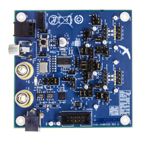
The AD4858 is a fully buffered, 8-channel simultaneous sampling,
20-bit 1 MSPS DAS with differential, wide common mode range
inputs. The AD4858 has an on-chip low drift 4.096 V internal volt-
age reference, but, optionally, it also accepts an external reference
applied through the REFIO pin and provided on-board (LTC6655).
The device operates from different power rails, provided through
on-board LDOs as described in Power Supplies section. An option
to connect external supplies exists and is explained in Table 1.
HARDWARE LINK OPTIONS
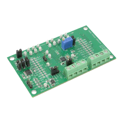
Table 1 details the link option functions and the default power link
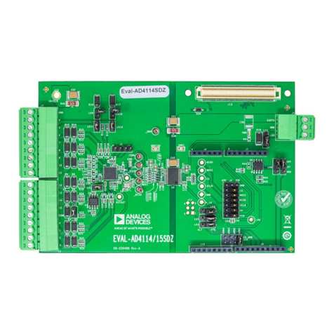
options. The EVAL-AD4858FMCZ can be powered from different
sources, as described in the Power Supplies section. By default,
the power supply required for the EVAL-AD4858FMCZ comes from
the ZedBoard controller board. The power supply is regulated by
the on-board regulators that generate the required bipolar supplies.
Table 1. Jumper Details with Factory Default Setting
Link Default Position Function
JODIFF to J7DIFF Not inserted Offset Calibration Jumper. Inserting the JODIFF to J7DIFF jumper link allows short-circuiting the corresponding pair of
inputs in order to measure the AD4858 offset and/or perform and offset calibration.
J0+ to J7+ Not inserted Analog Input to Ground Connection. Insert the J0+ to J7+ jumper link to connect to the AGND pin, the corresponding
positive analog input.
J0− to J7− Not inserted Analog Input to Ground Connection. Insert the J0− to J7− jumper link to connect to the AGND pin, the corresponding
negative analog input.
JV12V A The JV12V link selects the power supply source for the evaluation board.
In Position A, the unregulated supply to the on-board LDOs is taken from the ZedBoard 12 V supply.
In Position B, the unregulated external supply to the on-board LDOs is taken from the V12V_EXT connector.
JSHIFT A The JSHIFT link selects the power supply type for the AD4858.
In position A, the VCC pin = +24 V and the VEE pin = −24 V.
In position B, the VCCpin = +44 V and the VEE pin = −4 V.
If not inserted, the VCC pin = +24 V and the VEE pin = −4 V.
JVCC A The JVCC link selects the VCC pin supply source.
In position A, the VCC pin is provided by the on board LT8330 DC/DC converter.
In position B, the VCC pin is provided though VCC_EXT connector.
JVEE A The JVEE link selects the VEE pin supply source.
In position A, the VEE pin is provided by the on board LT8330 DC-to-DC converter.
In position B, the VEE pin is provided though VEE_EXT connector.
JVDDH A The JVDDH link selects the VDDH pin supply source.
In position A, the VDDH pin is provided by the on board LT1761 2.5 V LDO.
In position B, the VDDH pin is provided though VDDH_EXT connector.
If not inserted, VDDH pin can be tied to the AGND pin by inserting an R40 resistor. To disable the internal LDO, tie the VDDH
pin to the GND pin. With the regulator disabled, connect the VDDL pin to an external supply in the range of 1.71 V to 1.89 V
through the JVDDL link.
JVDD A The JVDD link selects the VDD pin supply source.
In position A, the VDD pin is provided by the on board LT1761 5 V LDO.
In position B, the VDD pin is provided though VDD_EXT connector.
JVDDL Not inserted The JVDDL link selects the VDDL pin supply source.
In position A, the VDDL pin is provided by the on-board LT1761 1.8 V LDO. To use this configuration, tie the VDDH pin to
ground through the JVDDH link.
In position B, the VDDL pin is provided though the VDDL_EXT connector. To use this configuration, tie the VDDH pin to
ground through the JVDDH link.
If not inserted, the internal LDO is used for the JVDDH link to be in position A or B.
JVIO Not inserted The JVIO link selects the VIO pin supply source. If not inserted, the VIO pin is taken from the ZedBoard (default).
Alternatively, the VIO pin can be supplied from either the on-board LDOs or an external supply.
In position A, the VIO pin is provided by the on board LT1761 LDO with an output voltage dependent on the JVIO_LDO link.
The R66 resistor (shown in Figure 20) is unsoldered.
In position B, the VIO pin is provided though VIO_EXT connector. The R66 resistor is unsoldered.
Note the field programmable gate array (FPGA) image provided works at 2.5 V digital level, so use caution when changing
the default position of the JVIO link jumper.
