THine THC63LVD1023B User manual

THAN0185_Rev.1.20_E
1/11
Copyright(C)
2016 THine Electronics, Inc.
THine Electronics, Inc.
Security E
THC63LVD1023B / THC63LVD1024 Evaluation Kit
LVDS Dual Link Evaluation Board
Parts Number: THEVA1023B, THEVA1024
1. General Description
THEVA1023B and THEVA1024 are designed to evaluate THC63LVD1023B/THC63LVD1024 for
transmission video data.
THC63LVD1023B and THC63LVD1024 chipset can transmit 67bit data via dual channel LVDS.
The maximum input clock frequency of THC63LVD1023B is 160MHz, and the maximum output clock
frequency of THC63LVD1024 is 135MHz at Dual in / Single out mode.
2. Features
Common Features
・Low power single 3.3V CMOS design
・Power down mode
・Wide dot clock range suited for TV signal(480i to 1080p), PC signal(VGAto QXGA)
・PLL requires no external components
・Clock edge selectable
THC63LVD1023B
・Single/Dual TTL in, Single/Dual LVDS out
・Double Edge Input(Single in/Dual out Mode)
・Input Port Switch for Single TTL in/Dual out
・Asynchronous Dual TTL in / Dual LVDS out
・3 LVDS Data Mapping Modes
・Pseudo Random Pattern Generation Circuit
・Support Reduced Swing LVDS for Lower EMI
・LQFP 144 Pin
THC63LVD1024
・Single/Dual LVDS in, Single/Dual TTL out
・Double Edge Output
・50% Output Clock Duty Cycle
・TTL Clock Output Timing Programmable
・2 Output Data Mapping Modes
・LQFP 144 pin + Exposed Pad
3.Overview
(a)THEVA1023B (b)THEVA1024
Figure 1 THEVA1023B and THEVA1024
Downloaded from Arrow.com.
2/11
THAN0185_Rev.1.20_E
Copyright(C) 2016 THine Electronics, Inc.
THine Electronics, Inc.
Security E
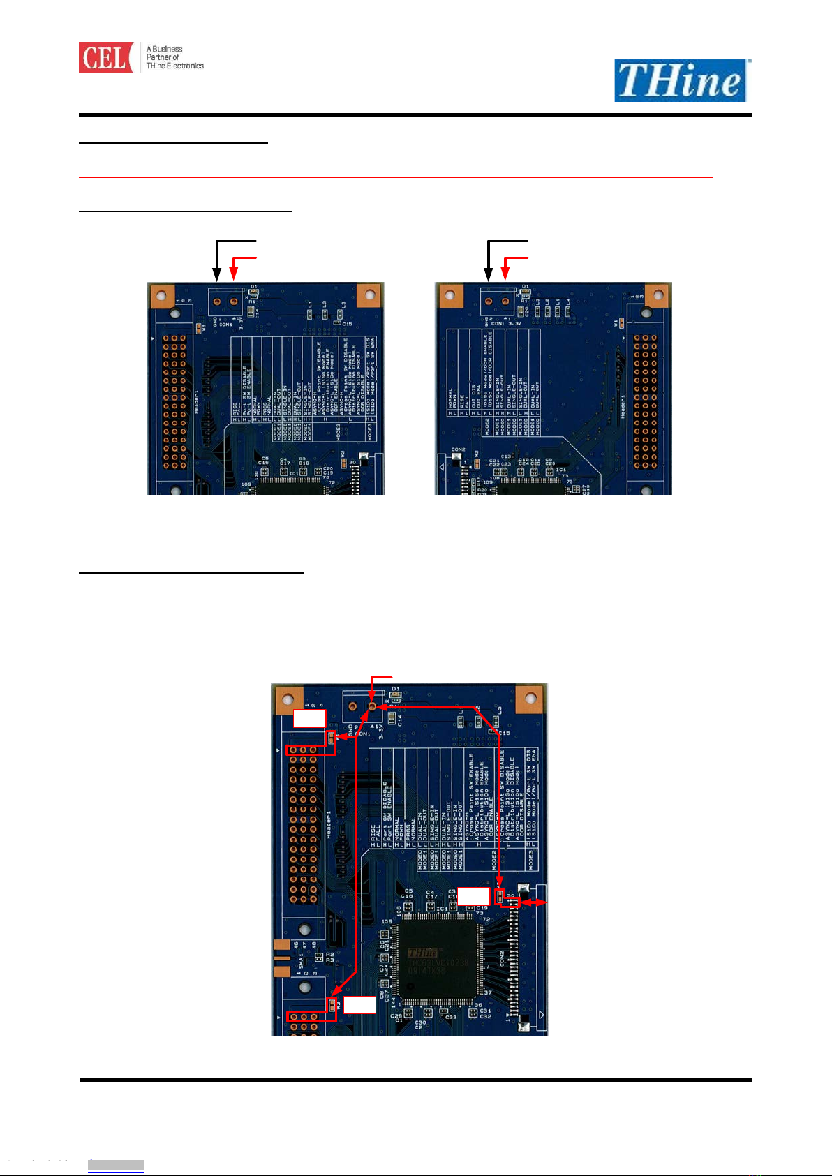
2. Power Supply Setup
This chapter shows power supply condition.
Caution: Please check if there is no power-GND short on below red trace before supplying any power.
3.3V Power Supply to Each Board
Each evaluation board requires 3.3V power supply. Please use “CON1” connector typically.
(a)THEVA1023B (b)THEVA1024
Figure 2 Power Supply for Evaluation Board
Power Supply from / to Connector
3.3V power supply can be connected to Header1 and CON2 by using W1, W2 and W3solder jumper.
THEVA1023B
W1: Connect the 3.3V power supply with pin#1, 2 and 3 of Header1.
W2: Connect the 3.3V power supply with pin#13 and 14 of CON2.
W3: Connect the 3.3V power supply with pin#1, 2 and 3 of Header2.
Figure 3 THEVA1023B Power Supply from / to Each Connector
3.3V Power Supply
Ground
3.3V Power Supply
Ground
W1
W2
W3
Downloaded from Arrow.com.Downloaded from Arrow.com.
3/11
THAN0185_Rev.1.20_E
Copyright(C) 2016 THine Electronics, Inc.
THine Electronics, Inc.
Security E
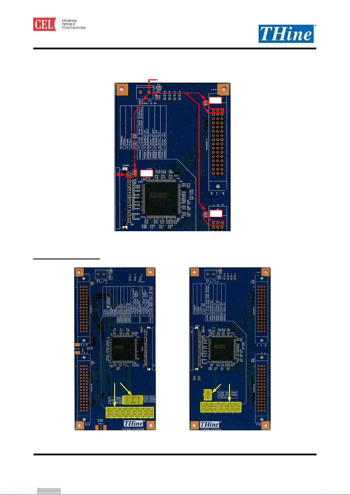
THEVA1024
W1: Connect the 3.3V power supply with pin#1, 2 and 3 of Header1.
W2: Connect the 3.3V power supply with pin#1 and 2 of CON2.
W3: Connect the 3.3V power supply with pin#1, 2 and 3 of Header2.
Figure 4 THEVA1024 Power Supply from / to Each Connector
3. Function Setting
Setting pin of each board is shown in yellow area of Figure 5.
(a)THEVA1023B (b)THEVA1024
Figure 5 Position of Function Setting Pin
W1
W2
W3
Setting pin
Setting pin
Downloaded from Arrow.com.Downloaded from Arrow.com.Downloaded from Arrow.com.

4/11
THAN0185_Rev.1.20_E
Copyright(C) 2016 THine Electronics, Inc.
THine Electronics, Inc.
Security E
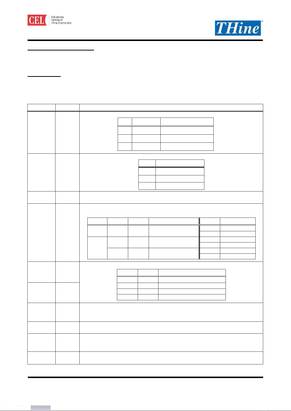
Pin#2 of each 3HEADER is connected to IC’s setting pin.
Each setting pin’s high or low setting can set by connecting pin#2 of 3HEADER and high level or low level.
(a)3HEADER Description (b)High Level Setting (c)Low Level Setting
Figure 6 High / Low Setting Description
THEVA1023B and THEVA1024 have 3 level setting pin.
Please refer to Figure 7 to set the pin into each level.
Figure 7 Description of 3Level Setting Pin
(a) High Level Setting (b) Middle Level Setting (c) Low Level Setting
Figure 8 High / Middle / Low Setting Description
4. Clock Input from SMA Connector
THEVA1023B can also choose the TTL clock input from SMA connector by using 0ohm resistor. If you want
to use SMAconnector for clock input, please change the 0ohm resistor mount from R2 to R3, and R4 to R5.
(a)External Clock Input for Channel1 (b)External Clock Input for Channel2
Figure 9 TTL Clock Input Connector Select
2. Connected with
IC’s setting pin
1. High level
3. Low level
High setting
Low setting
Connected with
IC’s setting pin
1. High level
3. Low level
2. Middle level
High setting
Middle setting
Low setting
Clock input from Header1
(default)
Clock input from SMA1
Clock input from Header2
(default)
Clock input from SMA2
Downloaded from Arrow.com.Downloaded from Arrow.com.Downloaded from Arrow.com.Downloaded from Arrow.com.
5/11
THAN0185_Rev.1.20_E
Copyright(C) 2016 THine Electronics, Inc.
THine Electronics, Inc.
Security E
5. Status Indicate LED
LED “D1” indicates 3.3V power supply status.
6. Function
This chapter shows function setting of THEVA1023B and THEVA1024.
Table 1THEVA1023B Function Setting Description
Silk
Symbol
Function
RS RS
LVDS swing mode, VREF select.
RS LVDS Swing Small Swing Input Support
VIHM 350mV N / A
VIMM 350mV RS = VREF
VILM 200mV N / A
MAP MAP
LVDS mapping table select
MAP Mapping Mode
VIHM Mapping MODE1
VIMM Mapping MODE2
VILM Mapping MODE3
MODE3 MODE3
Input port switching function enable when MODE[1:0] = H, L(Single-in / Dual-out).
H or Open: Port Switch Disable L: Port Switch Enable
MODE2 MODE2
The use of this function depends on the setting of MODE[1:0] or ASYNC.
ASYNC MODE1 MODE0 Function MODE2 Enable / Disable
H x x
Cross Point
Switching
H
Enable
L
Disable
L H H
Distribution
Function
H
Enable
L
Disable
H L
DDR(Double Edge Input)
Function
H
Enable
L
Disable
MODE1 MODE1
Pixel data mode select
MODE1
MODE0
Function
L
L
Dual Link (Dual-in / Dual -out)
L
H
Single Link (Dual-in / Single-out)
H
L
Dual Link (Single-in / Dual -out)
H
H
Single Link (Single-in / Single-out)
MODE0 MODE0
ASYNC ASYNC Asynchronous function.
H : Asynchronous Function Enable (MODE[1:0] function is enabled in this setting)
L : Asynchronous Function Disable (MODE[1:0] function is disabled in this setting)
R/F R/F
Input clock triggering edge select.
H : Rising Edge L : Falling Edge
PRBS PRBS
PRBS (Pseudo Random Binary Sequence) generator is active in order to evaluate eye
diagram when MODE[1:0] = L, L (Dual-in / Dual-out) or ASYNC = H.
H : PRBS Generator Enable L : Normal Operation
PDWN PDWN
Power down function setting
H : Normal Operation L : Power Down Mode (All outputs are Hi-Z)
Downloaded from Arrow.com.Downloaded from Arrow.com.Downloaded from Arrow.com.Downloaded from Arrow.com.Downloaded from Arrow.com.

6/11
THAN0185_Rev.1.20_E
Copyright(C) 2016 THine Electronics, Inc.
THine Electronics, Inc.
Security E
Table 2 THEVA1024 Function Setting Description
Silk
Symbol
Function
DK DK
LVDS swing mode, V
REF
select.
MODE1 MODE0 DK Function
L L
H L
H H
L 0
M -6(tDOUT)/28
H 6(tDOUT)/28
L H
L 0
M -7(tDOUT)/28
H 7(tDOUT)/28
MODE2 MODE2
DDR function enable. The use of this function depends on the setting MODE[1:0].
MODE1
MODE0
MODE2
Function
L
L
L
Must be tied to GND
L H
H
DDR Function Enable
L
DDR Function Disable
H
L
L
Must be Tied to GND
H
H
L
Must be Tied to GND
MODE1 MODE1
Pixel data mode select
MODE1 MODE0 Function
L
L
Dual Link (Dual-in / Dual -out)
L
H
Dual Link (Dual-in / Single-out)
H
L
Single Link (Single-in / Dual -out)
H H Single Link (Single-in / Single-out)
MODE0 MODE0
OE OE
Output enable
H : Output Enable L : Output Disable
R/F R/F Output clock triggering edge select.
H : Rising Edge
L : Falling Edge
PDWN PDWN
Power down function setting
H : Normal Operation
L : Power Down Mode (All outputs are Hi-Z)
MAP MAP
LVDS mapping table select.
H : Mapping MODE1 L : Mapping MODE2
Downloaded from Arrow.com.Downloaded from Arrow.com.Downloaded from Arrow.com.Downloaded from Arrow.com.Downloaded from Arrow.com.Downloaded from Arrow.com.
7/11
THAN0185_Rev.1.20_E
Copyright(C) 2016 THine Electronics, Inc.
THine Electronics, Inc.
Security E
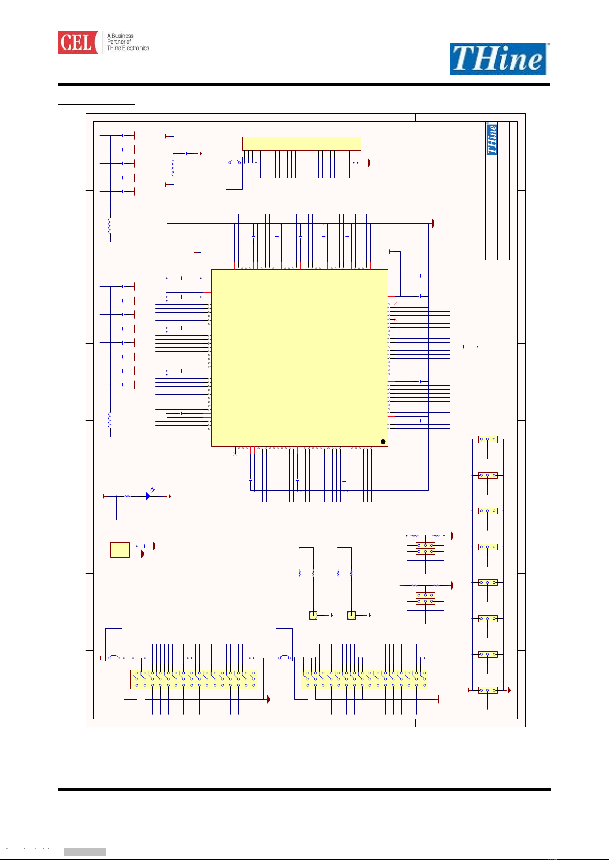
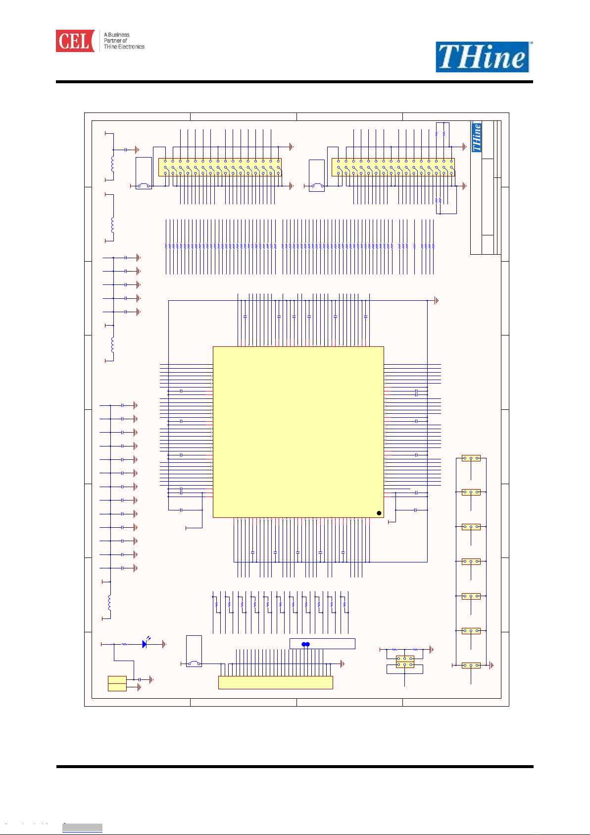
7. Schematic
Figure 10 THEVA1023B Schematic
1
1
2
2
3
3
4
4
5
5
6
6
7
7
8
8
D D
C C
B B
A A
Title
Number RevisionSize
A3
Date: 2015/03/05 Sheet of
File: \\..\THC63LVD1023B.SchDoc Drawn By:
THEVA1023B
1.00
1 1
282836-2(NC)
1
2GND
VCC
CON1
GND 10uF
C14
GND
VDD3.3
SML-310MT
D1
150Ω
R1
GND
VDD3.3
MPZ1608R471A
L1
Inductor
GND
VDD3.3
MPZ1608R471A
L2
Inductor
0.1uF
C10
GND
LVCC
VDD3.3
MPZ1608R471A
L3
Inductor
0.1uF
C15
GND
PVCC
52271-3069(NC)
1
2
3
4
5
6
7
8
9
10
11
12
13
14
15
16
17
18
19
20
21
22
23
24
25
26
27
28
29
30 CON2
TD1+
TD1-
TCLK1+
TCLK1-
TC1+
TC1-
TB1+
TB1-
TA1+
TA1-
VDD3.3
GND
B27
2
VCC
3
GND
4
B28
5
B29
6
HSYNC1
7
VSYNC1
8
DE1
9
HSYNC2
10
VSYNC2
11
DE2
12
VCC
13
GND
14
CLKIN1
15
CLKIN2
16
CONT11
17
CONT12
18
CONT21
19
R/F
21
RS
22
MODE3
23
MAP
24
MODE1
25
MODE0
26
B26
1
MODE2
27
ASYNC
28
CONT22
20
N/C
29
N/C
33
/PDWN
30
PRBS
31
Reserved
32
PGND
34
PVCC
35
PGND
36
TD1+ 58
TD1- 59
TCLK1+ 62
TCLK1- 63
TC1+ 64
TC1- 65
LVCC 67
TB1+ 68
TB1- 69
TA1+ 70
TA1- 71
LGND 72
PGND 73
PVCC 74
R10 76
R11 77
R12 78
R13 79
R14 80
R15 81
VCC 82
GND 83
R16 84
R17 85
R18 86
R19 87
G10 88
G11 89
G12 90
G13 91
G14 92
VCC 93
GND 94
G15 95
G16 96
G17 97
G18 98
G19 99
B10 100
B11 101
B12 102
B13 103
VCC 104
GND 105
B14 106
B15 107
B16 108
N/C
109
B17
110
B18
111
B19
112
VCC
113
GND
114
R20
115
R21
116
R22
117
R23
118
R24
119
R25
120
R26
121
R27
122
R28
123
R29
124
VCC
125
GND
126
G20
127
G21
128
G22
129
G23
130
G24
131
G25
132
G26
133
G27
134
G28
135
G29
136
VCC
137
GND
138
B20
139
B21
140
B22
141
B23
142
B24
143
B25
144
TE1- 57
TE1+ 56
LVCC 61
TD2+ 40
TD2- 41
TCLK2+ 44
TCLK2- 45
TC2+ 46
TC2- 47
LVCC 49
TB2+ 50
TB2- 51
TA2+ 52
TA2- 53
LGND 60
LGND 42
TE2+ 38
TE2- 39
LGND 37
LGND 66
LVCC 55
LVCC 43
LGND 54
LGND 48
PGND 75
IC1
THC63LVD1023B
PCN10-48P-2.54DSA_LEFT(NC)
1
20
2
3
4
5
6
7
8
9
10
11
12
13
14
15
16
17
18
19
30
29
28
27
26
25
24
23
22
21
40
39
38
37
36
35
34
33
32
31
48
47
46
45
44
43
42
41
Header1
VDD3.3
GND
VSYNC1
DE1
CLKIN1_CON
CONT12
G12
G13
G19
G14
G15
G16
G17
G18
G10
G11
B14
B15
B16
B17
B18
B19
B10
B11
B12
B13
R10
R11
R12
R13
R14
R15
R16
R17
R18
R19
HSYNC1
CONT11
PCN10-48P-2.54DSA_LEFT(NC)
1
20
2
3
4
5
6
7
8
9
10
11
12
13
14
15
16
17
18
19
30
29
28
27
26
25
24
23
22
21
40
39
38
37
36
35
34
33
32
31
48
47
46
45
44
43
42
41
Header2
VDD3.3
GND
CONT22
R20
R21
R22
R23
R24
R25
R26
R27
R28
R29
G20
G21
G22
G23
G24
G25
G26
G27
G28
G29
B20
B21
B22
B23
B24
B25
B26
B27
B28
B29
CONT21
0.01uFC21
0.01uFC24
0.01uFC27
0.01uFC29
0.01uFC30
0.01uFC31
0.01uFC16
0.01uFC17
0.01uFC19
0.01uFC18
0.01uFC22
0.01uFC23
0.01uFC25
0.01uFC26
0.01uFC28
PVCC
PVCC
GND
R10
R11
R12
R13
R14
R15
R16
R17
R18
R19
G12
G13
G19
G14
G15
G16
G17
G18
G10
G11
B14
B15
B16
B17
B18
B19
B10
B11
B12
B13
R20
R21
R22
R23
R24
R25
R26
R27
R28
R29
G20
G21
G22
G23
G24
G25
G26
G27
G28
G29
B20
B21
B22
B23
B24
B25
B26
B27
B28
B29
VSYNC1
DE1
HSYNC1
CLKIN1
CONT12
CONT11
CONT22
CONT21
0.1uFC20
0.1uFC32
0.1uF
C2
GND
0.1uF
C3
GND
0.1uF
C4
GND
0.1uF
C5
GND
0.1uF
C6
GND
0.1uF
C7
GND
0.1uF
C8
GND
VCC
0.1uF
C1
VCC0
VCC1
VCC2
VCC3
VCC5
VCC7
VCC4
VCC6
GND
0.1uF
C9
0.1uF
C11
GND
0.1uF
C12
GND
0.1uF
C13
GND
LVCC0
LVCC1
LVCC2
LVCC3
LVCC4
LVCC0
LVCC1
LVCC2
LVCC3
LVCC4
VCC0
VCC1
VCC2
VCC4
VCC3
VCC6
VCC5
VCC7
1
2
3
3HEAD(NC)
Header7
1
2
3
3HEAD(NC)
Header8
1
2
3
3HEAD(NC)
Header9
GND
MODE3 MODE2 MODE1
VDD3.3
TD2+
TD2-
TCLK2+
TCLK2-
TC2+
TC2-
TB2+
TB2-
TA2+
TA2-
TE1-
TE1+
TE2-
TE2+
VSYNC2
HSYNC2
DE2
HSYNC2
VSYNC2
DE2
CLKIN2_CON
PRBS
RS
MODE2
MODE3
MODE1
MAP
MODE0
R/F
ASYNC
PDWN
0.01uFC33
GND
1
2
3
3HEAD(NC)
Header3
1
2
3
3HEAD(NC)
Header10
1
2
3
3HEAD(NC)
Header11
1
2
3
3HEAD(NC)
Header12
1
2
3
3HEAD(NC)
Header13
1
2
3
3HEAD(NC)
Header14
PDWNMODE0 ASYNC R/F PRBS
1
2
3
3HEAD(NC)
Header4
10kΩ
R6
10kΩ
R8
VDD3.3
GND
RS
1
2
3
3HEAD(NC)
Header5
1
2
3
3HEAD(NC)
Header6
10kΩ
R7
10kΩ
R9
VDD3.3
GND
MAP
1
2
SMA103-T16(NC)
SMA1 0Ω(NC)R3
CLKIN1_CON 0ΩR2 CLKIN1
CLKIN1_SMA
GND
CLKIN2
1
2
SMA103-T16(NC)
SMA2 0Ω(NC)R5
CLKIN2_CON 0ΩR4 CLKIN2
CLKIN2_SMA
GND
TB1+
TB1-
TA1+
TA1-
TCLK1+
TCLK1-
TC1+
TC1-
TD1+
TD1-
TE1-
TE1+
TB2+
TB2-
TA2+
TA2-
TCLK2+
TCLK2-
TC2+
TC2-
TD2+
TD2-
TE2-
TE2+
Solder Jumper
W1
Solder Jumper
W2
Solder Jumper
W3
Downloaded from Arrow.com.Downloaded from Arrow.com.Downloaded from Arrow.com.Downloaded from Arrow.com.Downloaded from Arrow.com.Downloaded from Arrow.com.Downloaded from Arrow.com.
8/11
THAN0185_Rev.1.20_E
Copyright(C) 2016 THine Electronics, Inc.
THine Electronics, Inc.
Security E
Figure 11 THEVA1024 Schematic
1
1
2
2
3
3
4
4
5
5
6
6
7
7
8
8
D D
C C
B B
A A
Title
Number RevisionSize
A3
Date: 2015/03/05 Sheet of
File: \\..\THC63LVD1024.SchDoc Drawn By:
THEVA1024
1.00
1 1
282836-2(NC)
1
2GND
VCC
CON1
GND 10uF
C20
GND
VDD3.3
SML-310MT
D1
150Ω
R1
GND
VDD3.3
MPZ1608R471A
L1
GND
VDD3.3
MPZ1608R471A
L2
0.1uF
C15
GND
LVCC VDD3.3
MPZ1608R471A
L3
PVCC
52271-3069(NC)
1
2
3
4
5
6
7
8
9
10
11
12
13
14
15
16
17
18
19
20
21
22
23
24
25
26
27
28
29
30
CON2
RD1+
RD1-
RCLK1+
RCLK1-
RC1+
RC1-
RB1+
RB1-
RA1+
RA1-
0.01uFC40
0.01uFC23
0.1uF
C2
GND
0.1uF
C3
GND
0.1uF
C4
GND
0.1uF
C5
GND
0.1uF
C6
GND
0.1uF
C7
GND
0.1uF
C8
GND
VCC
0.1uF
C1
VCC0
VCC1
VCC2
VCC3
VCC5
VCC7
VCC4
VCC6
GND
0.1uF
C14
0.1uF
C16
GND
0.1uF
C17
GND
0.1uF
C18
GND
LVCC0
LVCC1
LVCC2
LVCC3
LVCC4
VCC0
0.1uF
C9
GND
VCC8
1
2
3
3HEAD(NC)
Header7
1
2
3
3HEAD(NC)
Header8
GND
MODE2 MODE1
VDD3.3
RD2+
RD2-
RC2+
RC2-
RB2+
RB2-
RA2+
RA2-
RE1-
RE1+
RE2-
RE2+
MODE2
MODE1
MAP
R/F
1
2
3
3HEAD(NC)
Header3
1
2
3
3HEAD(NC)
Header9
1
2
3
3HEAD(NC)
Header10
1
2
3
3HEAD(NC)
Header11
1
2
3
3HEAD(NC)
Header12
PDWNMODE0 OE R/F
1
2
3
3HEAD(NC)
Header4
10kΩ
R73
10kΩ
R79
VDD3.3
GND
DK
1
2
3
3HEAD(NC)
Header5
MAP
RB1+
RB1-
RA1+
RA1-
RCLK1+
RCLK1-
RC1+
RC1-
RD1+
RD1-
RE1-
RE1+
RB2+
RB2-
RA2+
RA2-
RC2+
RC2-
RD2+
RD2-
RE2-
RE2+
PVCC
2
Resereved
3
/PDWN
4
MODE0
5
MODE1
6
DK
7
R/F
8
OE
9
MODE2
10
MAP
11
VCC
12
GND
13
R20
14
R21
15
R22
16
R23
17
R24
18
R25
19
VCC
21
GND
22
R27
23
R28
24
R29
25
G20
26
PGND
1
G21
27
VCC
28
R26
20
VCC
29
G24
33
GND
30
G22
31
G23
32
G25
34
G26
35
G27
36
GND 58
GND 59
CGND 62
R10 63
R11 64
R12 65
R14 67
R15 68
R16 69
VCC 70
GND 71
R17 72
R18 73
R19 74
G11 76
G12 77
G13 78
G14 79
VCC 80
GND 81
G15 82
G16 83
G17 84
G18 85
G19 86
B10 87
VCC 88
GND 89
B11 90
B12 91
B13 92
B14 93
B15 94
B16 95
B17 96
VCC 97
GND 98
B18 99
B19 100
HSYNC 101
VSYNC 102
DE 103
CONT11 104
CONT12 105
VCC 106
PVCC 107
PGND 108
LGND
109
RA1-
110
RA1+
111
RB1-
112
RB1+
113
LVCC
114
LGND
115
RC1-
116
RC1+
117
RCLK-
118
RCLK+
119
LVCC
120
LGND
121
RD1-
122
RD1+
123
RE1-
124
RE1+
125
LVCC
126
LGND
127
RA2-
128
RA2+
129
RB2-
130
RB2+
131
LVCC
132
LGND
133
RC2-
134
RC2+
135
LGND
136
LGND
137
LVCC
138
LGND
139
RD2-
140
RD2+
141
RE2-
142
RE2+
143
LGND
144
VCC 57
CONT22 56
CVCC 61
G29 40
B20 41
B23 44
B24 45
VCC 46
GND 47
B26 49
B27 50
B28 51
B29 52
VCC 53
CLKOUT 60
B21 42
VCC 38
GND 39
G28 37
R13 66
CONT21 55
B22 43
GND 54
B25 48
G10 75
EXP PAD
145
IC1
THC63LVD1024
0.01uFC37
100Ω
R16
100Ω
R20
100Ω
R25
100Ω
R29
100Ω
R33
100Ω
R37
100Ω
R41
100Ω
R46
100Ω
R50
100Ω
R54
100Ω
R59
VDD3.3
GND
RD1+
RD1-
RCLK1+
RCLK1-
RC1+
RC1-
RB1+
RB1-
RA1+
RA1-
RD2+
RD2-
RC2+
RC2-
RB2+
RB2-
RA2+
RA2-
RE1-
RE1+
RE2-
RE2+
0.01uFC28 LVCC0
0.01uFC29
0.01uFC32
0.01uFC34
0.01uFC36
LVCC1
LVCC2
LVCC3
LVCC4
0.01uFC24
0.01uFC25
0.01uFC26
0.01uFC41
0.01uFC42
0.01uFC43
VCC4
0.01uFC27
0.01uFC30
0.01uFC31
0.01uFC33
0.01uFC35
0.01uFC39 0.01uFC22
PCN10-48P-2.54DSA_RIGHT(NC)
1
20
2
3
4
5
6
7
8
9
10
11
12
13
14
15
16
17
18
19
30
29
28
27
26
25
24
23
22
21
40
39
38
37
36
35
34
33
32
31
48
47
46
45
44
43
42
41
Header1
R10_C
R12_C
G12_C
VSYNC_C
R14_C
R16_C
R18_C
G14_C
G16_C
G18_C
G10_C
CONT12_C
B14_C
B15_C
B16_C
B17_C
B18_C
B19_C
HSYNC_C
B10_C
B11_C
B12_C
B13_C
CONT11_C
GND
VDD3.3
R20_C
R22_C
G22_C
R24_C
R26_C
R28_C
G24_C
G26_C
G28_C
G20_C
CONT22_C
B24_C
B25_C
B26_C
B27_C
B28_C
B29_C
B20_C
B21_C
B22_C
B23_C
CONT21_C
R21_C
R23_C
G23_C
G29_C
R25_C
R27_C
R29_C
G25_C
G27_C
G21_C
R11_C
R13_C
G13_C
DE_C
G19_C
R15_C
R17_C
R19_C
G15_C
G17_C
CLKOUT_C
G11_C
GND
PCN10-48P-2.54DSA_RIGHT(NC)
1
20
2
3
4
5
6
7
8
9
10
11
12
13
14
15
16
17
18
19
30
29
28
27
26
25
24
23
22
21
40
39
38
37
36
35
34
33
32
31
48
47
46
45
44
43
42
41
Header2
GND
VDD3.3
GND
GND
VCC1
VCC2
VCC3
VCC5
VCC6
VCC7
CVCC
VCC8
VCC9
VCC10
VCC11
VCC12
PVCC
PVCC
VDD3.3
MPZ1608R471A
L4
0.1uF
C19
GND
CVCC
R10
R11
R12
R13
R14
R15
R16
R17
R18
R19
G12
G13
G19
G14
G15
G16
G17
G18
G10
G11
B14
B15
B16
B10
B11
B12
B13
B17
B18
B19
R27
R28
R29
R20
R21
R22
R23
R24
R25
R26
MODE0
PDWN
G20
G21
G22
G23
G24
G25
G26
G27
B20
B21
B22
B23
B24
B25
B26
B27
B28
B29
CONT22
CONT21
CLKOUT
CONT12
CONT11
VCC
OE
VSYNC
DE
HSYNC
R10
R11
R12
R13
R14
R15
R16
R17
R18
R19
G12
G13
G19
G14
G15
G16
G17
G18
G10
G11
B14
B15
B16
B17
B18
B19
HSYNC
B10
B11
B12
B13
CONT11
CONT12
CONT21
CONT22
R20
R21
R22
R23
R24
R25
R26
R27
R28
R29
G20
G21
G22
G23
G24
G25
G26
G27
G28
G29
B20
B21
B22
B23
B24
B25
B26
B27
B28
B29
VSYNC
DE
CLKOUT
R10_C
R11_C
R12_C
R13_C
R14_C
R15_C
R16_C
R17_C
R18_C
R19_C
G12_C
G13_C
G19_C
G14_C
G15_C
G16_C
G17_C
G18_C
G10_C
G11_C
B14_C
B15_C
B16_C
B17_C
B18_C
B19_C
HSYNC_C
B10_C
B11_C
B12_C
B13_C
CONT11_C
CONT12_C
CONT21_C
CONT22_C
R20_C
R21_C
R22_C
R23_C
R24_C
R25_C
R26_C
R27_C
R28_C
R29_C
G20_C
G21_C
G22_C
G23_C
G24_C
G25_C
G26_C
G27_C
G28_C
G29_C
B20_C
B21_C
B22_C
B23_C
B24_C
B25_C
B26_C
B27_C
B28_C
B29_C
VSYNC_C
DE_C
CLKOUT_C
10ΩR2
10ΩR3
10ΩR4
10ΩR5
10ΩR6
10ΩR7
10ΩR8
10ΩR9
10ΩR10
10ΩR11
10ΩR12
10ΩR13
10ΩR14
10ΩR15
10ΩR17
10ΩR18
10ΩR19
10ΩR21
10ΩR22
10ΩR23
10ΩR24
10ΩR26
10ΩR27
10ΩR28
10ΩR30
10ΩR31
10ΩR32
10ΩR34
10ΩR35
10ΩR36
10ΩR38
10ΩR39
10ΩR40
10ΩR42
10ΩR43
10ΩR44
10ΩR45
10ΩR47
10ΩR48
10ΩR49
10ΩR51
10ΩR52
10ΩR53
10ΩR55
10ΩR56
10ΩR57
10ΩR58
10ΩR60
10ΩR61
10ΩR62
10ΩR63
10ΩR64
10ΩR65
10ΩR66
10ΩR67
10ΩR68
10ΩR69
10ΩR70
10ΩR71
10ΩR72
10ΩR81
10ΩR82
10ΩR83
10ΩR84
10ΩR75
10ΩR76
10ΩR77
10ΩR78
G28
G29
0.1uF
C10
GND
VCC9
0.1uF
C11
GND
VCC10
0.1uF
C12
GND
VCC11
0.1uF
C13
GND
VCC12
0.1uFC210.1uFC38
TP1
TP2
DK
0Ω(NC)R86
0Ω(NC)R87
0Ω(NC)R85
0Ω(NC)R88
Solder Jumper
W2
Solder Jumper
W1
Solder Jumper
W3
Downloaded from Arrow.com.Downloaded from Arrow.com.Downloaded from Arrow.com.Downloaded from Arrow.com.Downloaded from Arrow.com.Downloaded from Arrow.com.Downloaded from Arrow.com.Downloaded from Arrow.com.

9/11
THAN0185_Rev.1.20_E
Copyright(C) 2016 THine Electronics, Inc.
THine Electronics, Inc.
Security E
8. Bills of Materials
Table 3 THEVA1023B BOM
Table 4 THEVA1024 BOM
TYPE Value / Part No. Package SPEC Reference No. Q'ty Note
Capacitor 0.1uF 1005 16V
C1, C2, C3, C4, C5, C6, C7, C8, C9, C10, C11, C12, C13, C15,
C20, C32
17
Capacitor 10uF 2012 16V
C14 1
Capacitor 0.01uF 1005 16V
C16, C17, C18, C19, C21, C22, C23, C24, C25, C26, C27, C28,
C29, C30, C31, C33
16
Connector 282836-2(NC) 5mm_pitch 2pin
CON1 1
Connector 52271-3069(NC) 1mm_pitch 30pin
CON2 1
Connector PCN10-48P-2.54DSA_LEFT(NC) 2.54mm_pitch 48pin
Header1, Header2 2
Connector SMA103-T16(NC) 1.6mm PCB End Jack
SMA1, SMA2 2
Header 3HEAD(NC) 2.54mm_pitch ---
Header3, Header4, Header5, Header6, Header7, Header8,
Header9, Header10, Header11, Header12, Header13, Header14
12
IC THC63LVD1023B LQFP144 ---
IC1 1
Inductor MPZ1608R471A 1608 1.2A
L1, L2, L3 3
LED0 SML-310MT 1608 GREEN
D1 1
Resistor 150Ω 1005 0.1W
R1 1
Resistor 0Ω 1005 0.1W
R2, R4 2
Resistor 0Ω(NC) 1005 0.1W
R3, R5 2
Resistor 10kΩ 1005 0.1W
R6, R7, R8, R9 4
TYPE Value / Part No. Package SPEC Reference No. Q'ty Note
Capacitor 0.1uF 1005 16V
C1, C2, C3, C4, C5, C6, C7, C8, C9, C10, C11, C12, C13, C14,
21
Capacitor 10uF 2012 16V
C20 1
Capacitor 0.01uF 1005 16V
C22, C23, C24, C25, C26, C27, C28, C29, C30, C31, C32, C33,
C34, C35, C36, C37, C39, C40, C41, C42, C43
21
Connector 282836-2(NC) 5mm_pitch 2pin
CON1 1
Connector 52271-3069(NC) 1mm_pitch 30pin
CON2 1
Connector PCN10-48P-2.54DSA_RIGHT(NC) 2.54mm_pitch 48pin
Header1, Header2 2
Header 3HEAD(NC) 2.54mm_pitch ---
Header3, Header4, Header5, Header6, Header7, Header8,
10
IC THC63LVD1024 LQFP144 ---
IC1 1
Inductor MPZ1608R471A 1608 1.2A
L1, L2, L3, L4 4
LED0 SML-310MT 1608 GREEN
D1 1
Resistor 150Ω 1005 0.1W
R1 1
Resistor 10Ω 1005 0.1W
R2, R3, R4, R5, R6, R7, R8, R9, R10, R11, R12, R13, R14, R15,
R17, R18, R19, R21, R22, R23, R24, R26, R27, R28, R30, R31,
R32, R34, R35, R36, R38, R39, R40, R42, R43, R44, R45, R47,
R48, R49, R51, R52, R53, R55, R56, R57, R58, R60, R61, R62,
68
Resistor 100Ω 1005 0.1W
R16, R20, R25, R29, R33, R37, R41, R46, R50, R54, R59 11
Resistor 10kΩ 1005 0.1W
R73, R74, R79, R80 4
Resistor 0Ω(NC) 1005 1A
R85, R86, R87, R88 4
Downloaded from Arrow.com.Downloaded from Arrow.com.Downloaded from Arrow.com.Downloaded from Arrow.com.Downloaded from Arrow.com.Downloaded from Arrow.com.Downloaded from Arrow.com.Downloaded from Arrow.com.Downloaded from Arrow.com.

10/11
THAN0185_Rev.1.20_E
Copyright(C) 2016 THine Electronics, Inc.
THine Electronics, Inc.
Security E
9. Set Items
Table 5 Set Items
TYPE Part No.
DC Connector 282836-2
FFC Connector for LVDS Link 52271-3069
FFC 30pin 1mm Pitch for LVDS Link 98267-0475
Pin Header ---
It’s possible to mount these parts on this board and use.
Downloaded from Arrow.com.Downloaded from Arrow.com.Downloaded from Arrow.com.Downloaded from Arrow.com.Downloaded from Arrow.com.Downloaded from Arrow.com.Downloaded from Arrow.com.Downloaded from Arrow.com.Downloaded from Arrow.com.Downloaded from Arrow.com.

11/11
THAN0185_Rev.1.20_E
Copyright(C) 2016 THine Electronics, Inc.
THine Electronics, Inc.
Security E
10. Notices and Requests
Please kindly read, understand and accept this “Noticees and Requests” before using this product.
For the Material:
1. The product specifications described in this material are subject to change without prior notice.
2. The circuit diagrams described in this material are examples of the application which may not always
apply to design of respective customers. THine Electronics, Inc. (“THine”) is not responsible for
possible errors and omissions in this material. Please note if the errors or omissions should be found in
this material, THine may not be able to correct them immediately.
3. This material contains THine’s copyright, know-how or other proprietary. Copying or disclosing of the
contents of this material to any third party without THine’s prior permission is strictly prohibited.
For the Product:
1. This product is solely designed for evaluation purpose, and other purposes including mass production
and distribution are not intended.
2. This product has been solely manufactured for electric design engineers but not for end-users.
3. This product is not radiation-tolerant product.
4. This product is presumed to be used for general electric device, not for applications which require
extremely high-reliability/safety (including medical device concerned with critical care, aerospace
device, or nuclear power control device). Also, when using this product for any device concerned with
control and/or safety of transportation mean, traffic signal device, or other various types of safety
device, such use must be after applying appropriate measures to the product.
5. This product has been designed with the utmost care to accomplish the purpose of evaluation of IC
products manufactured by THine Electronics, Inc., however, THine MAKES NO WARRANTIES OR
REPRESENTATIONS WITH REGARD TO ANY PERFORMANCE OR FUNCTION OF THIS
PRODUCT IN ANY CIRCUMSTANCE.
6. This product has been manufactured with the utmost care in quality control and product reliability,
however, there may be faults or defects with a low but fixed probability, as inevitable phenomenon
concerned with semiconductor manufacturing processes. Therefore, Customers are encouraged to have
sufficiently redundant or error-preventive design applied to the use of the product so as not to have
THine’s product cause any social or public damage. Replacement of the product is only available in
case of obvious defects of mount devices at the point of unpacking the product. Neither replacement
nor failure analysis of the product is available in any other case of defects with the product and/or the
product’s components.
7. Customers are asked, if required, to judge by themselves on whether this product falls under the
category of strategic goods under the Foreign Exchange and Foreign Trade Control Law.
8. Please Note that if infringement of any third party’s industrial ownership should occur by using this
product, THine will be exempted from any responsibility unless it directly relates to the production
process or functions of the product.
9. Developing, designing and manufacturing of Customers’ own products, equipments or system by using
of this product is strictly prohibited in any way.
THine Electronics, Inc.
sales@thine.co.jp
Downloaded from Arrow.com.Downloaded from Arrow.com.Downloaded from Arrow.com.Downloaded from Arrow.com.Downloaded from Arrow.com.Downloaded from Arrow.com.Downloaded from Arrow.com.Downloaded from Arrow.com.Downloaded from Arrow.com.Downloaded from Arrow.com.Downloaded from Arrow.com.
Other manuals for THC63LVD1023B
1
This manual suits for next models
1
Table of contents
Other THine Motherboard manuals

THine
THine THC63LVDM83D User manual

THine
THine THC63LVD1027 User manual

THine
THine THCV235 User manual

THine
THine THEVA827 User manual

THine
THine THC63LVD1023B User manual

THine
THine THCV215 User manual

THine
THine THEVA213-V3 User manual

THine
THine THC63LVDM83D User manual

THine
THine THSCM101 Guide

THine
THine THSCM101 Guide


