User Guide EVAL-LTC9101-2
EVAL-LTC9101-2-KIT OVERVIEW
analog.com Rev. 0 | 8 of 10
MAIN VEE POE SUPPLY
The VEE supply is the main PoE supply connected to the DC3017A
motherboard. See the Quick Start Procedure for proper connection
and Table 4 for appropriate supply voltage ranges.
Choose a power supply with a current limit set higher than the
maximum allowed output power at each port. Use the appropriate
input supply connections per the maximum current expected during
testing; banana jacks for up to 15 A or Panduit S4-14R lug nuts for
up to 50 A, as seen in Figure 7. The lugs are designed for crimping
to 4 AWG welding cable. Use a Thomas & Betts WT115 crimping
tool to crimp the S4-14R lugs to 4 AWG welding cable; do not mash
or solder the lugs. To avoid damage to the motherboard, do not
over tighten the lugs. A torque sufficient to fully compress the split
washer (roughly equivalent to 400 in-oz applied to the ¼-28 hex
nut) is sufficient to produce good electrical contact.
Figure 7. Motherboard Power Supply Connections
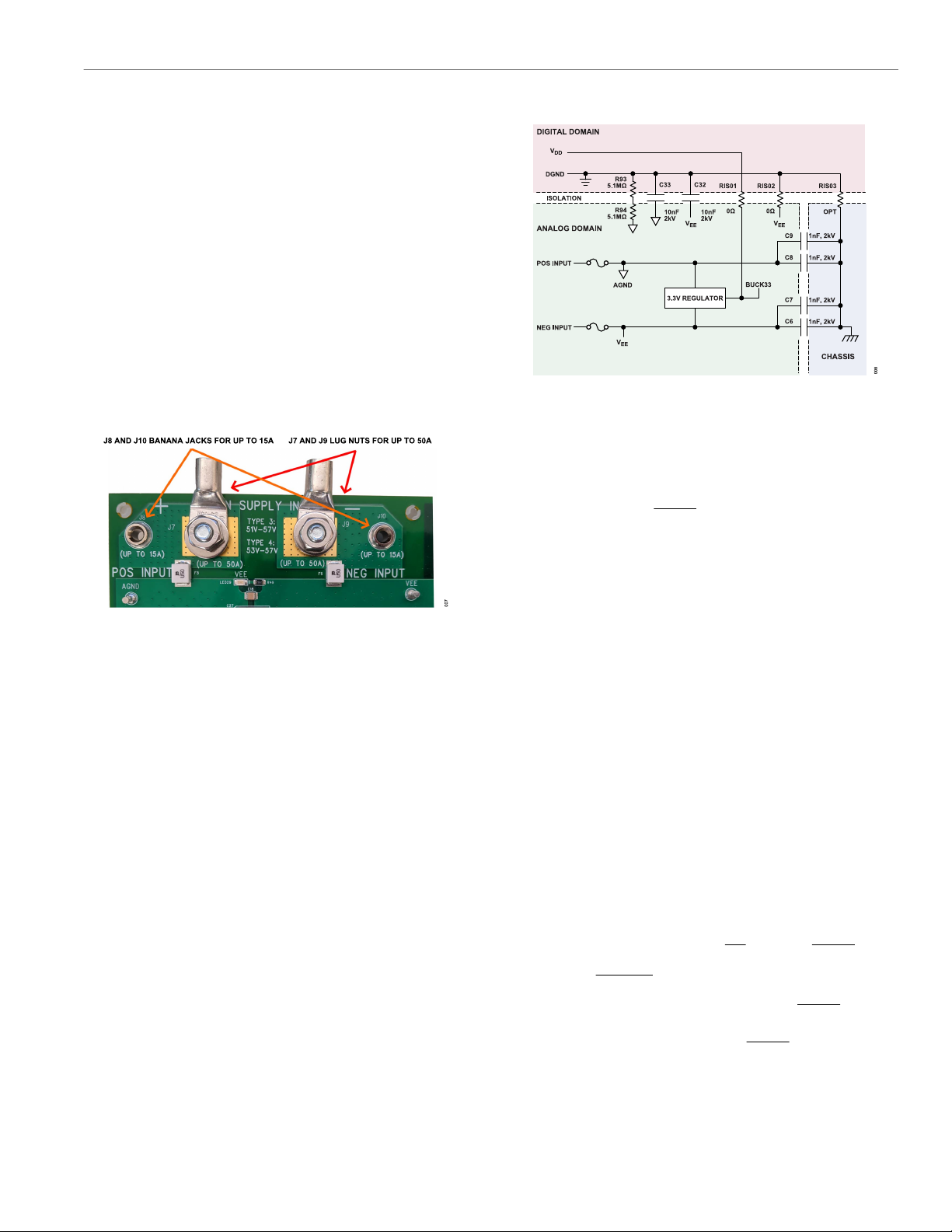
ISOLATION
The IEEE 802.3 Ethernet specifications require network segments
(including the analog PoE circuitry) to be electrically isolated from
the chassis ground. The DC3017A motherboard and DC3159A
daughter card layouts and high voltage capacitors provide an
isolation barrier between Analog and Digital domains. Transform-
ers provide a galvanic barrier between DGND and AGND on the
DC3159A daughter card. By default, this isolation barrier is bridged
by resistors on the motherboard to allow for evaluation using a
single power supply. Remove RISO1 and RISO2, then provide an
external 3.3 V supply between VDD and DGND to evaluate this
board as an isolated system.
All RJ45 shields and terminations are connected to chassis ground.
AGND and VEE each connect to chassis ground with two pairs of
1 nF, 2 kV capacitors (C6-C9). AGND and VEE also connect to
DGND each with 10 nF, 2 kV capacitors (C32-C33). An optional 0
Ω resistor can be installed at RISO3 to tie the chassis ground to
DGND. Two series 1206, 5.1 MΩ resistors connect between AGND
and DGND for high voltage capacitance discharge. See Figure 8
for connections between Analog and Digital domains, as well as
chassis ground on the DC3017A motherboard.
The DC3159A daughter card is laid out with isolation.
Figure 8. Motherboard Power Supply Connections and Isolation Barriers
PWRMD SETTINGS
The LTC9101-2/LTC9102 operating mode and maximum class
while in auto mode depends on the PWRMD0 pin state of the
LTC9102 at bus address ID:00b during reset. Reset occurs on a
VDD or VEE power cycle, RESET pin is pulled low and released
high, or when the global Reset All bit is set. Changing the state
of this pin will not change the PSE configuration until a reset
occurs. The PWRMD0 pin connects to the RPWRMD resistor using
the PWRMD-1 jumper. RPWRMD is used to automatically determine
the power allocation per port. See Table 2 for the PWRMD0 and
RPWRMD settings. The LTC9101-2A does not check the PWRMD0
pin state.
DEVICE CONFIGURATION
The CFG0 and CFG1 pins configure the number of analog control-
lers in the system. Each pin connects to a jumper that pulls either
HI for a logical 1, or LO for logical 0. CFG1 and CFG0 set the
number of analog controllers in the system. See Table 3 for the
CFG[1:0] settings.
DIGITAL CONNECTIONS
The DC590 USB to I2C controller board is connected to the
DC3017A-B motherboard at J1 through a 14-pin ribbon cable. The
LTC9101-2A or LTC9101-2 I2C address is set by the pins AD4,
AD3, AD2, and AD1. See I2C Address section for more information.
SDAOUT and SDAIN can be tied together through a shunt resistor,
R73. Turrets on the DC3017A-B motherboard provide test points for
SCL, SDAIN, SDAOUT, VDD, DGND, INT, OSS, and RESET.
OSS AND RESET PUSH BUTTONS
Push button switch SW1, when pressed, pulls the RESET pin of the
daughter card logic low. The PSE controller is then held inactive
with all ports off. When SW1 is released, RESET is pulled high, and
the PSE returns to the reset state.
Push button switch SW2, when pressed pulls the overload supply
shutdown input, OSS pin of the daughter card logic low. When