UG-340 8-/10-Lead PulSAR User Guide
EVALUATION BOARD HARDWARE
SETTING UP THE EVALUATION BOARD
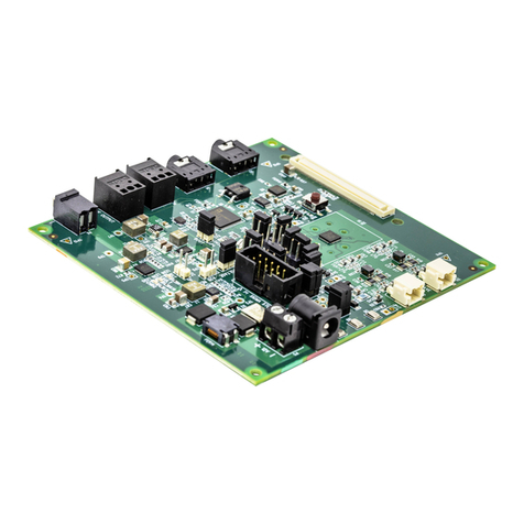
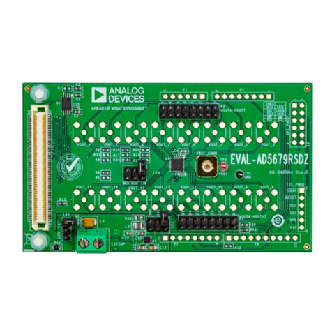
Figure 27 shows the evaluation board schematic. The board
consists of the ADC, U1, with a reference, U6 (ADR435), and
ADC drivers, U12 and U14 (ADA4841-1). The 8-lead board
also has a level shifter, U16 (ADG3304).
The evaluation board is a flexible design that enables the user to
adjust compensation components in addition to operating from
an adjustable bench top power supply.
POWER SUPPLIES
The evaluation board requires power from a wall adapter. The
on-board power supply design is designed to operate from 9 V.
Table 1. Power Supplies Provided on the Board
Power Supply (V) Function Components Used
+5 SDP power ADP2301
+7.5 Positive rail ADP7102
−2.5 Negative rail ADP2301
+2.5/+5 ADC ADP7104
+3.3 VDRIVE (digital power) ADP7104
Each supply is decoupled where it enters the board and again at
each device. A single ground plane is used on this board to
minimize the effect of high frequency noise interference.
In addition to this, there is also the ability to power the board
from a bench top power supply. The screw terminals, J2 and J3, are
provided for this function. When bench power is used, the wall
wart and on-board power supply are no longer required. Solder
links also must be changed: SL1 = B, SL2 = B, SL7 = B, SL4 = B,
and SL3 = B.
REFERENCE
An external 5 V reference (U6, ADR435) is used to supply the
ADCs directly.
SERIAL INTERFACE
The evaluation board uses the SPORT interface from the ADSP-
BF527 D S P.
A number of AND gates are used to clock and gate the SPORT
transfer to the ADC device. See U9, U10, and U11. The 8-lead
board also has a level shifter, U16 (ADG3304), which interfaces
the ADC logic levels (5 V) to the E VA L -SDP-CB1Z (3.3 V).
SOLDER LINKS
There is one three solder link option on the board. It is configured
depending on which generic of the ADC is on the specific
evaluation board as described in Table 3.
Table 2. Table of Jumper Detail with Factory Default Setting
Link Setting Function Comment
SL2 A −VSChange to B if using bench supplies
SL1 A +VSChange to B if using bench supplies
SL3 A V_SDP Change to B if using bench supplies
SL7 A VDD for
ADC
Change to B if using bench supplies
Change to B if using bench supplies
Table 3. Table of Jumpers Specific to Different ADCs
Link Setting Configuration Generic
SL10 A Differential
input
AD7684, AD7687, AD7688,
AD7690, AD7691, AD7693,
AD7982, AD7984, AD7989-5,
AD7915, AD7916
SL10 B Single-ended AD7683, AD7685, AD7686,
AD7694, AD7942, AD7946,
AD7980, AD7983, AD7988-5
ANALOG INPUTS
The analog inputs to the evaluation board are SMA connectors,
J6 and J10. These inputs are buffered with dedicated amplifier
circuitry (U12 and U14), as shown in Figure 27. The circuit allows
different configurations, input range scaling, filtering, addition of a
dc component, and use of different op amp and supplies. The
analog input amplifiers are set as unity-gain buffers at the factory.
The amplifier positive rail is driven from 7.5 V (from U13,
ADP7102). The negative amplifier rail is driven from –VS
(generated by U3, ADP2301).
The default configuration sets both U12 and U14 at midscale,
generated from a buffered reference voltage divider (VCM).
The evaluation board is factory configured for providing either
a single-ended path or a fully differential path as shown in Table 3.
For dynamic performance, a fast Fourier transform (FFT) test
can be done by applying a very low distortion ac source.
For low frequency testing, the audio precision source can be used
directly because the outputs on these are isolated. Set the outputs
for balanced and floating ground. Different sources can be used;
however, most are single-ended sources that use a fixed output
resistance.
Because the evaluation board uses the amplifiers in unity-gain,
the noninverting input has a common-mode input with a series
590 Ω resistor, and it needs to be taken into account when directly
connecting a source (voltage divider).
Rev. C | Page 4 of 31


