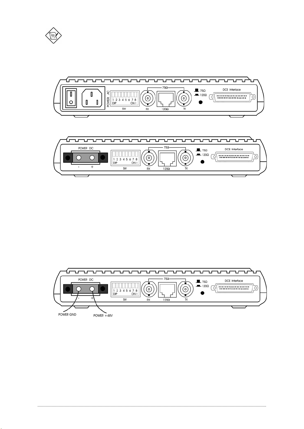
Anda Telecom FE1/V.35 User manual

FE1/V.35 Interface Converter
Version: V3.2.4
Date: 5.12.2005

User Manual
2-20
C
Co
on
nt
te
en
nt
ts
s
Chapter 1 Introduction..........................................................................3
1.1 Description................................................................................................ 3
1.2 Characteristics ........................................................................................... 3
1.3 Technical Parameters ................................................................................. 3
Chapter 2 Operation .............................................................................5
2.1 Front Panel ................................................................................................ 5
2.1.1 Indicators........................................................................................... 5
2.2 Back Panel................................................................................................. 6
2.2.1 Power Supply .................................................................................... 6
2.2.2 E1 Interface........................................................................................ 7
2.2.3 V.35 Interface .................................................................................... 7
2.2.4 Time Slots Settings ............................................................................. 9
2.2.5 Settings of SW.................................................................................. 11
Chapter 3 Installation..........................................................................15
3.1 Appearance checking............................................................................... 15
3.2 Installation process................................................................................... 15
3.3 Installation notice proceeding................................................................... 15
Chapter 4 Troubleshooting ..................................................................17
Chapter 5 Appendix Table...................................................................19

User Manual
3-20
Chapter 1 Introduction
1.1 Description
FE1/V.35 interface converter is designed based on an ASIC chip. The chip
adopts special patent technology of reduced dithering, digital phase
locked and distill clock, E1 anti-jamming, etc. The inner software and
hardware are all modularity, integrating coding, decoding, message
insertion and alarm, and make the circuit simple so as to improve the
reliability of the device. FE1/V.35 interface converter convert V.35 to E1,
and V.35 interface works at DCE mode.
1.2 Characteristics
yDithering tolerance and dithering transmission characteristic of E1
channel have high performance, which is superior to industry
standard
ySupport CAS and CCS mode
ySupport CRC-4 verifying
yFollow remote device settings can be set
yData rate of E1 interface N×64kbps(N=1~32)is adjustable
ySupport autosense V.35 phase
yThree clock modes are selectable
yThe circuit is designed simply, the device works steadily
1.3 Technical Parameters
Mode: DCE
Standard: comply with ITU-T V.35 standard
Data rate: N×64Kbps(N=1~32),framed
V.35
Interface
Connector: DB25 female
Data rate: N×64Kbps(N=1~32)
Tolerance: ±50ppm
Line code: HDB3
E1
Interface
Electric characteristic: comply with ITU-T G.703
standard

User Manual
4-20
Dithering characteristic: comply with ITU-T G.823
standard
Dithering tolerance: comply with ITU-T G.823 standard
Impedance: 75Ωunbalanced/ 120Ωbalanced
Clock mode
Internal clock (default)
External clock
Line clock
Voltage: AC110V/AC 240V/DC –48V/DC –48V/DC
+24V
Power
supply Power consumption: ≤5W
Environment
Working temperature: 0°C~50°C
Storage temperature: -40°C~+70°C
Relative humidity: 5%~95 %
Weight 0.4Kg
Size 212mm×150mm×38mm

User Manual
5-20
Chapter 2 Operation
2.1 Front Panel
Fig 1. Front panel of FE1/V.35 Interface Converter
2.1.1 Indicators
There are seven indicators in the front panel of FE1/V.35 interface converter,
from right to left:
yPWR Green Indicator of power supply
Bright when power is on
yE1LOS Red
Alarm indicator of E1 code-breaking
Bright when local device E1 code-breaking
Blinking when remote device E1 code-breaking
Local has higher priority
yE1LOF Red
Alarm indicator of E1 frame-lost
Bright when local device E1 frame lost
Blinking when remote device E1 frame lost.
Local has higher priority
yTXD Green Indicator of V.35 data transmittal
Blinking when V.35 data transmitted
yRXD Green Indicator of V.35 data receiving
Blinking when V.35 data received
yPTOK Green
Indicator of test result
OFF when device work normally
Bright when the test result is right
yTEST/
CRC_ERR
Double
colors
Indicator of test and CRC error
OFF when device work normally
Red: bright when local CRC error
Blinking when remote CRC error
Green: bright when device in test mode
Blinking when remote device in test mode
Table 1. Specification of front panel indicators

User Manual
6-20
NOTE:
External clock and the connected DTE device doses not supply clock,
E1LOS still bright when E1 looping.
2.2 Back Panel
Fig 2. Back panel of FE1/V.35 Interface Converter (AC)
Fig 3. Back panel of FE1/ V.35 Interface Converter (DC)
2.2.1 Power Supply
AC socket: AC 220V input.
DC socket:
If the power supply is +48V, connect the device + pole with power +48V
pole, the device – pole with power GND. +24V power supply must be
used with DC+24V model device:
Fig 4. Sketch map of DC+48V connection
If the power supply is -48V, connect the device + pole with power GND
pole, the device – pole with power -48V:

User Manual
7-20
Fig 5. Sketch map of DC-48V connection
NOTE:
Please check the power polarity carefully, and connect after everything is
confirmed. Otherwise the equipment may be caused the forever damages
and we won’t take any responsibility because of this!
2.2.2 E1 Interface
E1 75Ω/120Ωswitch
STATE 75 /120 INTERFACEΩΩ
120Ωbalanced interface
75 unΩbalanced interface
Table 2. Definition of E1 75 /120 switchΩΩ
75Ωunbalanced E1 interface connector are BNC connector, RX indicate
E1 input, TX indicate E1 output;
120Ωbalanced E1 interface connector is RJ45 connector, the pin
assignment defined as below:
Fig 6. Sketch map of RJ45 connector
120Ωbalanced E1 interface pin assignment:
PIN 1 2 3 4 5 6 7 8
Definition TxD+ TxD- RxD+ RxD-
Table 3. Pin assignment of 120Ωbalanced E1 interface
2.2.3 V.35 Interface
The DB25 Female connector in the rear panel is V.35 data interface:

User Manual
8-20
DB25 Pin No. Signal Function corresponding
1 Protective Ground A
7 Signal Ground B
2 Transmitted data A P
14 Transmitted data B S
3 Received data A R
16 Received data B T
4 Request to send C
5 Clear to send D
6 DCE ready E
20 DTE ready H
8 Data carrier wave tested F
24 Transmit clock A(from DTE) U
10 Transmit clock B(from DTE) W
15 Transmit clock A(from DCE) Y
12 Transmit clock B(from DCE) AA
17 Receive clock A(from DCE) V
9 Receive clock B(from DCE) X
Table4. V.35 Interface Signal Assignments
Connect FE1/V.35 Interface Converter with DTE device by the equipped
DB25M/M34F cable.
NOTE:
Connect with DCE device by intercross cable, facture of intercross cable
defined as below, note that some DCE device pin assignment are different:
A B
DB25 Pin Definition DB25 Pin Definition
1 Protective Ground 1 Protective Ground
7 Signal Ground 7 Signal Ground
2 Transmitted data A 3 Received data A
14 Transmitted data B 16 Received data B
3 Received data A 2 Transmitted data A
16 Received data B 14 Transmitted data B
4 Request to send 8 Data carrier wave tested
5 Clear to send 8 Data carrier wave tested
6 DCE ready 20 DTE ready
20 DTE ready 6 DCE ready
8 Data carrier wave tested 4 Clear to send
24 Transmit clock A(from DTE) 17 Receive clock A(from DCE)
11 Transmit clock B(from DTE) 9 Receive clock B(from DCE)
15 Transmit clock A(from DCE) /

User Manual
9-20
12 Transmit clock B(from DCE) /
17 Receive clock A(from DCE) 24 Transmit clock A(from DTE)
9 Receive clock B(from DCE) 11 Transmit clock B(from DCE)
Table 5. Facture of V.35 intercross cable
2.2.4 Time Slots Settings
Time slot settings switch for FE1/V.35 Interface Converter is located at the
bottom of the device. On the bottom board of FE1/ V.35 Interface
Converter, there is a quadrate slot. Under the slot, there are four 8-bit Dips
(totally 32 bits) for setting E1 time slots. From left to right NO.0~NO.31 bit
corresponding E1 TS0~TS31, ON when opening up the corresponding
time slot, OFF when closed.
Fig 7. Bottom panel of FE1/V.35 Interface Converter
Settings of time slot defined as below table (see the Chapter 5 Appendix
Table in detail):
SW Status Function Status Function Default
ON Unframed 2048KBps / /
0 OFF OFF OFF
16 ON
CCS (PCM31) OFF CAS (PCM30) ON
1 ON TS1 is available OFF TS1 is invalid ON
2 ON TS2 is available OFF TS2 is invalid ON
3 ON TS3 is available OFF TS3 is invalid ON
4 ON TS4 is available OFF TS4 is invalid ON
5 ON TS5 is available OFF TS5 is invalid ON
6 ON TS6 is available OFF TS6 is invalid ON
7 ON TS7 is available OFF TS7 is invalid ON
8 ON TS8 is available OFF TS8 is invalid ON

User Manual
10-20
9 ON TS9 is available OFF TS9 is invalid ON
10 ON TS10 is available OFF TS10 is invalid ON
11 ON TS11 is available OFF TS11 is invalid ON
12 ON TS12 is available OFF TS12 is invalid ON
13 ON TS13 is available OFF TS13 is invalid ON
14 ON TS14 is available OFF TS14 is invalid ON
15 ON TS15 is available OFF TS15 is invalid ON
16 ON TS16 is available OFF TS16 is invalid ON
17 ON TS17 is available OFF TS17 is invalid ON
18 ON TS18 is available OFF TS18 is invalid ON
19 ON TS19 is available OFF TS19 is invalid ON
20 ON TS20 is available OFF TS20 is invalid ON
21 ON TS21 is available OFF TS21 is invalid ON
22 ON TS22 is available OFF TS22 is invalid ON
23 ON TS23 is available OFF TS23 is invalid ON
24 ON TS24 is available OFF TS24 is invalid ON
25 ON TS25 is available OFF TS25 is invalid ON
26 ON TS26 is available OFF TS26 is invalid ON
27 ON TS27 is available OFF TS27 is invalid ON
28 ON TS28 is available OFF TS28 is invalid ON
29 ON TS29 is available OFF TS29 is invalid ON
30 ON TS30 is available OFF TS30 is invalid ON
31 ON TS31 is available OFF TS31 is invalid ON
Table 6. Settings of Time Slot
NOTE:
1) E1 framing status depends on NO.0 bit, OFF is framed, ON is
unframed.
2) E1 PCM30 or PCM31 depends on NO.16 bit, OFF is PCM30, TS16 is
used for transmitting singling; ON is PCM31, TS16 is used for
transmitting 64K data, if more than 64K, keep NO.16 bit ON and
open other bits.
3) All OFF is unframed, the rate is 2048KBps.
4) Default settings is that NO.0 bit is OFF, other bits are all ON.

User Manual
11-20
2.2.5 Settings of SW
ySummary
An 8-bit switch is located on the back panel, signed by “SW”, defined as
follows (from left to right):
SW CLOCK PHASE LOOP PATT FOLLOW
BIT 1 2 3 4 5 6 7 8
DEFAULT ON ON OFF OFF OFF OFF OFF ON
TITLE SW-1 SW-2 SW-3 SW-4 SW-5 SW-6 SW-7 SW-8
Table 7. Default settings of SW
yCLOCK Settings (SW-1, SW-2)
CLOCK SETTINGS
SW-1 (close the power) SW-2 Clock mode
ON ON INTERNAL clock (default)
OFF ON LINE clock (follow the opposite device
Time Slot settings)
OFF OFF EXTERNAL clock
Table 8. Clock settings
Internal clock (ON, ON): The clock generated by internal oscillator.
Line clock (OFF, ON): The clock recovered from receiving E1
signal, under this settings the device can
auto follow the opposite device Time slot
settings if the opposite device is INTERNAL
clock.
External clock (OFF,OFF): The clock obtains from V.35 port of
DTE/DCE device connected to.
NOTE:
1) Guarantee that there is only one Internal clock device in one chain.
2) Avoid that all device in one chain don’t set as Line clock. If it is
specific that Internal clock exist in chain, set the device Line clock. If
not, set the device as Internal clock.
3) When connected with DCE/DTE device and DCE/DTE device
generate clock, FE1/V.35 Interface Converter set as External clock.
yPhase setting(SW-3)
Bit 3 of SW in rear panel is used to set V.35 data phase. FE1/V.35 Interface
Converter can auto detect the phase of receiving data. The phase of
transmittal data can be set by this switch. Defied as below:

User Manual
12-20
SW Definition Specification Default
ON: sample when
rising
SW-3 Phase setting of transmittal V.35 data OFF: sample when
falling
OFF
Table 9. Phase setting of transmittal V.35 data
yLOOP Setting (SW-4, SW-5, SW-6)
BIT4, BIT5, BIT6 of SW (SW-4, SW-5, SW-6) are LOOP Setting, REM only
can used in framed E1, defined as below:
SW DEFINITION SPECIFICATION DEFAULT
ON: Loop
SW-4
Loop local
data back
ANA OFF: Work normally
OFF
ON: Loop
SW-5
Loop line
back
DIG OFF: Work normally
OFF
ON: Loop
SW-6
Loop the
remote device
REM OFF: Work normally
OFF
Table 10. Loop settings
SW-4: Loop local data back, shown as Fig 8:
Fig 8. Loop local data back
SW-5: Loop line back, shown as Fig 9:
Fig 9. Loop line back

User Manual
13-20
SW-6: Loop the remote device, use only in framed E1. shown as Fig 10:
Fig 10. Loop the remote device
yPATT (SW-7)
BIT7 of SW is PATT test, cooperate with loop settings to check up the
device and line. The result can get by observing PTOK:
LOCAL (Internal clock) REMOTE (Line clock) LOCAL
SW-4
ANA
SW-5
DIG
SW-6
REM
SW-7
PATT
SW-4
ANA
SW-5
DIG
SW-6
REM
SW-7
PATT PTOK TEST
CRC_ERR
SPECIFICATION
OFF OFF OFF OFF OFF OFF OFF OFF Not
bright
Not
bright Work normally
ON OFF OFF OFF OFF OFF OFF OFF Not
bright Green Loop local data
back
OFF ON OFF OFF OFF OFF OFF OFF Not
bright Green
Loop line back, if
E1 is framing, the
led of test in the
remote device is
blinking.
OFF OFF ON OFF OFF OFF OFF OFF Not
bright
Blinking
Green
Loop the remote
device, the led of
test in the remote
device is bright.
(This test is
effective in frame
E1.)
ON OFF OFF ON OFF OFF OFF OFF Bright Green Local device test
OK.
OFF OFF OFF ON OFF ON OFF OFF Bright Green Local device and
E1 line test OK.
OFF ON OFF ON OFF OFF OFF OFF Not
bright Green
Local device in test
mode and loop is
not set right. It is
inanition.
OFF OFF ON ON OFF OFF OFF OFF Bright Green
Local device,
remote device and
E1 line test OK.
This test is effective
in frame E1.
Table 11. PATT testing
NOTE:
After test resume all the test and loop switches to the default settings, all
OFF, or the device can’t work.

User Manual
14-20
yFollow(SW-8)
BIT8 of SW is used to set follow or unfollow the opposite device time slot
settings. Only used in LINE clock and the opposite device INTERNAL
clock:
SW Definition Specification Default
ON: unfollow
SW-8 Follow
OFF: follow ON
Table 12. Settings of follow
NOTE:
This function is available between the same type products (include Card
type) of our company.

User Manual
15-20
Chapter 3 Installation
3.1 Appearance checking
1) After you received the devices, firstly you should check whether the
packing is well, otherwise, please contact with our company or the
local agent in time so as to solve the problem.
2) After opening the box, you should check whether the device and the
fittings are correct and well according to the incasement list,
otherwise please contact with our company or the local agent.
3.2 Installation process
1) Firstly place the device at a steady position, the working environment
should be dry, tidy, ventilative, and the temperature should be
reasonable.
2) Check whether the clock and time slots control switch are right
before connecting the power supply. The device is set internal
oscillator when leave factory, if it is point-to-point application, please
adjust one side internal oscillator, the other side line clock, which
will follow the time slots setting automatically.
3) Check the power collocation of FE1/V.35 interface converter, if it is
DC model, please pay attention to the voltage value and polarity,
then connect the power supply referring to this manual.
4) Please test the device before using: open the power switch, indicator
(PWR) is bright, which show the power supply is normal; when you
don’t connect anything, PWR(Green)、E1LOS(Red) are all bright, the
others are off.
5) Shut down the power, connect the E1 cables and V.35 cables, set the
clock and time slots control switch correctly referring to this manual,
then open the power switch, the device will turn into normal working
state.
3.3 Installation notice proceeding
1) During the process of transportation and installation, the device
should be protected against vibration and mechanical damages.
2) Please examine the voltage value and whether the polarity is in
accord with the mark on the rear panel before electrifying, or else the

User Manual
16-20
device may be caused permanent damages.
3) The device has already adjusted optimal status before leaving factory,
please don’t take apart the device privately if non technicians of our
company.
4) When the device has failure, you can make sure the failure range
through self-loop function with the device, and contract with
technical service center of our company in time.

User Manual
17-20
Chapter 4 Troubleshooting
Normal working status: when FE1/V.35 interface converter works
normally, PWR (Green) indicator is bright, TXD (Yellow)、RXD (Yellow)
indicators are blinking, the others are off.
When the device has failure, firstly make sure the failure range
according to the status of the indicators, then deal with the problem.
yTrouble phenomenon: no reaction after electrifying
Diagnosis:
Examine the power supply, if it is DC model, make sure the
polarity, if the wire is connected inversely, please correct it! If it is
AC model, please make sure whether the power control switch is
open.
Exclusion:
Correct the power connection or open the power control switch.
yTrouble phenomenon: E1LOS indicator is bright
Diagnosis:
The device is set Internal oscillator, loopback the input and
output ports by E1 cable, if this indicator is off, then mainly
examine the E1 cable.
Exclusion:
Examine whether the receiving and transmitting E1 cables are
inverse, if so please correct them; whether the E1 connectors are
loosened, if so please make them again.
yTrouble phenomenon: E1LOS indicator is off, but E1LOF indicator
is bright
Diagnosis:
This trouble is about due to three reasons hereinafter:
1) The core doesn’t connect with skin of E1 input cable, or core
and skin are intercrossed, or only connect one thread of
120Ωcable.
2) The two sides are both set to internal clock, moreover the
time slots are different. Or one end is set to Internal clock,
the other end is set to line clock but isn’t set to follow the
time slots of the opposite end automatically, or the time slots
is wrong.
3) The FE1/V.35 interface converter works at external clock
mode, but the clock rate provided by the external device is
different from that of it.

User Manual
18-20
Exclusion:
1) Make the E1 cables again.
2) Make sure there is only one internal clock in the whole lines,
the others are all line clock. Adjust the time slots settings to
ensure that the device works at one kind of time slots
settings, or follow the time slots of the opposite device
automatically.
3) Adjust the clock rate of FE1/V.35 interface converter or the
device connected to it, ensure that the two devices both
work at the same kind of clock rate.
yTrouble phenomenon: some data has lost during the course of
communication
Diagnosis:
Make sure whether all devices are set to line clock or more than
Two are set to internal clock.
Exclusion:
Two internal clocks will lead to some data lost, two line clocks
may lead to the line not on-hook; adjust the clock to make sure
only one device provide clock in one line.
yTrouble phenomenon: the line can not get through when the device
connect to DCE devices
Diagnosis:
1) Please pay attention to the clock association when FE1/V.35
interface converter connect to DCE device via crossover
cable, if DCE device is set to internal clock, then FE1/V.35
interface converter should be set to external clock; if DCE
device is set to external clock, then FE1/V.35 interface
converter should be set to internal clock.
2) Confirm the line sequence of DCE device connected to
FE1/V.35 interface converter.
Exclusion:
1) Adjust the clock settings.
2) Make the V.35 crossover cable again according to the V.35
sequence provided in this manual.

User Manual
19-20
Chapter 5 Appendix Table
(PCM31)
1920K (PCM31)
1856K (PCM31)
1792K (PCM31)
1728K (PCM31)
1664K (PCM31)
1600K (PCM31)
1536K (PCM31)
1472K (PCM31)
1408K (PCM31)
1344K (PCM31)
1280K (PCM31)
1216K (PCM31)
1152K (PCM31)
1088K (PCM31)
1024K (PCM31)
960K (PCM31)
896K (PCM31)
832K (PCM31)
768K (PCM31)
704K (PCM31)
640K (PCM31)
576K (PCM31)
512K (PCM31)
448K (PCM31)
384K (PCM31)
320K (PCM31)
256K (PCM31)
192K (PCM31)
128K (PCM31)
64K (PCM31)
Rate SW
OFF
OFF
OFF
OFF
OFF
OFF
OFF
OFF
OFF
OFF
OFF
OFF
OFF
OFF
OFF
OFF
OFF
OFF
OFF
OFF
OFF
OFF
OFF
OFF
OFF
OFF
OFF
OFF
OFF
OFF
OFF
0
ON
ON
ON
ON
ON
ON
ON
ON
ON
ON
ON
ON
ON
ON
ON
ON
ON
ON
ON
ON
ON
ON
ON
ON
ON
ON
ON
ON
ON
ON
1
ON
ON
ON
ON
ON
ON
ON
ON
ON
ON
ON
ON
ON
ON
ON
ON
ON
ON
ON
ON
ON
ON
ON
ON
ON
ON
ON
ON
ON
2
ON
ON
ON
ON
ON
ON
ON
ON
ON
ON
ON
ON
ON
ON
ON
ON
ON
ON
ON
ON
ON
ON
ON
ON
ON
ON
ON
ON
3
ON
ON
ON
ON
ON
ON
ON
ON
ON
ON
ON
ON
ON
ON
ON
ON
ON
ON
ON
ON
ON
ON
ON
ON
ON
ON
ON
4
ON
ON
ON
ON
ON
ON
ON
ON
ON
ON
ON
ON
ON
ON
ON
ON
ON
ON
ON
ON
ON
ON
ON
ON
ON
ON
5
ON
ON
ON
ON
ON
ON
ON
ON
ON
ON
ON
ON
ON
ON
ON
ON
ON
ON
ON
ON
ON
ON
ON
ON
ON
6
ON
ON
ON
ON
ON
ON
ON
ON
ON
ON
ON
ON
ON
ON
ON
ON
ON
ON
ON
ON
ON
ON
ON
ON
7
ON
ON
ON
ON
ON
ON
ON
ON
ON
ON
ON
ON
ON
ON
ON
ON
ON
ON
ON
ON
ON
ON
ON
8
ON
ON
ON
ON
ON
ON
ON
ON
ON
ON
ON
ON
ON
ON
ON
ON
ON
ON
ON
ON
ON
ON
9
ON
ON
ON
ON
ON
ON
ON
ON
ON
ON
ON
ON
ON
ON
ON
ON
ON
ON
ON
ON
ON
10
ON
ON
ON
ON
ON
ON
ON
ON
ON
ON
ON
ON
ON
ON
ON
ON
ON
ON
ON
ON
11
ON
ON
ON
ON
ON
ON
ON
ON
ON
ON
ON
ON
ON
ON
ON
ON
ON
ON
ON
12
ON
ON
ON
ON
ON
ON
ON
ON
ON
ON
ON
ON
ON
ON
ON
ON
ON
ON
13
ON
ON
ON
ON
ON
ON
ON
ON
ON
ON
ON
ON
ON
ON
ON
ON
ON
14
ON
ON
ON
ON
ON
ON
ON
ON
ON
ON
ON
ON
ON
ON
ON
ON
15
ON
ON
ON
ON
ON
ON
ON
ON
ON
ON
ON
ON
ON
ON
ON
ON
ON
ON
ON
ON
ON
ON
ON
ON
ON
ON
ON
ON
ON
ON
ON
16
ON
ON
ON
ON
ON
ON
ON
ON
ON
ON
ON
ON
ON
ON
ON
17
ON
ON
ON
ON
ON
ON
ON
ON
ON
ON
ON
ON
ON
ON
18
ON
ON
ON
ON
ON
ON
ON
ON
ON
ON
ON
ON
ON
19
ON
ON
ON
ON
ON
ON
ON
ON
ON
ON
ON
ON
20
ON
ON
ON
ON
ON
ON
ON
ON
ON
ON
ON
21
ON
ON
ON
ON
ON
ON
ON
ON
ON
ON
22
ON
ON
ON
ON
ON
ON
ON
ON
ON
23
ON
ON
ON
ON
ON
ON
ON
ON
24
ON
ON
ON
ON
ON
ON
ON
25
ON
ON
ON
ON
ON
ON
26
ON
ON
ON
ON
ON
PCM31
27
ON
ON
ON
ON
Blank is OFF!
28
ON
ON
ON
29
ON
ON
30
ON
31
Reference Table of Time Slot Settings
——
PCM31

User Manual
20-20
2048K
2048K
1920K (PCM30)
1856K (PCM30)
1792K (PCM30)
1728K (PCM30)
1664K (PCM30)
1600K (PCM30)
1536K (PCM30)
1472K (PCM30)
1408K (PCM30)
1344K (PCM30)
1280K (PCM30)
1216K (PCM30)
1152K (PCM30)
1088K (PCM30)
1024K (PCM30)
960K (PCM30)
896K (PCM30)
832K (PCM30)
768K (PCM30)
704K (PCM30)
640K (PCM30)
576K (PCM30)
512K (PCM30)
448K (PCM30)
384K (PCM30)
320K (PCM30)
256K (PCM30)
192K (PCM30)
128K (PCM30)
64K (PCM30)
Rate SW
ON
OFF
OFF
OFF
OFF
OFF
OFF
OFF
OFF
OFF
OFF
OFF
OFF
OFF
OFF
OFF
OFF
OFF
OFF
OFF
OFF
OFF
OFF
OFF
OFF
OFF
OFF
OFF
OFF
OFF
OFF
0
ON
ON
ON
ON
ON
ON
ON
ON
ON
ON
ON
ON
ON
ON
ON
ON
ON
ON
ON
ON
ON
ON
ON
ON
ON
ON
ON
ON
ON
ON
1
ON
ON
ON
ON
ON
ON
ON
ON
ON
ON
ON
ON
ON
ON
ON
ON
ON
ON
ON
ON
ON
ON
ON
ON
ON
ON
ON
ON
ON
2
ON
ON
ON
ON
ON
ON
ON
ON
ON
ON
ON
ON
ON
ON
ON
ON
ON
ON
ON
ON
ON
ON
ON
ON
ON
ON
ON
ON
3
ON
ON
ON
ON
ON
ON
ON
ON
ON
ON
ON
ON
ON
ON
ON
ON
ON
ON
ON
ON
ON
ON
ON
ON
ON
ON
ON
4
ON
ON
ON
ON
ON
ON
ON
ON
ON
ON
ON
ON
ON
ON
ON
ON
ON
ON
ON
ON
ON
ON
ON
ON
ON
ON
5
ON
ON
ON
ON
ON
ON
ON
ON
ON
ON
ON
ON
ON
ON
ON
ON
ON
ON
ON
ON
ON
ON
ON
ON
ON
6
ON
ON
ON
ON
ON
ON
ON
ON
ON
ON
ON
ON
ON
ON
ON
ON
ON
ON
ON
ON
ON
ON
ON
ON
7
ON
ON
ON
ON
ON
ON
ON
ON
ON
ON
ON
ON
ON
ON
ON
ON
ON
ON
ON
ON
ON
ON
ON
8
ON
ON
ON
ON
ON
ON
ON
ON
ON
ON
ON
ON
ON
ON
ON
ON
ON
ON
ON
ON
ON
ON
9
ON
ON
ON
ON
ON
ON
ON
ON
ON
ON
ON
ON
ON
ON
ON
ON
ON
ON
ON
ON
ON
10
ON
ON
ON
ON
ON
ON
ON
ON
ON
ON
ON
ON
ON
ON
ON
ON
ON
ON
ON
ON
11
ON
ON
ON
ON
ON
ON
ON
ON
ON
ON
ON
ON
ON
ON
ON
ON
ON
ON
ON
12
ON
ON
ON
ON
ON
ON
ON
ON
ON
ON
ON
ON
ON
ON
ON
ON
ON
ON
13
ON
ON
ON
ON
ON
ON
ON
ON
ON
ON
ON
ON
ON
ON
ON
ON
ON
14
ON
ON
ON
ON
ON
ON
ON
ON
ON
ON
ON
ON
ON
ON
ON
ON
15
OFF
OFF
OFF
OFF
OFF
OFF
OFF
OFF
OFF
OFF
OFF
OFF
OFF
OFF
OFF
OFF
OFF
OFF
OFF
OFF
OFF
OFF
OFF
OFF
OFF
OFF
OFF
OFF
OFF
OFF
16
ON
ON
ON
ON
ON
ON
ON
ON
ON
ON
ON
ON
ON
ON
ON
17
ON
ON
ON
ON
ON
ON
ON
ON
ON
ON
ON
ON
ON
ON
18
ON
ON
ON
ON
ON
ON
ON
ON
ON
ON
ON
ON
ON
19
ON
ON
ON
ON
ON
ON
ON
ON
ON
ON
ON
ON
20
ON
ON
ON
ON
ON
ON
ON
ON
ON
ON
ON
21
ON
ON
ON
ON
ON
ON
ON
ON
ON
ON
22
ON
ON
ON
ON
ON
ON
ON
ON
ON
23
ON
ON
ON
ON
ON
ON
ON
ON
24
ON
ON
ON
ON
ON
ON
ON
25
ON
ON
ON
ON
ON
ON
26
ON
ON
ON
ON
ON
PCM30
27
ON
ON
ON
ON
Blank is OFF!
28
ON
ON
ON
29
ON
ON
30
ALLOFF
ANY Settings
ON
31
Reference Table of Time Slot Settings
——
PCM30
Table of contents
Popular Media Converter manuals by other brands

B+B SmartWorx
B+B SmartWorx 232OTTL quick start guide

METRObility Optical Systems
METRObility Optical Systems twister 2131-34-01 Installation & user guide

Raisecom
Raisecom RC952-FEE1-BL user manual

ADF Web
ADF Web HD67B21-B2 user manual

Pulsar
Pulsar DC/DC50HV manual

GRASS VALLEY
GRASS VALLEY 8935CF - datasheet