RoHS compliant
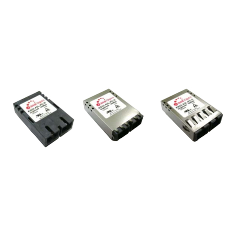
CWDM 1550 nm Single-mode Transceiver (24dB margin)
1×9, SC Duplex Connector, 3.3 V/5V
1.0625Gbd Fiber Channel/1.25 Gigabit Ethernet
Page 6 of 14
Version 1.1
Date:1/30/2006
Headquarters :
12 Shyr Jiann Road, Hsinchu Industrial Park, Hukow,
Hsinchu Hsien,, Taiwan 303
TEL: +886-3-5986799
FAX: +886-3-5986655
Website: www.apacoe.com.tw
Connection Diagram
Pin-Out
1. RX GND
2. RD+
3. RD
−
4. SD
5. VCCR
6. VCCT
7. TD
−
8. TD+
9. TX GND
TOP VIEW
N/C
N/C
PIN SYMBOL DESCRIPTION
1 RX GND Receiver Signal Ground.
Directly connect this pin to the receiver ground plane.
2 RD+RD+ is an open-emitter output circuit.
Terminate this high-speed differential LVPECL/PECL output with standard LVPECL/PECL techniques
at the follow-on device input pin. (See recommended circuit schematic)
3 RD−RD– is an open-emitter output circuit.
Terminate this high-speed differential LVPECL/PECL output with standard LVPECL/PECL techniques
at the follow-on device input pin. (See recommended circuit schematic)
4 SD
Signal Detect.
Normal optical input levels to the receiver result in a logic “1” output, VOH, asserted. Low input optical
levels to the receiver result in a fault condition indicated by a logic “0” output VOL, deasserted Signal
Detect is a single-ended LVPECL/PECL output. SD can be terminated with LVPECL/PECL techniques
via 50 Ωto VCCR
−
2 V. Alternatively, SD can be loaded with a 180 Ωresistor to RX GND to conserve
electrical power with small compromise to signal quality. If Signal Detect output is not used, leave it
open-circuited. This Signal Detect output can be used to drive a LVPECL/PECL input on an upstream
circuit, such as, Signal Detect input or Loss of Signal-bar.
5 VCCR Receiver Power Supply.
Provide +3.3 Vdc via the recommended receiver power supply filter circuit. Locate the power supply
filter circuit as close as possible to the VCCR pin.
6 VCCT Transmitter Power Supply.
Provide +3.3 Vdc via the recommended transmitter power supply filter circuit. Locate the power supply
filter circuit as close as possible to the VCCT pin.
7 TD−Transmitter Data In-Bar.
Terminate this high-speed differential LVPECL/PECL input with standard LVPECL/PECL techniques at
the transmitter input pin. (See recommended circuit schematic)
8 TD+Transmitter Data In.
Terminate this high-speed differential LVPECL/PECL input with standard LVPECL/PECL techniques at
the transmitter input pin. (See recommended circuit schematic)
9 TX GND Transmitter Signal Ground.
Directly connect this pin to the transmitter signal ground plane. Directly connect this pin to the
transmitter ground plane.


