Arcam T51 User manual

T51
DiVA T51
AM/FM Tuner
Service Manual
ARCAM
ARCAM
Issue 1.0

Contents List
!
Contents list
!
Circuit description
!
Circuit diagrams
!
Component overlays
!
Circuit board parts list
!
General assembly parts list

T51 Tuner Circuit Description
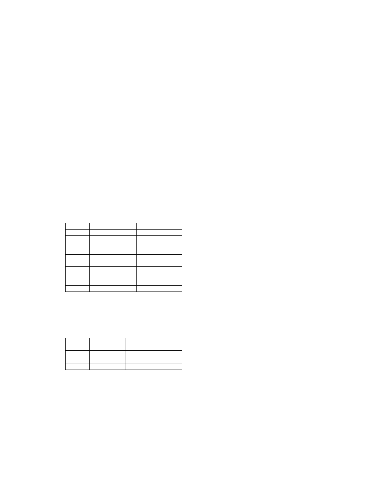
Power Supply
Mains voltage selection is made by placing a fuse, of
appropriate value, in the 115V or 230V position.
The single secondary is rectified and regulated and
supplies four regulators.
Z7 is always powered when the mains is connected and
keeps the preset memory of the micro controller intact.
The high-value capacitor (C84) will keep this data safe, for
a limited time, in case of mains power failure.
Z5 provides the main 12V supply rail for the RF and audio
circuits. This is always connected, except for the supply to
the FM front end, which is disabled by Q2 when the unit is
turned 'off'.
Z4 powers the LED back light on the display PCB.
Z6 is the 5V digital supply for the micro controller.
FM Tuner & IF
The FM aerial input is mixed in the front end FE1 which
provides a 10.7MHz IF output. This is filtered and
amplified by ceramic filters CF1 & CF2 and the circuit
based around Q9 & Q10. A third filter CF3 can be put in
circuit by fitting jumpers JP1 & JP2 across pins 2 & 4 and
1 & 3 of SK6 respectively. This effectively narrows the IF
band to improve selectivity. Transistors Q17 and Q21 are
part of the AGC circuit. The position of the jumper link
JP7 to either SK10 or SK11 determines from which point
the AGC circuit is triggered. The default is for the jumper
to be fitted to SK10 which minimizes cross modulation
and prevents the IF amp becoming saturated.
The LA1266 (Z9) demodulates the IF at pin 1 into an
audio output at pin 12. The quadrature coil is a
double-tuned device for best distortion performance.
When a station is tuned correctly the 'On Tune' signal goes
low and drives a green LED on the display PCB. This
signal is also used by the auto-stop detection and muting
circuits.
AM Tuner & IF
The LA1266 (Z9) contains the AM RF amplifier, oscillator
and mixer circuitry.
Switching between FM and AM modes is controlled by the
'FM' signal from the micro controller which disables the
AM circuitry of Z9 and switches the path of the audio
signal through Z8.
MW/LW switching is performed by switching transistors
Q12, Q14 & Q15.
Each band has its own oscillator and aerial tuning coils,
tuned by a varicap diode all contained within the AM
module L5.
The 450kHz IF signal is filtered by coil and ceramic filter
combination T5.
Birdie Filter
The ‘Birdie Filter’ (L2) is a four pole low pass filter, flat to
about 53kHz, then with a very steep roll off from then on..
This is designed to reduce co-channel interference in FM
Stereo and cut down on irritating ‘birdie’ noises.
Stereo Decoder
Stereo decoding is performed by LA3401 (Z8). The 38kHz
reference signal is accurately created by ceramic resonator
X3 and does not require adjustment.
Stereo separation is adjusted for maximum by preset RV1.
This IC also contains FM/AM audio switching and muting
functions.
Audio Filters & Output
The left and right channel audio outputs from Z8 are
filtered by the de-emphasis network of R1, C1 etc. The
correct de-emphasis network is selected by the position of
jumpers JP3 & JP4 on the pins of SK8. C2 & C102
(220pF) are selected for 50us and C3 & C103 (560pF) for
75us de-emphasis.
The final filter, based on Z3, is a two-pole low-pass circuit
with a cut-off frequency of around 20kHz. Also included
is a 19kHz notch filter, L1 & C4, that removes most of the
residual pilot tone.
Muting
When the power switch is turned off Q5 is switched off,
enabling the mute circuitry of the stereo decoder (Z8) via
diode D9. This removes the need for output muting
transistors and eliminates switching clicks and pops.
At switch-on the mute is enabled while C21 is charged via
Z8.
In normal use the mute inside Z8 is enabled in three other
ways:
The AMUTE signal from the micro controller is active at
power-on and for a short time when a preset is changed.
When the band is changed the output is muted by charging
C52.
The audio output must be muted whenever the tuner is in
stereo mode and is also off-tune. This is to eliminate noise
during tuning and is provided by Q8 and the MONO and
OFF TUNE control signals.
In Mono mode this mute is disabled so that weak stations
can be heard, despite the noise.
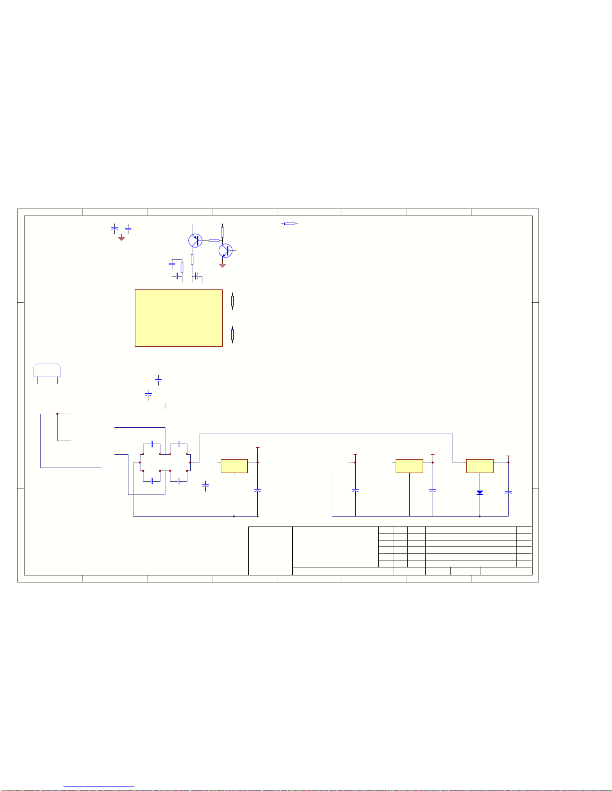
Micro controller
Control of the DiVA T51 tuner is performed by a single
micro controller Z10, LA7230. This also provides keypad
input and drives a LCD directly.
At power-on a matrix of diodes is scanned to set-up the
controller for the correct options:
D7 selects the correct frequency ranges.
D10 enables the use of Auto tuning as well as manual
tuning.
D8 allows the Auto-tuning mode to use the ‘IF Count’
method of searching.
The position of jumpers JP 5 & JP6 fitted to SK9 are used
to disable or enable LW and also whether the AM band
steps are 9 kHz (UK) or 10 kHz (USA).
Z10 provides control signal outputs for the following
functions:
MONO - To defeat the stereo decoder

AMUTE - Turns on the mute circuit when a button is
pressed & during tuning.
FM, MW & LW - Only one output active low at any one
time. Used to switch on specific parts of the RF circuitry as
appropriate.
The micro controller includes a Phase-Locked-Loop (PLL)
circuit which compares the tuner local oscillator signals
(FMIN & AMIN) with a reference frequency. Based on
this information and the required tuned frequency the
controller varies the tuning voltage to the FM and AM
front ends.
The tuning voltages (FMVt & AMVt) have to be filtered
from the PLL by the circuitry around Q7 & Q13.
Display PCB
The display PCB holds the keypad, LCD display, LED
back light module and On-Tune indicator.
The remote control receiver consists of the receiver RX1
and the PIC micro controller, Z1, which is used to decode
the incoming remote control codes from RC5 format to
Sanyo type commands. This is because the Sanyo micro
controller, Z10, can only respond to Sanyo remote control
commands.
Jumper Settings
Jumper Option 1 Option 2
JP1 Best sensitivity Best sound
JP2 Best sensitivity Best sound
JP3 De-emphasis 50uS De-emphasis
75uS
JP4 De-emphasis 50uS De-emphasis
75uS
JP5 LW & MW MW only
JP6 AM spacing 9KHz AM spacing
10KHz
JP7 Less X-MOD Less De-sense
USA / Rest of the World
If the T51 is transferred from or to the USA the
following jumper settings will require changing.
Jumper Rest of the
World USA Action
JP3 50uS 75uS De-emphasis
JP4 50uS 75uS De-emphasis
JP6 9KHz 10KHz AM spacing

12345678
A
B
C
D
87654321
D
C
B
A
ISSUE
DRAWING NO.
DRAWING TITLE
Drawn by:
DATE
Filename ECO No. DESCRIPTION OF CHANGE
G:\DATA\ECO\ECO AGENDA\00_1078 L892 T51 TUNER\L892_1\L892_1.ddb - L892c1_1_2.prj
A & R Cambridge Ltd.
Pembroke Avenue
Denny Industrial Centre
Waterbeach
Cambridge CB5 9PB
T51 Tuner
Circuit Diagram
L892CT
CL
12-Sep-2000
INITIALS
Date Printed 1 4Sheet of
Notes:
LK18
LK19
LK20
LK22
LK23
LK24
LK25
LK26
LK27
LK28
LK29
LK30
LK31
LK32
LK33
LK34
LK35
LK36
LK37
LK38
LK39
LK40
LK41
LK43
LK44
LK45
LK46
LK47
LK48
LK49
LK50
LK51
LK52
LK53
LK54
Tie
Cable
EL10
CABLE_TIE
F3
T100MASP
Kit Mask
Exclude 'NF' parts from kit mask, i.e. Not Fitted.
This applies to R4 and R104
PCB
PCB L892PB_1
Detail
Drilling
DD1
DRILL_DWG
Paper Marker
A2 Vertical
DD2
DD_A2V
Paper Marker
A2 Horizontal
DD3
DD_A2H
PD1
TOOLING
PD2
TOOLING
PD3
TOOLING
PD4
TOOLING
FIX1 FIX2 FIX3 FIX4FIX5
FIX6 FIX7 FIX8
Tooling & Fixing Holes
Tooling Holes Main PCB Fixing Holes
LCTR
HCTR
SD
AMIN
IFCNT
FM
LW
ON TUNE
FM Audio
AM Audio
FMVt
AMVt
OFF TUNE
Power Mute
LO
SCAN
FM/AM IF Demodulator
L892C2_1_2.SCH
FM Audio
AM Audio
FM
AMUTEOFF TUNE
MONO
STEREO
Power Mute
PICMUTE
Stereo decoder and Audio
L892C3_1_2.SCH
AMIN
FMVt
AMVt
HCTR
LCTR
STEREO
FM
LW
MONO
IFCNT AMUTE
SD
ON TUNE
LO
MW
PICMUTE
SCAN
Microprocessor and PLL
L892C4_1_2.SCH
Photo Strip
PS
PHOTO_STRIP
CEM1, 2 OZ Cu
PCB MATERIAL
DD4
CEM1_20Z
Photo Block
PHOTO_BLOCK
LK55
LK56
LK57
1
LK58
LK59
LK60
Update Box
EL1
UPDATE_BOX
CL 17/7/00 PRODUCTION RELEASE00-1044
1.2
00_1078 CL 12/09/00 R93 WAS 220R NOW 1K0

12345678
A
B
C
D
87654321
D
C
B
A
ISSUE
DRAWING NO.
DRAWING TITLE
Drawn by:
DATE
Filename
ECO No. DESCRIPTION OF CHANGE
G:\DATA\ECO\ECO AGENDA\00_1078 L892 T51 TUNER\L892_1\L892_1.ddb - L892C2_1_2.SCH
A & R Cambridge Ltd.
Pembroke Avenue
Denny Industrial Centre
Waterbeach
Cambridge CB5 9PB
T51 Tuner
Circuit Diagram
L892CT
CAH/SJB
12-Sep-2000
INITIALS
Date Printed 2 4Sheet of
1
2
SK10
2WVERTJUMPER
CF3
SFE10.7MLA
FM I/P
1
2
3
GND
4
Quad 1
5
Quad 2
6
Vcc
7
On Tune
8
AFC
9
FM IF
10
AM IF
11
FM O/P
12 STRQ 13
14
AM O/P 15
S meter 16
AM adj 17
IF in 18
AGC 19
IF out 20
AM I/P 21
Reg 22
Osc 23
AM Osc 24
Z9
LA1266
CF1
SFE10.7MLA
R66
220R MF
C38
10N CD
R71
330R MF
Q9
BC549B
Q10
BC557B
C45 47N CD
C46
47N CD
C69 100P CD
C70 100P CD
R77
15K MF
R52
22R MF
R55
22K MF
R78
22K MF
+C10
100U EL
C14
10N CD
P12V
R46
10R FU
+
C22
10U EL
C47
47N CD
LCTR
HCTR
SD
AMIN C65 1N0 CD
+C23
10U EL
IFCNT
P12V
R47
10R FU
+
C24
10U EL
C30
10N CD
C48
47N CD
C49
47N CD
R16
22K MF C50
47N CD
R79
5K1 MF
+
C53
1U0 EL
+
C54
1U0 EL
R44
68K MF
Q3
BC557B
P12V
R37
4K7 MF
FM
LW
R38
4K7 MF
Q11
BC547B
Low = AM
ON TUNE
R80
1K0 MF
R17
10K MF +C55
1U0 EL
To 'On-Tune' LED on display
R75
1K2 MF
C86
100P PP
FM Audio
AM Audio
R69
18K MF
FMVt
FM
Gnd
AM
R87
4K7 MF
P12V
T5 AM_IFT
AMVt
A_FMRF
A_AMRF
A_FMGND
A_FMLO
A_AMLO
A_FMVT
A_AMVT
A_ONTUNE
A_FMAUD
A_AMAUD
A_SMETER
A_FMBIRD
A
F
OFF TUNE
R68
4K7 MF
P5V
Q19
BC557B
R92
4K7 MF
P5V
Q2
BC557B
Q6
BC547B
R10
10K MF
R25
10K MF Power Mute
R94
4K7 MF
C42
22P CD
TP7
TP6
!
!
LO
A_AMSIG1
A_AMSIG2
A_AMSIG3
R40
100K MF
R53
100K MF
R29
10K MF
R24
2K7 MF
R28
2K7 MF
R43
2K7 MF
1
2
3
4
5
6
7
8
Birdie Filter
L2
BIRDIE
IF Out 7
Gnd
4
LO Out 8
V Tune
5
Vcc 6
Gnd
3Gnd
2
Ant
1
Case
FE1
MITSUMI_FE
16
4
Can
3
2
L3
QUAD_COIL_A
43
1
Can
6
2
L4
QUAD_COIL_B
R56
5K6 MF
R58
100K MF
C85
10N CD
R19
6K8 MF
CF2
SFE10.7MLA
SK7
FMAMANT2
4A
1A
3A
6A
2A
1B
2B
3B4B
5A
6B
1C
2C
3C
13
2
1D
2D
3D 4D
5D
6D
4C
6C
8
89
95
56
64
47
7
Cans
L5
AM_MODULE
R20
10K MF
C66
680P PP
+
C31
10U EL
+
C25
10U EL
B
A_IFOUT
A_FMIN
A_LW
A_AMGND
R57
220R MF
C34
10P CD
Q15
BC547B
Q14
BC547B
Q12
BC547B
+
C26
1U0 EL
C39
100N PC
C27
100N PC
1 2
3 4
5 6
SK6 DIL6 VPLG
C67 47P CD
JP1
JUMPER
JP2
JUMPER
Link 1&3, 2&4 for best sound quality,
Link 3&5, 4&6 for best selectivity.
D24
1N4148
C28
10N CD
R15
390R MF
R51
10K MF
Q17
ZVNL120
D25
1N4148
D26
1N4148
C41 10N CD
R73 1M0 MF
C43 10N CD
R76
330R MF
R81
330R MF
C63
10N CD
Q21
J112
R83
1K0 MF
D27
1N4148
R72
1K2 MF
SCAN
Mount Close to L3
AGC
R84
47K MF
R85
3K3 MF
C71
1N3 PP
FMCENTRE
TP9
JP7
JUMPER
1
2
SK11
2WVERTJUMPER
Fit JP7 to SK10 for less cross-mod,
Fit JP7 to SK11 for less de-sensing.
1
+
C73
100U EL
R88
4K7 MF
C75
1N0 CD
C76
1N0 CD R89
10R MF
00_1044 MGM 31/7/00 INITIAL RELEASE
R70
68R MF
R67
820R MF
R93
1K0 MF
1.2
00_1078 CL 12/09/00 R93 WAS 220R NOW 1K0

12345678
A
B
C
D
87654321
D
C
B
A
ISSUE
DRAWING NO.
DRAWING TITLE
Drawn by:
DATE
Filename
ECO No. DESCRIPTION OF CHANGE
G:\DATA\ECO\ECO AGENDA\00_1078 L892 T51 TUNER\L892_1\L892_1.ddb - L892C3_1_2.SCH
A & R Cambridge Ltd.
Pembroke Avenue
Denny Industrial Centre
Waterbeach
Cambridge CB5 9PB
T51Tuner
Circuit Diagram
L892CT
CAH/SJB
12-Sep-2000
INITIALS
Date Printed 3 4Sheet of
R30
4K7 MF
R31
4K7 MF
R33
4K7 MF
R41
5K6 MF
C35
470N PE
C36
470N PE
+
C74
100U EL C29
10N CD
+
C51
1U0 EL
Q1
BC557B
Q4
BC547B
+
C16
10U EL
C56
1N0 PP
R1
91K MF
R101
91K MF
R45 10R FU
Vin
I
GND
G
Vout O
Z6 7805
Vin
I
GND
G
Vout O
Z5 7812
+
C58
3M3 EL +C72
100U EL +C20
100U EL +C18
100U EL
Vin
I
GND
G
Vout O
Z7
7805
D22
1N4003F +C68
100U EL
P5V P5V6
P12V
VBL
Audio &
RF
Power
Supply
Backlight
Power
Supply Digital
Power
Supply
Back-up
Power
Supply
C591N0 CD C601N0 CD
C611N0 CD C62 1N0 CD
NL
SK5 IEC2

12345678
A
B
C
D
87654321
D
C
B
A
ISSUE
DRAWING NO.
DRAWING TITLE
Drawn by:
DATE
Filename
ECO No. DESCRIPTION OF CHANGE
G:\DATA\ECO\ECO AGENDA\00_1078 L892 T51 TUNER\L892_1\L892_1.ddb - L892C4_1_2.SCH
A & R Cambridge Ltd.
Pembroke Avenue
Denny Industrial Centre
Waterbeach
Cambridge CB5 9PB
T51 Tuner
Circuit Diagram
L892CT
CAH/SJB
12-Sep-2000
INITIALS
Date Printed 4 4Sheet of
XIN
1
TEST 1
2
REMO
3
STEREO
4
K5
5
K4
6
VOL
7
FM
8
MW
9
LW
10
SW1/VU
11
SW2/VD
12
MO/ST
13
MUTE
14
CE
15
DO
16
CLK
17
IFCNT
18
NARROW
19
PWROUT
20
AMUTE
21
STB
22
T7
23
T6
24
T5
25
T4
26
T3
27
T2
28
T1
29
T0
30
Vdd
31
K3
32
K2
33
K1
34
K0
35
S28
36
S27
37
S26
38
S25
39
S24
40
S23 41
S22 42
S21 43
S20 44
S19 45
S18 46
S17 47
S16 48
S15 49
S14 50
S13 51
S12 52
S11 53
S10 54
S9 55
S8 56
S7 57
S6 58
S5 59
S4 60
S3 61
S2 62
S1 63
COM2 64
65
INT 66
HOLD 67
RES 68
SD 69
HCTR 70
LCTR 71
SNS 72
Vdd 73
FMIN 74
AMIN 75
Vss 76
EO1 77
EO2 78
TEST 2 79
XOUT 80
COM1
Z10
LC7230
X1
4.500MHZ
C80
33P CD
C82
33P CD
AMIN
FMVt
AMVt
HCTR
LCTR
D1 1N4148
D2 1N4148
D3 1N4148
D4 1N4148
D5 1N4148
D6 1N4148
D7 1N4148
D8 1N4148
D23
1N4148 D10 1N4148
D11 1N4148
AMAN
STEREO
FM
LW
MONO
IFCNT
AMUTE
SD
C12 10N CD
R65
10K MF
R62
10K MF
Default = Low
ON TUNE
D17
1N4003F
+C78
100U EL
C13
10N CD
P5V
P5V6
+
C84
0F1 EL
A_K0
A_K1
A_K2
A_K3
A_T0
A_T1
A_T2
A_T3
A_T4
A_T5
A_S20
A_S21
A_S22
A_S23
A_S24
A_S25
A_S26
A_S27
A_S28
A_COM1
A_COM2
A_S1
A_S2
A_S3
A_S4
A_S5
A_S6
A_S7
A_S9
A_S10
A_S11
A_S12
A_S13
A_S14
A_S15
A_S16
A_S17
A_S18
A_S19
Shift
IFCNT
B0
'LW'
Q7
BC547B
Q13
BC547B
R18
10K MF
R23
100R FU
+C15
100U EL
P12V
C19 15N PE
R21
2K7 MF
R22
4K7 MF
!
1
2
3
4
5
6
7
8
9
10
11
12
13
14
15
16
17
18
19
20
21
22
SK2
FFC22V
VBL
P5V
1
2
3
4
5
6
7
8
9
10
11
12
13
14
15
16
17
18
19
20
21
22
SK1
FFC22V
LO
R205 1K0 MF
R206 1K0 MF
L201
33UH AX
R207 1K0 MF
R208 1K0 MF
R209 1K0 MF
R210 1K0 MF
R211 1K0 MF
R212 1K0 MF
R213 1K0 MF
R214 1K0 MF
R215 1K0 MF
R216 1K0 MF
Q_1
Q_2
Q_3
Q_5
Q_6
Q_7
Q_8
Q_9
Q_11
Q_12
Q_13
Q_14
Q_15
LW AM
9kHz 10kHz
MW
1
2
3
4
5
6
7
8
9
10
SK3
FFC10V
To Remote Control PCB
C33
10N CD
P5V
PICMUTE
A_AMUTE
A_REMIN
R39 10K MF
Q16
BC547B
R60
100K MF
R61
100K MF
R42
15K MF
P5V
R54 220R 1W CF
R59 220R 1W CF
R63 220R 1W CF
R64 220R 1W CF
TP8
Q20
ZVNL120

12345678
A
B
C
D
87654321
D
C
B
A
ISSUE
DRAWING NO.
DRAWING TITLE
Drawn by:
DATE
Filename
ECO No. DESCRIPTION OF CHANGE
G:\DATA\ECO\ECO AGENDA\00_1081 L893 T51 TUNER DISPLAY\L893_1\L893_1.ddb - L893c1_2.sch
A & R Cambridge Ltd.
Pembroke Avenue
Denny Industrial Centre
Waterbeach
Cambridge CB5 9PB
T51 DISPLAY BOARD
Circuit Diagram
L893CT
CL
15-Sep-2000
INITIALS
Date Printed 1 1Sheet of
SW201
TACTSW A1508
SW202
TACTSW A1508
SW203
TACTSW A1508
SW204
TACTSW A1508
SW205
TACTSW2
SW206
TACTSW2 SW207
TACTSW A1508
SW208
TACTSW A1508
SW209
TACTSW A1508
SW210
TACTSW A1508
SW211
TACTSW2
SW212
TACTSW2
SW213
TACTSW2
SW214
TACTSW2
COM1 1
COM2 2
SEG1 3
SEG2 4
SEG3 5
SEG7 6
SEG9 7
SEG10 8
SEG11 9
SEG12 10
SEG4 11
SEG13 12
SEG14 13
SEG15 14
SEG16 15
SEG17 16
SEG18 17
SEG19 18
SEG20 19
SEG5 20
SEG6 21
SEG21 22
SEG22 23
SEG23 24
SEG24 25
SEG25 26
SEG26 27
SEG27 28
SEG28 29
188.8 18
8
MONO STEREO AUTO NBIF STORE
FM
AM
LW
kHz
MHz
N/C 30
DISP1
A52T LCD
MONO AUTO DOWN UP STORE BAND 1-9 2-10 3-11 4-12 5-13 6-14 7-15 8-16
VBL1
VBL1
1
2
3
4
5
6
7
8
9
10
11
12
13
14
15
16
17
18
19
20
21
22
SK202
FFC22H
P5V1
1
2
3
4
5
6
7
8
9
10
11
12
13
14
15
16
17
18
19
20
21
22
SK201
FFC22H
R204
220R MF
P5V1
D_K3
D_K1
D_K0
D_T3
D_P5V
D_T4
D_K2
D_T0
D_VBL
D_T1
D_T5
D_GND
A
K
BL1
MCD_BACKLIGHT
D_TUNE
1.0
PRODUCTION RELEASECL 31/7/00
R3 3R3 FU
+
C3
10U EL
3
2
1
+5V
O/P
GND Case RX1
SBX1610-52
R2
10K MF
R1
330R MF
+C1
10U EL
D1
1N4148
C2
10N CD
P5V
RA2
1RA3
2RTCC
3MCLR
4VSS
5RB0
6RB1
7RB2
8RB3
9RB4 10
RB5 11
RB6 12
RB7 13
VDD 14
OSC2 15
OSC1 16
RA0 17
RA1 18
Z1
PIC16C54
1
2
3
4
5
6
7
8
9
10
SK1
FFC10H X1
CST4.00
P5V
FM/AM
Remote O/P
MUTE O/P
Photo Strip
PS1
PHOTO_STRIP
Detail
Drilling
DD1
DRILL_DWG
Paper Marker
A2 Horizontal
DD3
DD_A2H
Update Box
EL1
UPDATE_BOX
FIX1 FIX2 FIX3 FIX4 FIX5 FIX6 FIX7 FIX8 FIX9
Paper Marker
A2 Vertical
DD2
DD_A2V
FR4, 1 OZ Cu
PCB MATERIAL
DD4
FR4_1OZ
LED1
LED GREEN3.1MM
LED2
LED GREEN3.1MM
PCB
PCB1
L893PB_2
Layout by
Cliff
EL4
CLOGO
Chair
LCD
EL2
E875PM
Chair
LCD
EL3
E875PM
+C4
10U EL
2.0
MECHANICAL MODSCL 13/09/00
00_1081


T51 Main Board L892_1.2
Reference Description Part
Number
C1 PPRO 330P 5% 63V RA 2D133
C2 PPRO 220P 5% 63V RA 2D122
C3,C4 PPRO 470P 63V 5% RA 2D147N
C5,C6 PPRO 680P 5% 63V RA 2D168
C7,C8 ELST 10U 50V 2N610
C9 CERD 100P 63V 2A110
C10 ELST 100U 25V 2N710

R32 RES MF W4 1% 10K 1H310
R33 RES MF W4 1% 4K7 1H247
R34 RES MF W4 1% 47K 1H347
R35 RES MF W4 1% 100K 1H410
R36-R38 RES MF W4 1% 4K7 1H247
R39 RES MF W4 1% 10K 1H310
R40 RES MF W4 1% 100K 1H410
R41 RES MF W4 1% 5K6 1H256
R42 RES MF W4 1% 15K 1H315
R43 RES MF W4 1% 2K7 1H227
R44 RES MF W4 1% 68K 1H368
R45-R47 RES MF FU W3 5% 10R
NFR25 1G010
R48 RES MF W4 1% 10K 1H310
R49 RES MF W4 1% 22K 1H322
R50,R51 RES MF W4 1% 10K 1H310
R52 RES MF W4 1% 22R 1H022
R53 RES MF W4 1% 100K 1H410
R54 RES CF 1W 220R 5% 1E122
R55 RES MF W4 1% 22K 1H322
R56 RES MF W4 1% 5K6 1H256
R57 RES MF W4 1% 220R 1H122
R58 RES MF W4 1% 100K 1H410
R59 RES CF 1W 220R 5% 1E122
R60,R61 RES MF W4 1% 100K 1H410
R62 RES MF W4 1% 10K 1H310
R63,R64 RES CF 1W 220R 5% 1E122
R65 RES MF W4 1% 10K 1H310
R66 RES MF W4 1% 220R 1H122
R67 RES MF W4 820R 1% 1H182
R68 RES MF W4 1% 4K7 1H247
R69 RES MF W4 1% 18K 1H318
R70 RES MF W4 68R 1% 1H068
R71 RES MF W4 1% 330R 1H133
R72 RES MF W4 1% 1K2 1H212
R73 RES MF W4 1% 1M0 1H510
R74 RES MF W4 1% 4M7 1H547
R75 RES MF W4 1% 1K2 1H212
R76 RES MF W4 1% 330R 1H133
R77 RES MF W4 1% 15K 1H315
R78 RES MF W4 1% 22K 1H322
R79 RES MF W4 1% 5K1 1H251
R80 RES MF W4 1% 1K0 1H210
R81 RES MF W4 1% 330R 1H133
R82 RES MF W4 1% 330R 1H133
R83 RES MF W4 1% 1K0 1H210
R84 RES MF W4 1% 47K 1H347
R85 RES MF W4 1% 3K3 1H233
R86-R88 RES MF W4 1% 4K7 1H247
R89 RES MF W4 1% 10R 1H010
R91 RES MF W4 1% 10K 1H310
R92 RES MF W4 1% 4K7 1H247
R93 RES MF W4 1% 1K0 1H210
R94 RES MF W4 1% 4K7 1H247
R101 RES MF W4 1% 91K 1H391
R102 RES MF W4 1% 82K 1H382
R103 RES MF W4 1% 12K 1H312
R104 RES MF W4 1% NOT 1H000
R105 RES MF W4 1% 12K 1H312
R106 RES MF W4 1% 4K7 1H247
R107 RES MF W4 1% 10K 1H310
R108 RES MF W4 1% 22K 1H322
R109 RES MF W4 1% 120R 1H112
R205 RES MF W4 1% 1K0 1H210
R206-
R216 RES MF W4 1% 1K0 1H210
RV1 PRES 470K LIN HORIZ 6F447
SK1 22-WAY FFC CONN 8K8022
SK2 22-WAY FFC CONN 8K8022
SK3 10-WAY FFC CONN VERT 8K8010
SK4 PHONO SKT 4-WAY EMC 8D224
SK5 IEC MAINS 2-PIN PCB 8A014
SK5 COPPER RIVET TCP/D48 BS HP007
SK6 6-WAY VERT DIL PIN
HEADER 8K6306
SK7 FM/AM PCB COAX & CLIPS 8H116
SK8,SK9 6-WAY VERT DIL PIN
HEADER 8K6306
SK10,SK1
1 2WAY MOLEX VERT MALE
CONNECTOR 8K6201
SW1 SW PUSH 4PCO PBT A1014
T1 ALPHA 5.2 TUNER MAINS
TRANSFORMER L807TX
T2 Mains common mode choke 7E030
T5 FILTER CERAMIC AM IF 7M008
X1 CRYSTAL 4.500MHz
PARALLEL 7X017
X3 CER RESON CSB456 456kHz 7W003
Z3 IC OPAMP DUAL NJM2114D 5B2114
Z4,Z5 IC VREG POS 7812 5D7812
Z6,Z7 IC VREG POS 7805 5D7805
Z8 IC RADIO LA3401 5C3401
Z9 IC RADIO LA1266 5C1266
Z10 IC TUNER LC7230 5C7230
T51 Display Board L893_2
Reference Description Part
Number
BL1 MCD BACKLIGHT L802ML
C1 ELST 10U 50V 2N610
C2 CERD 10N 100V 20% 2A310
C3 ELST 10U 50V 2N610
C4 ELST 10U 50V 2N610
D1 SSDIODE 1N4148 75V 3A4148
DISP1 ALPHA 5.2 TUNER LCD E802MC
EL2 LCD chair support E875PM
EL3 LCD chair support E875PM
LED1 LED GREEN 3.1MM SLR-
37MG3F 3D007
LED2 LED GREEN 3.1MM SLR-
37MG3F 3D007
PCB1 PRINTED CIRCIUT BOARD L893PB_2
R1 RES MF W4 1% 330R 1H133
R2 RES MF W4 1% 10K 1H310
R3 RES MF FU W3 5% 3R3
NFR25 1G833
R204 RES MF W4 1% 220R 1H122
RX1 REMOTE RX SBX1610-52
38KHZ B2103
SK1 10-WAY FFC CONN HORIZ 8K8110
SK201 22-WAY FFC C ONN HORIZ 8K8122
SK202 22-WAY FFC C ONN HORIZ 8K8122
SW201-
204 TACT SWITCH 2-PIN LOW
PROF 9.5mm ACTUATOR
SKHVPH
A1508
SW205 TACT SWITCH 2-PIN LOW
PROF A1504
SW206 TACT SWITCH 2-PIN LOW
PROF A1504
SW207-
210 TACT SWITCH 2-PIN LOW
PROF 9.5mm ACTUATOR
SKHVPH
A1508
SW211-
214 TACT SWITCH 2-PIN LOW
PROF A1504
X1 CER RESON 4.00MHz 7W005
Z1 IC SOCKET 18 PIN 0.3'' 8S018
Z1 IC CMOS MICRO
PIC16C54XT/P 5H16C54
X

T51 General Assembly Parts List
ITEM
230V 115V 100V
SILVER
BLACK
DESCRIPTION
WHERE USED
QTY
A
L813RC
REMOTE CONTROL
1
B
8H014
COAXIAL AREAL ADAPTER
1
C
8H012
FM AERIAL
1
D
8H015
AM AERIAL LOOP
1
1
E907RP
REAR PANEL
1
2
E814SP
SUB PANEL
1
3
E810CH
CHASSIS
1
7
E828CP
E827CP
COVER PLATE
1
9
E971AY
E988AY
FASCIA ASSEMBLY
1
11
5H16C54X
IC CMOS MICRO PIC16C54XT/P + L809SW
1
12
E870PM
MAINS BUTTON
1
13
E879PM
FOOT
4
16
C11106
100mA AS
C11166
160mAS
MAINS FUSE
2
17
F022
FUSEHOLDER COVER
2
18
WT51U 1A
T51 MOTHER PCB ASSEMBLY L892AY
1
19
WT51U 2A
T51 DISPLAY PCB ASSEMBLY L893AY
1
25
L831CA
22-WAY FLEX-FOIL
DISPLAY PCB
2
26
L819CA
10-WAY FLEXFOIL
REMOTE PCB
1
27
H006
SNAP IN SPACER
1
28
K1004
COPPER ADHESIVE TAPE
CUT FROM ROLL
50MM
30
L807TX
L807TX
TRANSFORMER
1
40
HE6V06B
No. 6 x 6mm SCREW
6
41
HF4V09B
No. 4 x 9mm SCREW
17
42
HA3V10A
M3 x 10mm SCREW
7

T51 General Assembly Parts List
ITEM
230V 115V 100V
SILVER
BLACK
DESCRIPTION
WHERE USED
QTY
43
HA4V06S
HA4V06B
M4 X 6mm SCREW
4
44
HA3V06A
M3 x 6mm SCREW
9
49
E82801
FOAM PAD
INSIDE LID ABOVE FLEX CABLE
2
52
F042
CABLE TIE
TRANSFORMER TO PCB
1
55
E806MI
MAINS INSULATOR
1
57
E807BG
DISPLAY WINDOW GASKET
1
58
F163
DAMPING TAPE
.02RE
EL
59
K5408
LIGHT PIPE SLEEVING (6mm)
1
66
F062
FUSE CLIP
2
69
E879SL
CONFIGURATION LABEL
1
70
E859PM
TUNER TACT SWITCH LENS BUTTON
8
71
HL4AF
RED FIBRE WASHER
2
Other manuals for T51
1
Table of contents
Other Arcam Tuner manuals