ARP Instruments 2600 User manual

CONTENTS
SECTION 1-General 1
SECTION 2-Circuit Descriptions 1
SECTION 3-Calibrations 7
SECTION 4-Assembly &Disassembly 1
1
SECTION 5-Revisions/Changes 12
SECTION 6-Miscellaneous Notes 13
SECTION 7-Diagrams, Schematics &Assemblies 16
SECTION 8-Parts List 32
THE INFORMATION CONTAINED HEREIN IS CONFIDENTIAL AND PROPRIETARY TO ARP INSTRUMENTS, INC. IT IS
DISCLOSED TO YOU SOLEY FOR PURPOSES OF INSTRUCTION AS TO OPERATION OF THE EQUIPMENT AND
MAINTENANCE AS APPROPRIATE. IT IS NOT TO BE USED BY YOU FOR ANY OTHER PURPOSE, NOR IS IT TO BE
DISCLOSED TO OTHERS WITHOUT THE EXPRESS PERMISSION OF ARP INSTRUMENTS, INC.
ARP INSTRUMENTS, INC.
45 Hartwell Avenue
Lexington, MA 02173
(617) 861-6000
Document Number 90021
(New Edition, September 1977)
©1977 ARP Instruments, Inc.

tuning procedure for the new module and use the
4017/4027 tuning procedure for the remainint,
oscillators (use the new oscillator as the tuning
standard once it has been tuned.)
3.2.5 VOLTS PER OCTAVE ADJUSTMENT PROCEDURE
Ref. No. Trimmer Specifications/Trim Procedure
R60 VCO 1
V/OCT
1. Monitor VCO 1output (sawtooth or square) with frequency
counter or other tuning standard.
2. Depress low Cand adjust frequency for 100Hz. using coarse and fine
tune sliders.
3. Depress high Cand adjust R60 trimmer (VCO 1V/OCT) for 1600Hz.
4. Repeat steps 1and 2until low and high Care correct.
R78 VCO 2
V/OCT
1. Repeat same procedure as indicated for VCO 1using VCO 2V/OCT
R78 trimmer.
*Note: If VCO 1V/OCT adjustment has been accurately made then
VCO 2 can be adjusted audibly by comparing its pitch to VCO 1.
R97 VCO 3
V/OCT
1. Repeat procedure as indicated for VCO 1and VCO 2using R97
(VCO 3V/OCT) trimmer.
3.3 Board 1Adjustments
3.3.1 RING MODULATOR
R33 Positive Null 1. Put audio/d.c. switch to d.c. position.
2. Raise VCO 2slider into the Ring Modulator only.
3. Monitor Ring Modulator output with oscilloscope and adjust R33
(middle trimmer) for minimum output (should be less than lOmv).
R34 Negative Null 4. Put audio/d.c. switch to audio position and adjust R34 (lower trimmer)
for minimum output (should be less than lOmv).
R35 Gain 5. Raise both sliders into Ring Modulator and select audio/d.c. switch to
d.c.
6. Adjust R35 for 20V P.P. maximum.
3.4 Board 2 Adjustments
3.4.1 VCO 1PULSE WIDTH ADJUST
R18 -Pulse Width 1. Monitor VCO 1square wave output with an oscilloscope and adjust
•R18 for exactly 50% duty cycle (square wave). (Located below VCO 1
Fine Frequency Slider.)

power amp output through R344. The positive
portion of the wave on the output of A40 controls
the current through Q30 and the negative portion
of the signal passes through CR46 and CR45 to
control the current through Q32. The complete
amplified signal is at the junction of R346 and
R345. Q34 limits the current through the negative
portion of the power amp. Outputs 'A' and 'B'
go directly to the 40 ohm speakers.
SECTION 3CALIBRATIONS
The following section includes all the calibrations
in the 2600.
3.1 Power Supply Adjustment
NOTE: THIS ADJUSTMENT MUST BE
PERFORMED PRIOR TO MAKING ANY OTHER
CALIBRATIONS.
1. Connect aDigital Voltmeter across the plus
15.00 connection and ground (red and black
wire).
2. Adjust RIO for exactly +15.00VDC.
3. Connect the DVM across the negative supply
connection and ground (black and violet).
4. Adjust R13 for exactly -15.00VDC.
3.2 2600 Tuning
3.2.1 VOLTS PER OCTAVE DEFINITION
the same relative frequency difference regardless
of which key is depressed. If they are not tracking
properly, oscillators in tune with each other on the
lowest note will not be in tune with each other on
the highest note.
TRACKING
FREQUENCY VCF VCO 1VCO 2
3.2.3 TYPES OF OSCILLATOR MODULES
Tuning the 2600 requires the frequency of the
oscillator to exactly double for each volt applied
to the control input. The 'Volts per Octave' trim-
mer, located above the calibrate trimmer, adjusts the
input of the oscillator for this response. For example,
when an oscillator is tuned initially to 100Hz., with
low 'C' depressed, (zero volts supplied to the
oscillator), the highest 'C' would produce
1600Hz. (four volts supplied to the oscillator).
VOLTS PER OCTAVE ADJUSTMENT
FREQUENCY
Cl C2 C3 C4 C5
Several types of oscillator modules have been used in
the 2600: the 4017, 4027, and most recently,
4027-1 .They are equivalent except for the 4017
and 4027 modules require an external high frequency
compensating trimmer to prevent the pitch from
going flat at higher frequencies. The 4027-1 is
internally compensated so this trim is unnecessary.
BOTTOM
VIEWS
The 4017 and 4027 have from 15 to 18 pins, the
4027-1 has only 7. (Some units containing the
4027-1 may still have the high frequency track
trimmer on the board, but it is not connected to
the module.)
3.2.4 REPLACEMENT
OOO O
12 34
ow (20
OiS 140
Oh wO
907 65
OOO oo
4027 &4017
02
019 WO
•7*5
o o oo
4027-1
3.2.2 TRACKING DEFINITION The 4027-1 replaces all other oscillator modules.
If only one module is to be replaced in aunit contain-
ing the 4017 or 4027 modules, follow the 4027-1
Oscillators which are tracking together will maintain

2.6 Noise Generator, Voltage Processor,
Sample &Hold, Internal Clock,
Amplifier
2.6.1 NOISE GENERATOR (Module 4022)
The Noise Generator provides a+20 volt peak to peak
noise signal of about 10 octaves bandwidth. The
right Noise Generator slider controls the amplitude
of the noise and the left slider controls the noise
color. As the color slider is lowered from top to
bottom, the higher frequencies in the noise are
attenuated. The output from the Noise Generator
is prewired to the VCF, VCO 2, and VCO 3, and
the Sample and Hold.
The source of the noise is an amplified, reversed
junction of aselected transistor (Q1 on the 4022
module). Z1 amplifies and clips the noise to 10 volts
peak to peak. A35 (on board 5-1) filters out the
higher frequencies of the noise signal leaving only
alow frequency noise signal. The noise color slider
pans from the output of the low frequency noise
filter (A35) to the output of the 4022 (pin 5). A36
amplifies and buffers the final noise signal.
2.6.2 VOLTAGE PROCESSOR
The top inverter has two attenuated inputs and two
fixed inputs which are useful for mixing voltages or
signals. The gain from either of the attenuated inputs
is adjustable from 0to -1. The fixed inputs are
calibrated for again of -1 exactly. The upper
attenuated inputs of the inverter are prewired to -10
volts and will produce a+10 volts on the output
when the slider is fully right. The lower attenuated
input is prewired to the Keyboard Control Voltage
and will produce anegative complement of the
Keyboard Control Voltage output when the slider
is fully right.
The second inverter is the same as the upper inverter
except that it has one attenuated input and one
fixed input. The attenuated input is prewired to +10
volts and will produce -10 volts on the inverter
output when the slider is fully right.
The lag processor acts to smooth out sharp rising and
falling voltages. When the slider is fully left, lag
time constant is about .05 milliseconds. When the
slider is fully right, the delay is about .5 seconds.
The lag processor is used whenever alow frequency
signal needs to be filtered or rounded out. The input
is prewired to the output of the Envelope Generator.
2.6.3 SAMPLE &HOLD (MODULE 4015).
The S/H provides astepped output voltage by
sampling and storing the instantaneous voltage level
of the input signal each time it receives atrigger
pulse. This stored voltage is held until the next
trigger pulse occurs. The S/H trigger input is
prewired to the Internal Clock but the S/H can be
triggered from any sharply rising waveform. The S/H
input is prewired to the Noise Generator output. The
left S/H slider (level) attenuates the input signal
before it is sampled, thus lowering the average voltage
level on the S/H output. The right slider (rate)
does not actually belong to the S/H, but it controls
the rate of the Internal Clock which may be used to
supply atrigger; and, therefore, controls the sample
rate.
The signal that is to be sampled enters pin 1of the
4015 module through the level slider on the 5 board.
The pulse that instructs the module to sample the
voltage of the signal on pin 1enters the module on
pin 4. Cl 19 and R392 differentiate any sharply
rising waveform to produce asuitable trigger pulse
shape. Pin 5 of the 4015 module is the S/H output.
2.6.4 INTERNAL CLOCK
The clock is alow frequency square wave oscillator
whose frequency is determined by the position of
the rate slider. The clock trigger output is hardwired
to the S/H and the Electronic Switch and has a
separate square wave output which is also wired to
the clock output jack, and the shunt of the external
gate input jack (under the gate select switch).
Q45, auni-junction transistor, and capacitor Cl 15
comprise arelaxation oscillator. When Cl 15 reaches
the threshold of Q45 (about -5V), Q45 discharges
Cl 15 through R383 to -15V. The charge path of
Cl 15 is through R313 (clock rate slider) and Q44.
A42, acomparator, converts the sawtooth signal on
Cl 15 to a30 volt peak to peak square wave whose
duty cycle is determined by the position of R385
(pulse width adjust). The output of A42 routes the
signal through CR47 to the S/H and the Internal
Clock Ouput.
2.6.5 AMPLIFIER
Two power amplifiers are included in the 2600 to
drive the left and right monitor speakers. The power
amplifier is driven directly from the left and right
output jacks and has no available output on the
front panel, other than the speakers and headphone
jack.
The signal from the preamps (connected through the
speaker level sliders) enter the power amp circuitry
through Cl 04 and R341 to the inverting input of
A40. The feedback for the op amp is from the

rise and fall times. It is used primarily to control
the VGA and the VCF. When the ADSR is supplied
with agate and a trigger (from either the keyboard,
internal clock, or the manual start button), the
voltage first rises to 10 volts (Attack) and then de-
creases to apredetermined level (Decay) and remains
there (Sustain) while the gate signal is present. Finally,
the voltage decreases to zero (Release) when the gate
is removed. The attack time, initial decay, sustain
level and the final release are each controlled by the
four sliders on the front panel.
Q2 (4020 board) is turned off unless there is agate
signal present on pin 2 of the 4020 board. In the
off state, Q2's collector voltage is high, which holds
on Q7, the trigger enable. As long as Q7 is on, all
trigger signals entering on pin 1of the 4020 board are
grounded out which prevents the ADSR from initiat-
ing an attack when no gate is present. When akey (or
the manual start button) is depressed, the gate signal
turns on Q2 through Q1. The voltage on the
collector of Q2 drops to -15 volts, Q3 turns off,
and Q7 turns off which allows the trigger signal to
enter through C4 and R20. The keyboard trigger,
which is delayed by the keyboard electronics, arrives
on the base of Q8 (4020 board) 15 milliseconds after
the rise of the gate voltage. The trigger turns on Q8
which turns on Q6. The collector of Q6 rises and
latches Q8 and Q6 on through CR8. The voltage
on the collector of Q6 also travels through CR6,
R12 and R179 (attack slider) and begins to charge up
Cl and C2. A1 buffers and follows the voltage level
on Cl and C2; when the voltage reaches -tlO volts,
Q5 turns on which turns on Q7 through CR4 and
R18. Q7 then grounds out the voltage on the base
of Q8 thus unlatching Q8 and Q6. When Q6 turns
off, CR7 is reversed biased which allows Q4 to turn
on. The -riO volts on Cl and C2 discharges through
the decay slider, R180, to the voltage level present
on C68 (on board 4). Q6 (on board 4) holds C68 to
avoltage level determined by the position of the
sustain slider, R181. When the gate voltage is
removed, Q2 turns off and the voltage on the
collector of Q2 rises which turns off Q4 through CR3
and turns on Q3 through CR1. The remaining voltage
on Cl and C2 discharges to ground through the
release slider, R182.
2.5.4 MIXER, PREAMP
The Mixer is ageneral purpose mixer useful for audio
or DC signals. Its output goes directly to the pan
slider through the pan output jack and to the reverb-
erator input. The two inputs of the mixer are
prewired to the VCF and the VGA. The jacks above
the mixer input sliders will disconnect the slider from
the mixer input when apatch cord is inserted so that
the slider can be used as general purpose attentuators
in other functions of the 2600. The outputs of the
pan slider go to the left and right preamplifiers.
Signals enter the mixer circuitry through either slider
R200 or R201. The signals then pass through R202
and R203 into the inverting input (pin 2) of A25 on
the 4-2 board. The signal then goes to the pan slider
and to the reverberator input jack. At the pan
slider, the signal splits into two channels; left and
right. When the pan slider is moved from left to right
the arm of the slider grounds our right channel and
then the left thus producing apan effect. The right
signal passes through R256 into the inverting input
(pin 2) of A27. A27 buffers and amplifies the
signal and delivers it to the right outpt jack and also
to the right power amplifier for the right internal
speaker. In the same manner, the left channel signal
leaves the pan slider through R255 and enters the
inverting input jack and to the left power amplifier
for the left internal speaker.
2.5.5 REVERB (BOARD 4-2)
The Reverb circuit has one input that is prewired to
the Mixer output. The Reverb circuit also has two
outputs; the left is wired directly to the left preamp-
lifier and the right output is wired through the reverb
output jack to the right preamplifier.
Asignal entering the reverb circuit through the
reverb input jack is AC coupled by C89 and enters
the inverting input, pin 2of A28 (on board 4-2)
through R272 and R273. From the
output of A28 (pin 6) the positive portion of the
signal passes through CR41 and CR40 and is
amplified and inverted by Q26. The negative portion
of the signal is amplified and inverted by Q27. The
complete amplified wave then passes through R281
to the reverb spring driver (located on the bottom of
the console case) to give the reverb effect. The other
end of the reverb springs (the pick up) is AC coupled
through C94 to pin 2of A30 which amplifies the
signal and sends it to the two reverb sliders. There
the two signals are split into the different channels,
left and right. The left channel signal goes directly
from the reverb slider to A29 where it is amplified
and mixed with the left mixer signal. The right
reverb signal goes directly to the noninverting input
(pin 3) of A31 where it is amplified and sent to the
reverb output jack. The shunt of the reverb output
jack is wired to the input of A27 so the right reverb
signal can normally be mixed with the right
mixer signal.

and will pass all audio and DC signals applied to its
input. When the fc is set to the lowest frequency, the
filter is said to be 'closed' and it will completely
attenuate all audio frequencies.
The fc can be controlled manually by the Initial
Frequency Slider and the Fine Tune Slider as well
as by control voltage signals applied to the control
inputs. The fc range is adjustable from 10Hz. to
lOKHz. without external inputs and can be made as
low as 1Hz. or as high as 20KHz. with additional
negative or positive control voltages. The keyboard
is prewired to the VCF control input through the
1V/OCT trimmer which is tuned so that the fc of
the filter tracks the frequency of the oscillators.
The 'Q' (resonance) is controlled manually by the
resonance slider. The resonance accentuates anarrow
band of frequencies which produces a'wow' effect
when the fc is varied. When the Qis at maximum,
the VCF will oscillate, producing asine wave, and
can be used like the other voltage controlled
oscillators.
The filter's five audio inputs are prewired to the
Ring Modulator, VCO 1square wave, VCO 2pulse
wave, VCO 3sawtooth wave, and the noise generator.
Audio signals enter the VCF Circuitry through the
five audio attenuators, R140 through R144. Pin 1
of the 4012 module is the audio input summing
junction. The output of the module is pin 5. The
Resonance Slider, R160, allows some of the output
signal to feed back into the input through pin 2.
R163 CONTROLS THE GAIN OF THE VCF and
R162 eliminates the DC from the output. The
control voltages (or signals) enter the circuitry
through the sliders RMS -R147. Pin 3and 11 are
the control inputs. R156 and R158, the Initial
Frequency and Fine Tune Sliders, add voltage to the
control inputs to increase the fc. R164 sets the fc
when there are no external control signals. R153
(volts per octave) sets the sensitivity of the VCF so
that it will track with the other oscillators.
2.5 Board 4VGA, AR, ADSR, Mixer,
Reverb, Preamp
2.5.1
VOLTAGE CONTROLLED AMPLIFIER
The VCA controls the amplitude of asignal passing
through it. When the initial gain slider on the front
panel is at maximum, the signal will pass through the
VCA with no change in amplitude (unity gain). If the
gain slider is at a minimum, no signal will pass
through the VCA unless apositive control voltage
is applied to either of the two control inputs. The
sensitivity of the left control input is linear but the
response of the right control input is exponential.
The left control input is prewired to the AR and the
right control input is prewired to the ADSR output.
There are two audio inputs to the VCA; the left
input is noninverting and the right audio input is
inverting. Thus, apositive going sawtooth wave
applied to the right audio input produces anegative
going sawtooth wave on the output of the VCA.
The left audio input is prewired to the VCF output
and the right audio input is prewired to the Ring
Modulator output.
Pin 1is the noninverting audio input and pin 2is the
inverting audio input of the 4019 module. Pin 3is
the linear control input and pin 4is the exponential
control input. R196, the linear gain trimmer, sets the
sensitivity of the linear input and R195, the exponen-
tial gain trimmer, sets the sensitivity of the exponen-
tial control input (this trimmer is always set in the
fully clockwise position). R198, the initial gain
slider, adds voltage to the linear control input to
allow signals to pass through the VCA without
external control voltages. The control reject trim-
mer, R193, eliminates any leakage of the control
voltage into the output of the VCA. The high fre-
quency reject trimmer, R194, is designed to minimize
unwanted high frequency noise from the output of
the VCA. Often there is too little high frequency
noise to warrant adjustment of this trimmer. Pin 5of
the 4019 module is the audio output of the VCA.
2.5.2 ATTACK RELEASE
The Attack-Release (AR) envelope generator
produces control voltages with variable rise and fall
times. It is used primarily to control the VCA. When
the AR is supplied with aGate signal from the
manual start button, keyboard or internal clock, the
output rises to 10 volts and stays at that level for the
duration of the gate signal. When the gate is no
longer present, the voltage decreases to zero. The
attack time and the release time are manually control-
lable by the sliders on the front panel.
The gate voltage passes through R172, CR25 and the
attack slider (R174) and charges C69 to 10 volts.
The charge time is determined by the position of the
Attack Slider, R174. At the same time, the gate
signal turns off Q5 through R214 so the C69 cannot
discharge through it while the gate is present. When
the gate is no longer present, Q5 turns on and C69
discharges through Q5 and the Release Slider, R175.
A20 follows the voltage level on C69 and buffers it
from the output.
2.5.3 ATTACK DECAY SUSTAIN RELEASE
MODULE (4020)
The Attack Decay Sustain Release (ADSR) envelope
generator produces control voltages with variable

2.3.1 VCO 1
VCO 1generates asawtooth wave and asquare
wave. The keyboard control voltage, sample and
hold, ADSR, and VCO 2sine wave are prewired to
the frequency control inputs of VCO 1.
Pin 2of the 4027-1 oscillator module is the
control current summing point. Current
applied to this input controls the frequency of
the oscillator. Pin 5is the sawtooth wave output of
the module. From this output, the signal goes
directly through to the sawtooth output jack through
R106 and to the square wave converter through R47.
Pin 18 allows an external capacitor to be connected
to the oscillator so that it will operate at very low
frequencies. Pin 19, the calibrate input, is internally
connected to atrimmer, R52, so that the normal
frequency of the oscillator can be tuned. When the
range slide switch, S4, is in the 'audio' position, the
Keyboard Control Voltage is connected to the
control summing input through R56 and the V/OCT
(volts per octave) trimmer, R60. When the range
slide switch is in the low frequency position, one
terminal of C40 is grounded, adding capacitance from
pin 18 to ground, thereby lowering the operating
frequency of the oscillator. In addition, the negative
current is simultaneously allowed to enter the control
input of the oscillator through R53, also lowering
the frequency.
A8 is the sawtooth to square wave converter; afixed
voltage of about five volts is applied to the noninvert-
ing input of A8 (pin 3) from the symmetry trimmer,
R18. The 10V P.P. sawtooth wave from the module
is applied to the inverting input (pin 2) of A8. A8 is
acomparator which compares the sawtooth wave
against the voltage supplied by the symmetry trim-
mer, R18. CR7 rectifies the output of A8 so the
pulse wave is positive going only. R50 and R51
reduce the amplitude of the pulse wave to about 10
volts, peak to peak.
2.3.2
VCO 2
VCO 2generates sawtooth, pulse, triangle and sine
waveforms. The width of the pulse wave can be
controlled either by the pulse width slider or by a
control voltage applied to the pulse width modula-
tion input. This input is normally prewired to the
Noise Generator output. The Keyboard Control
Voltage, Sample and Hold, ADSR, and VCO 1square
wave outputs are prewired to the frequency control
inputs of VCO 2.
The 4027-1 oscillator is exactly the same as the
4027-1 module in VCO 1. The difference between
the two oscillators is in the waveform converters.
Pulse Converter: The pulse converter on VCO 2is
similiar to the square wave converter on VCO 1.
The sawtooth wave from the 4027-1 module enters
board 2-1 (the waveform converter board) on con-
nector pin 2and enters the inverting input of A15
through R109. A1 5is acomparator which compares
the sawtooth wave against the output of A14. A14
sums the voltage from the pulse width control (R20)
and the pulse width modulation signal entering
through slide pot R82. CRM rectifies the output of
A15 so that the pulse wave is positive going only.
R116 and R118 reduce the amplitude of the pulse
wave to about 10 volts, peak to peak.
Triangle Converter: Q1, Q2, and A16 convert the
sawtooth to atriangle wave. The sawtooth wave
passes through R113 to Ql, an emmiter follower.
R115, the symmetry trimmer, sets the DC offset of
the sawtooth at the emmiter of Ql. As the voltage
at the base of Q2 rises from OV to about -i-5, Q2's
collector voltage drops from +10V to -i-SV. As the
voltage at Q2's base rises from -t5V to -tIOV, the
base-collector junction of Q2 becomes forward biased
and the voltage at Q2's collector, heads back toward
+10V. A16 amplifies the resulting 5V P.P. triangle
wave to about 20 volts peak to peak and R125
removes the DC component. R132 and R133
attenuates the output to 10 volts peak to peak.
Sine Converter: The triangle wave at the output of
A16 is applied to the sine wave converters, Q3 and
A17, through attenuator R121 (purity trimmer).
Q3's nonlinearity rounds the peaks of the triangle
to approximate asine wave. A17 amplifies the
signal from Q3 to 10 volts peak to peak.
2.3.3
VCO 3
The 4027-1 oscillator module is exactly the same as
the module in VCO 1. The pulse wave converter
of VCO 3is exactly like the square wave converter
of VCO 1except that the symmetry trimmer is
replaced by aslider on the front panel for manually
variable pulse width control.
R92, the pulse width slider, sets the exact level
of the voltage on the noninverting input of A9
and is used to set the duty cycle of the pulse wave on
the output of A9. CR8 rectifies the output of A9
so that the pulse wave is positive going only. R104
and R89 reduce the amplitude of the pulse wave to
about 10 volts, peak to peak.
2.4 Board 3VCF 4012
The VCF is a24db/octave low pass filter with a
variable cutoff frequency (fc) and resonance (Q).
As the fc is decreased, the higher harmonics of a
signal are attenuated until only the fundamental
frequency is audible. The fc of the filter is variable
from approximately 10Hz. to lOKHz. When the fc is
set as high as possible the filter is said to be 'open'
2.2.2 ENVELOPE FOLLOWER
-15 Volt Supply: 01, 02 and CR1 are the voltage
regulators for A1. The -15 volt supply derives its
regulation from the -M5 volt supply through R11 to
the inverting input of A2, the -15 volt comparator.
The output of A1 controls 05, the -15 volt current
amplifier. Deviations in the output voltage are
reflected through R11 back to the inverting input of
A2. The noninverting input of A2 is referenced to
ground through R4.
-15 Volt Current Limiting: When enough current
flows out of the negative supply to cause .7 volts
drop across R15, 03 turns on effectively shorting the
base of 05 to the output voltage of the -15 volt
supply. 05 in turn supplies less current to the
output.
ADJUSTMENT
NOTE: THIS ADJUSTMENT MUST BE
PERFORMED PRIOR TO MAKING ANY OTHER
CALIBRATIONS.
1. Connect aDigital Voltmeter across the plus
15.00 connection and ground, (red and black
wire)
2. Adjust RIO for exactly +15.OOVDC.
3. Connect the DVM across the negative supply
connection and ground. (black and violet)
4. Adjust R13 for exactly -15. OOVDC.
2.2 Board 1
Preamplifier, Envelope Follower, Ring
Modulator
2.2.1 PREAMPLIFIER
The microphone preamplifier accepts any low to
medium level external input. Arotary control serves
as an input attenuator and athree position slide
switch selects one of three gain ranges: X10 (20db),
X100 (40db) and X1000 (60db). The preamplifier
is useful with microphones, electronic musical
instruments, and any other signals which do not have
adequate signal level to drive the 2600 circuits
directly.
The signal to be amplified enters the preamplifier
circuit through R23, the gain control, and is coupled
through C24 to the noninverting input (pin 3) of A4.
The range switch, SI, selects the feedback path for
A4 through either R20 for X10, R20 and R26 for
X100 or R20, R25 and R28 to ground for X1000.
The amplified signal then passes from pin 6of A4
through R27 to the output jack.
The envelope follower generates apositive DC
voltage output which is directly proportional to the
amplitude of the audio input signal. The envelope
follower's sensitivity is such that a2volt peak to
peak signal will produce about 5volts DC on the
output with the input slider fully up. The
preamplifier is prewired to the envelope follower
input.
A1, CR2, CR1, and A2 comprise afull wave rectifier
for the audio signal. The positive portion of the wave
on pin 6of A1 goes through CR2 and into the non-
inverting input of A2 (pin 3). The negative portion
of the wave passes through CR 1to the inverting input
(pin 2) of A2 so that the output of A2 is always
positive. The rectified signal on pin 6of A2 is then
filtered by R12-15 and C7-10 and then amplifier!
and buffered by A3.
2.2.3 RING MODULATOR
The Ring Modulator is an analog multiplier which
accepts two different signals and multiplies them to
form asingle complex wave. In the 'audio' mode, the
DC component of each of the input signals is
cancelled before it reaches the modulator. In the DC
mode, the output voltage of the ring modulator will
be the product of the two input voltages divided by
5.
The Ring Modulator is useful for producing bell
or gong sounds. In the DC mode, it can also be
useful as asecond voltage controlled amplifier by
applying acontrol voltage to one input and an audio
signal to the other input. The Ring Modulator will
pass the audio signal with an amplitude proportioned
to the control voltage. VCO 1's sawtooth ouput is
prewired to the left input and VCO 2's sine wave
output is prewired to the right input.
2.3 Board 2, 2-1
VCO 1, VCO 2, VCO 3
GENERAL
The voltage controlled oscillators generate a
sawtooth wave whose frequency is determined either
manually (by moving the initial frequency sliders)
or by control voltages from the keyboard, other
oscillators, envelope generators, etc. The sawtooth
wave is converted to other wave shapes, such as
square, pulse and sine waves. When the range switch
of the oscillator is in the lower position (LF, KYBD
OFF) the oscillator produces sub-audio frequencies
which are useful as control signals.

SECTION 1GENERAL
1.1 Prewired Patches
The 2600's prewired patches provide the most
popular synthesizer effects without the use of patch
cords by using the closed circuit tip and shunt of mini
jacks. This internally 'prewired' patch may be
overridden however, by inserting apatch cord into
the appropriate panel jack. Note that acircle in the
block diagram indicates amini jack.
1.2 Synthesizers in General
Synthesizers include three types of circuits: 1) signal
sources, 2) signal modifiers, and 3) controllers. In
general, sounds are produced by asynthesizer in the
following manner:
A'raw' signal is produced by asignal source, such as
an oscillator or noise generator. The tone or color of
the raw signal is then shaped as the signal passes
through the modifier which in the 2600 could be the
ring modulator, VCF or VGA. Controllers are used
to give automatic variations in the pitch of the signal
source and/or the operating characteristics of the
modifier.
Although many functions on the 2600 can be used as
both controllers or signal sources, the following
table suggests the most common use of each function
on the 2600:
SOURCES MODIFIERS CONTROLLERS
VCO 1VCF ADSR
VCO 2VCA AR
VCO 3RING
MODULATOR KEYBOARD
NOISE ENVELOPE
GENERATOR ELECTRONIC
SWITCH FOLLOWER
SAMPLE
REVERB AND HOLD
INVERTERS
LAG
VCO's IN
LF RANGE
PROCESSOR
MICROPHONE
PREAMP
INTERNAL
CLOCK
SECTION 2CIRCUIT DESCRIPTION
This section is to be used as an aid in circuit analisis.
Some trouble shooting hints are provided for certain
boards in Section 6(page 13).
2.1 Power Supply
Voltage Source: BR1, afull wave bridge rectifier,
supplies about 30V, (plus and minus), to the
regulating circuitry. Cl and C2 filter out ripple on
the supply lines.
+15 Volt Supply: A1 contains avoltage reference
which supplies about 7.0 volts to pin 6of A1. This
fixed voltage is connected through pin 5to the non-
inverting input of acomparator. The output of the
comparator is connected to an emitter follower, also
located inside A1, which controls Q4, the current
amplifier. The power supply normally delivers +15
volts to the output; if the voltage should change, the
voltage at the junction of R7 and R9 will also change.
The resistor junction is connected to the inverting
input of the comparator through pin 4of A1. If the
voltage at this point should drop, the output of the
comparator will rise, turning on the emitter follower
and the pass transistor, thus raising the output
voltage. Similarly, if the voltage at the resistor
junction should increase, the comparator will initially
limit the current through the pass transistor and
lower the output voltage, RIO, the +15 volt trimmer,
initially sets the voltage level on the output of the
supply.
+15 Volt Current Limiting: When enough current
flows out of the positive power supply to cause a
.7 volt drop across R6, the transistor connected to
pins 2and 3of A1 turns on, effectively shorting
the base of the emitter follower to the output voltage
of the +15 supply. Q4 in turn supplies less current
to the output.

3.4.2 FREQUENCY CALIBRATE
Ref. No. Trimmer Specifications/Trim Procedure
R52 Frequency
Calibrate VCO 1
1. Monitor VCO 1output with an oscilloscope or frequency counter.
2. All FM sliders down.
3. Remove Keyboard CV from VCO 1or use dummy plug in VCO 1
CV jack.
4. Put course frequency slider -far right (maximum).
5. Put fine tune slider -mid range.
6. Adjust R52 for 8.33KHz.
R68 Frequency
Calibrate VCO 2
1. Monitor VCO 2output with an oscilloscope or frequency counter.
2. Repeat same procedure as described for VCO 1calibrate using R68.
R87 Frequency
Calibrate VCO 3
1. Monitor VCO 3output with an oscilloscope or frequency counter.
2. Repeat same procedure as described for VCO 1calibrate using R87.
3.4.3 VCO 2‘BOARD 2-1 ADJUSTMENTS
(see pg. 22 for pot. location)
R115 Symmetry
Adjust
1.Monitor VCO 2triangle output with an oscilloscope.
2. Adjust R1 1 5for best triangle waveform.
R125 DC Offset
Adjust
3. Adjust R125 so the peaks of the triangle waveform are not
flat at either end.
R128 Gain Adjust 1.Monitor VCO 2sine wave output with an oscilloscope.
2. Adjust R128 for 10V P.P. output.
R121 Purity Adjust 3. Adjust R121 for the best sine waveform.
*NO TE: It may be necessary to readjust calibrations after performed in the order listed.
3.5 Board 3Adjustments -Voltage Controlled Filter
3.5.1 FREQUENCY CALIBRATE
R164 Frequency 1. Monitor VCF output with an oscilloscope or frequency counter.
Calibrate
2. Initial frequency slider -left.
3. Fine tune slider -mid range.
4. Resonance slider -right.
5. All VCF input sliders -down.
6. Disconnect keyboard or use dummy plug in 'VCF KYBD CV' jack.
7. Adjust R164 for 10Hz. output.

MODEL 2600
SCHEMATIC
BOARD 1

15 BOARD
r1
INOISE I
[4022 I
5-1 BOARD
2BOARD
2-1BOARD
VCO 1
4027 -1
VCO 2
4027 -1
VCO 3
4027 -1
S/H
4015
3BOARD
VCF
4012/
4072
4BOARD
MIX PAN
4-2 BOARD


CONTACT SPRING ADJUSTMENTS
1. Raise VCO 1slider into the filter and close VCF
initial and fine tune sliders.
2. Raise the ADSR control slider.
3. Select ADSR settings so that asharp envelope
occurs when akey is depressed.
4. Listen to the output of the filter through the
Monitor speakers while depressing each key
sequentially from left to right.
5. Each key should produce awell-defined sharp
pulse of sound. If not, then either the sequence
of contact closures is incorrect or the contacts
and/or bus bar are dirty.
6. Contacts and bus bars should be cleaned with
Trichlorethylene, denatured alcohol or some
other 0residue cleaner.
3604P V/OCT ADJUSTMENT
1. Pin low 'C' on the keyboard while monitoring
the 'KBD CV' output jack on the console.
2. Adjust trimmer on A1 module for 0Volts
output. Note: some of the older style 3604P
keyboards contain the encapsulated module.
If so, adjust R19 trimmer on the keyboard for 0
Volts.
3. Depress high 'C' and adjust the fixed interval pot
(2.5Kohm) for exactly 4.00 Volts. (Be sure
Interval switch on panel is selected to the right
when making this adjustment.)
6.2.3 CONTACT ADJUSTMENTS
To adjust the contacts, use asmall screwdriver at the
base of the spring contact. Pivot the screwdriver
against the base of the spring by anchoring one edge
of the screwdriver on the P.C. board. This will give
you the control you need to adjust the contacts
without bending them too far.
Clean the contacts with denatured alchohol
before adjusting them.
CAUTION: IMPROPER ADJUSTMENT WILL
CAUSE SPRING BREAKAGE.
MODIFICATIONS
3620 Modification
Older style keyboards (3604P) can be converted to
the new 3620. These modifications are only avail-
able at the Factory by appointment only —cost;
$350. Included with the modification is aporta-
mento/interval footswitch and aone full year
warranty. Call the Factory for more details.
4012 to 4072 Filter Conversion
The 4012 to 4072 Filter conversion is available
for all 2600's. See Section 5page 12 for installa-
tion information.
110 Volt to 220 Volt Conversion
1.Remove the 115V wire from the terminal strip.
2. Solder the 220 Vwire to the terminal strip.
3. Change the fuse to 'A amp, slow blow.

Power Supply loads down, (output is less than
plus or minus 15V) minus supply is at fault.
Remove Power Supply connector from P.C.
board one at atime to determine which board
is at fault.
After faulty P.C. board has been determined.
Inspect closely for solder splashes or bridges.
Locate active components on board and inspect
for overheating.
If unable to determine fault then it may be-
remove the Power Supply molex pins one at
atime to determine whether the plus or the
come necessary to remove each of the sus-
pected active components, one at atime.
SYMPTOM PROBLEM REPAIR LOCATION
OUPUTOF VCF
AT +15 VOLTS VCF OUTPUT OFFSET
INCORRECTLY SET SEE SECTION 3.4,
VCF ADJUSTMENTS BOARD 3
SIGNALS DISTORT
WHEN ALL THREE
OSCILLATORS ARE
USED TOGETHER
NO PROBLEM: VCF
OVERDRIVEN LOWER AUDIO INPUT
SLIDERS TO % UP BOARD 3
SYMPTOM PROBLEM REPAIR LOCATION
VCA LOCKED UP AT
+15 VOLTS 4019 MODULE
SHORTED INTERNALLY REPLACE THE
4019 MODULE BOARD 4
VCA CLIPS
(DISTORTS) WHEN
ADSR IS USED FULLY
NO PROBLEM:
EXPONENTIAL INPUT
SLIDER UP TOO FAR
LOWER RIGHT
CONTROL SLIDER
TO %UP
BOARD 4
(PANEL)
6.2 Key Contact Adjustments for 3604P
(3 Bus)
Note: See Section 9for 3620 Adjustment
Procedure.
6.2.1 CONTACT TIMING
Ideally, contacts should meet the bus exactly at the
same time for the proper effect. The control voltage
change should occur at the same time as the leading
edge of the gate so that the pitch changes at the
same time as the ADSR is initiated (which allows the
EFFECT
signal to be passed by the VCA or VCF). The trigger
is delayed electronically 15 milliseconds to allow the
noise on the leading part of the gate signal and the
control voltage to subside. If the trigger is delayed
much more than 15 milliseconds, the delay may
become audible. If some keys do not give the proper
response or do not trigger the ADSR at all, cleaning
or adjustment may be needed.
6.2.2 TIMING CHECKOUT PROCEDURE
If any of the contacts fail to meet the bus rods at
the proper time, the following effects may result:
CAUSE
Sound becomes audible before ADSR is initiated
No sound at all: ADSR is not initiated
Pitch changes before previous envelope has com-
pleted
Gate too soon or trigger too late
Gate too late or trigger too soon
Control Voltage too soon
Previous note is heard before correct note Control Voltage too late

5.2 Types of Keyboards which produce gate, trigger, and control voltage.
The calibrations and adjustments are covered in
The 2600 has been manufactured with two types
of keyboards; the 3604P (single note) and the 3620
Section 6.
(two note). 5.2.2 3620 TWO BUS KEYBOARD
5.2.1 3604P THREE BUS KEYBOARD More recent 2600's are using the 3620 model
keyboard. Technical data available in 3620 Service
The earlier model 2600's used amodel 3604P
keyboard which has only single note capabilities.
Manual.
This means that one pitch (control voltage) is See Section 6for 3604P to 3620 conversion
generated atatime. Each key has three contacts information.
TONE INTERVAL
VARIABLE FIXED
V
TUNING PORTAMENTO
3604P Features: One memorized CV, Tuning
Control, Portamento and Variable Interval.
3620 Features: Two separate memorized Control
Voltages, Interval Latch, Repeat Modes, LFO,
Delayed Vibrato, Transpose, Pitch Bend.
SECTION 6MISCELLANEOUS NOTES
6.1 Troubleshooting Hints Problems are likely to be 'D' jacks or internal con-
nections via molex connectors.
6.1.1 POINTS TO REMEMBER Beware of monitoring jack outputs to determine
Typically, most 2600 failures are mechanical faults; often the problem is an input jack on another
problems. (pinched wires, broken slidepot, etc.) board.
6.1.2 SAMPLE FAILURES affected externally.
No Module Output 3. Check for good connection at module pins.
1. Insure Power Supply (plus and minus) is 4. Check for appropriate signal input at pins.
getting to module.
5. Check to see that all control voltages are
2. Be sure that output of module is not being present and correct at the module pins.

NOTE: When reassembling the unit, install the top
of the panel first, then the bottom. Lay the unit on
its back to reinstall the screws. (Be careful when
putting in the panel screws that the T' nuts in the
console are not crossthreaded.)
4.2 Opening the 3604 Keyboard
TURN THE UNITOFF BEFORE DISCONNECTING
THE KEYBOARD CONNECTING CABLE.
1. If repairs involve only the keyboard elec-
tronics, remove the grey metal panel, (see
illustration) For proper operation of the
keyboard, be sure that this panel does not
become grounded since it is at the Keyboard
Control Voltage potential.
2. If the keyboard contacts must be serviced,
remove the four screws on the keyboard
case and remove the entire assembly.
KEYBOARD CONTACTS ACCESS
KEYBOARD ELECTRONICS ACCESS
SECTION 5REVISIONS/CHANGES
5.1 Types of Voltage Controlled Filter
Modules: 4012,4072
The later model 2601 's use a4072 filter module.
This module is physically larger than the 4012 and is
not encapsulated. In order to use the newer style
filter in an older unit, modifications are required
to the control input as shown on the circuit below.
The newer 4072 module is identical in operation
to the 4012.
R140 —
lOOK
LOG
Resonance
R160 100K LIN
I50 C62 Jo
tJ
R141 —
lOOK
LOG o
R1&0 100K
RU2 —
lOOK
R151 tOOK
;'VW-
-'V\A/~—
t
R144 —
100K “
LOG
^<R159 150K 1%|
iS<
—
a-r
'Init. Freq.
ADDS
JUMPER
BREAK
HERE
^X
,iC
f® !s
-± BREAK
HERE .
F,B,.Cal.^<3
ADD JUMPER

3.6.2 CONTROL REJECTION (VCA)
Ref. No. Trimmer Specifications/Trim Procedure
R193 Control
Rejection
1. Repeat steps 1-3 for Linear Gain Adjustment.
2. Patch VCO 2LF sine wave (@ 2Hz.) into VCA 'AR Control Input'
jack.
3. Close VCA 'VCF Audio Input' slider.
4. Adjust R193 for minimum output offset.
R194 High Frequency
Reject NO ADJUSTMENT NECESSARY
R195 Exponential
Gain 1. Set R195 to full clockwise position.
3.7 Board 5-1 Adjustments -Sample and Hold
3.7.1 INTERN AL CLOCK not accessible to front panel
R385 Pulse Width 1. Monitor Internal Clock output with an oscilloscope.
2. Put S/H rate slider at maximum.
3. Adjust R385 for 50% duty cycle.
SECTION 4ASSEMBLY &DISASSEMBLY
4.1 Opening the 2600 Console
1. Remove the three screws on each side of the
front panel.
2. Remove the four screws that hold the handle
on top in place.
3.
Using two dummy plugs in jacks as handles
on the lower portion of the panel, lift the
panel up and then out from the bottom.
Take care not to damage any of the com-
ponents as you lift the panel out.
4.
Lay the panel on something soft such as
foam rubber or ablanket to prevent damage
to the panel.

3.5.2 VOLTS PER OCTAVE (VCF)
Ref. No. Trimmer Specifications/Trim Procedure
R153 1V/OCT 1. Repeat steps 1-5 for frequency calibrate (disconnect dummy plug).
2. Connect keyboard to console and depress low C(0 volts).
3. Adjust initial frequency slider and fine tune slider for 200Hz.
4. Depress Cthree octaves higher and adjust R153 for 1600Hz. (3 volts).
5. Repeat steps 2-4 until low Cremains at 200Hz. and C3 remains at
1600Hz.
R162 Output Offset 1. Monitor VCF output with an oscilloscope.
2. Initial frequency, fine tune, and resonance slider -left.
3. All input sliders -down.
4. Adjust R162 for minimum d.c. output. Movement of the initial
frequency slider should not cause more than 1volt deflection.
R163 Gain 1. Open VCF initial frequency slider -left.
2. Resonance slider -minimum.
3. Raise VCO 1square wave input slider into filter and adjust R163 for
same amplitude as measured at VCO 1output.
NOTE: You are adjusting for Unity Gain.
3.6 Board 4Adjustment -Voltage Controlled Amplifier
3.6.1 LINEAR GAIN
R196 Linear Gain 1. Monitor VCA output with an oscilloscope.
2. Patch VCO 3sawtooth to VCA 'VCF Audio Input' jack and raise audio
input slider fully.
3. Put the initial gain slider fully left (minimum).
4. Raise VCA AR control slider all the way.
5. Depress and hold the manual start button and adjust R196 for 10V P.P.
maximum signal output.

LEfc:.
Im
MODEL 2600
ASSEMBLY
BOARD 1
Other manuals for 2600
1
This manual suits for next models
6
Table of contents
Other ARP Instruments Synthesizer manuals

ARP Instruments
ARP Instruments Avatar 2221 User manual

ARP Instruments
ARP Instruments Pro Soloist 2701 User manual

ARP Instruments
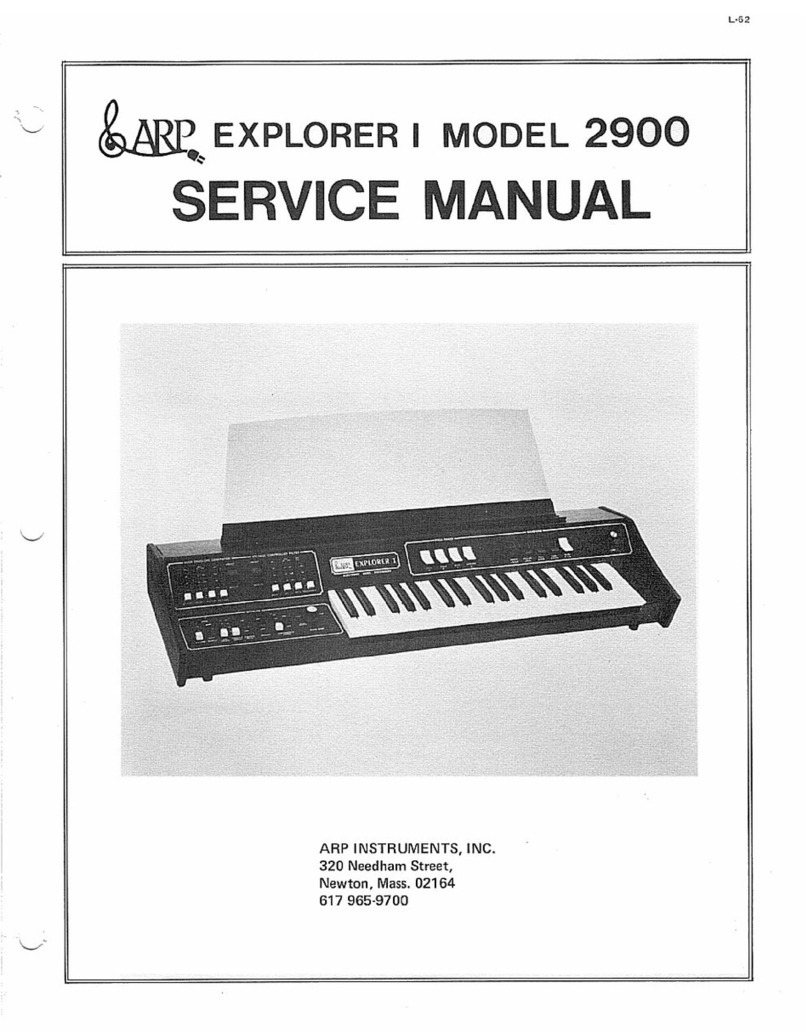
ARP Instruments EXPLORER I 2900 User manual

ARP Instruments
ARP Instruments Odessey 2800 User manual

ARP Instruments
ARP Instruments Quadra User manual

ARP Instruments
ARP Instruments ARP OMNI-2 2471 User manual

ARP Instruments
ARP Instruments Pro Soloist 2701 User manual

ARP Instruments
ARP Instruments 2480 User manual