[AP4470]
200200020-E-01 2020/3
- 2 -
4. Table of Contents
1. General Description ............................................................................................................................ 1
2. Features .............................................................................................................................................. 1
3. Applications......................................................................................................................................... 1
4. Table of Contents ................................................................................................................................ 2
5. Block Diagram..................................................................................................................................... 3
5.1. Block Diagram.............................................................................................................................. 3
5.2. Block Function ............................................................................................................................. 3
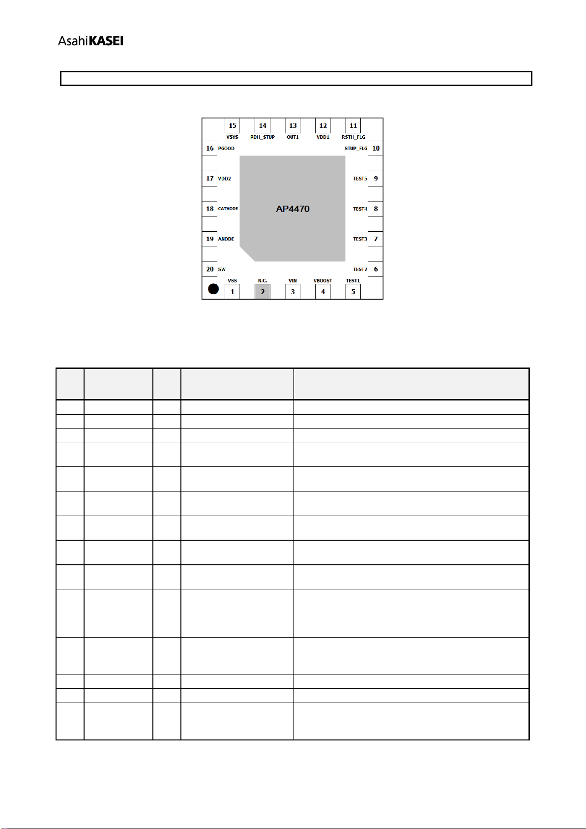
6. Pin Configuration and Function .......................................................................................................... 4
6.1. Pin Configuration ......................................................................................................................... 4
6.2. Pin Function ................................................................................................................................. 4
6.3. The connection of unused pins.................................................................................................... 5
7. Absolute Maximum Ratings ................................................................................................................ 6
8. Recommended Operating Conditions................................................................................................. 7
9. Digital DC Characteristics................................................................................................................... 7
10. Electrical Characteristics ................................................................................................................. 8
11. Description....................................................................................................................................... 9
11.1. Hysteresis comparator 1 (COMP1).......................................................................................... 9
11.1.1 When VDD1 voltage is increasing (Up phase) ........................................................................ 9
11.1.2 When VDD1 voltage is decreasing (Down phase) .................................................................. 9
11.2. Hysteresis comparator 2 (COMP2).......................................................................................... 9
11.3. Startup to DC/DC operation ................................................................................................... 10
11.3.1 Cold Startup ........................................................................................................................... 13
11.3.2 DC/DC .................................................................................................................................... 13
11.3.2.1 When (ISTRG > (IOUT + IVDD1 + IVDD2)).................................................................................... 13
11.3.2.2 When (ISTRG < (IOUT + IVDD1 + IVDD2)).................................................................................... 13
11.4. Power Good ........................................................................................................................... 14
11.5. Startup FLG............................................................................................................................ 15
12. Test Circuits................................................................................................................................... 16
12.1. External Circuit Example........................................................................................................ 16
12.2. PCB Guidline.......................................................................................................................... 17
13. Typical Characteristics .................................................................................................................. 18
13.1. Cold Startup ........................................................................................................................... 18
13.2. Switching Frequency.............................................................................................................. 18
13.3. Low side ON pulse width ....................................................................................................... 19
13.4. COMP1................................................................................................................................... 19
13.5. COMP2................................................................................................................................... 20
13.6. Current consumption.............................................................................................................. 20
13.7. Load curve.............................................................................................................................. 22
14. Recommended External Circuit .................................................................................................... 23
14.1. External Circuit Example........................................................................................................ 23
14.2. Reference PCB ...................................................................................................................... 24
15. Packages....................................................................................................................................... 25
15.1. Outline Dimensions................................................................................................................ 25
15.2. Marking................................................................................................................................... 25
16. Ordering Guide.............................................................................................................................. 26
17. Revision History............................................................................................................................. 26
IMPORTANT NOTICE.............................................................................................................................. 27