Award ECX810 User manual

ECX810
Intel®EP80579
ECX Embedded Board
USER’S MANUAL
Version 1.0

ii
ECX810 User’s Manual
Acknowledgments
Award is a registered trademark of Award Software International,
Inc.
PS/2 is a trademark of International Business Machines
Corporation.
Intel and Intel EP80579 Integrated Processor are registered
trademarks of Intel Corporation.
Microsoft Windows is a registered trademark of Microsoft
Corporation.
Winbond is a registered trademark of Winbond Electronics
Corporation.
All other product names or trademarks are properties of their
respective owners.

ECX810 User’s Manual iii
Table of Contents
Introduction.......................................................1
Product Description.............................................................1
Checklist..............................................................................2
ECX810 Specifications.......................................................3
Board Dimensions...............................................................4
Installations.......................................................5
Installing the Memory.........................................................6
Setting the Jumpers .............................................................7
Connectors on ECX810.....................................................10
BIOS Setup.......................................................21
Drivers Installation......................................41
Appendix...........................................................43
A. Watchdog Timer Configuration ...................................43

iv
ECX810 User’s Manual
This page is intentionally left blank.

INTRODUCTION
1
ECX810 User’s Manual
Introduction
Product Description
The ECX810 ECX (Embedded Compact Extended) board incorporates
the Intel® EP80579 Integrated Processor for Embedded Computing.
The EP80579 Systemon a Chip (SoC) is a new generation processor that
is cost optimized for a wide range of applications. EP80579 delivers the
balance of a powerful IA-32 processor core, standards-based chipset,
and acceleration /communications-focused I/O capabilities.
The EP80579 SoC integrates features into a single device with memory
controller hubs (IMCH) and I/O controller hubs (IICH). The IMCH has
built-in memory controllers for external memory and the IICH has
standard IA I/O peripheral capabilities.
The ECX810’s EP80579 IA-32 core is a derivative of the Intel®
Pentium® M processor. This low power IA-32 core is based on 90-nm
process technology featuring 256-Kbyte L2 cache and 400/533 MHz
quad-pumped internal front-side bus (FSB). With a DDR2 SO-DIMM
socket on board, the board supports up to 2GB of DDR2 system
memory.
It integrates three Gigabit Ethernet MAC interfaces. The MAC fully
implements the IEEE 802.3z, Carrier Sense Multiple Access with
Collision Detection (CSMA/CD) method and physical layer
specifications The GbE features include RGMII/RMII interface to PHY
devices Multi-speed operation 10/100/1000 Mbps
The main features of the ECX810 board are:
Supports Intel EP80579 processors in 600/1066/1200MHz
EP80579 built-in USB 2.0 host controller supports 2 ports
One ports for USB and another for Audio use
EP80579 built-in SATA controller supports 2 ports:
One port for SATA connector and another port for Compact
Flash thru (Acard) serial ATA Bridge Chip ARC772
One DDR2 SDRAM SO-DIMM, Max. 2GB memory
Integrated Three Gigabit Ethernet MACs + PHY
1x SATA, 1x USB 2.0, 4x COM, Watchdog timer,
Interface connector for XGI Daughter board (ID810).
Dimensions of the board are 105mm x 146mm.

INTRODUCTION
2
ECX810 User’s Manual
Checklist
Your ECX810 package should include the items listed below.
•The ECX810 ECX embedded board
•This User’s Manual
•1 CD containing chipset drivers and flash memory utility

INTRODUCTION
ECX810 User’s Manual 3
ECX810 Specifications
Form Factor ECX
CPU Type Intel Architecture (IA-32) processor
CPU Voltage 1.0V ~ 1.3V
CPU Speed 600,1066,1200MHz
CPU Operate Frequency 400MHz/533MHz FSB
Cache 256KB
Green /APM APM1.2
CPU & Chipset Intel EP80579 System on a Chip (SoC)
Integrated Intel® Architecture (IA) processor
and chipset (MCH/ICH) technology
1088-Ball FCBGA package
BIOS Award BIOS, support ACPI Function
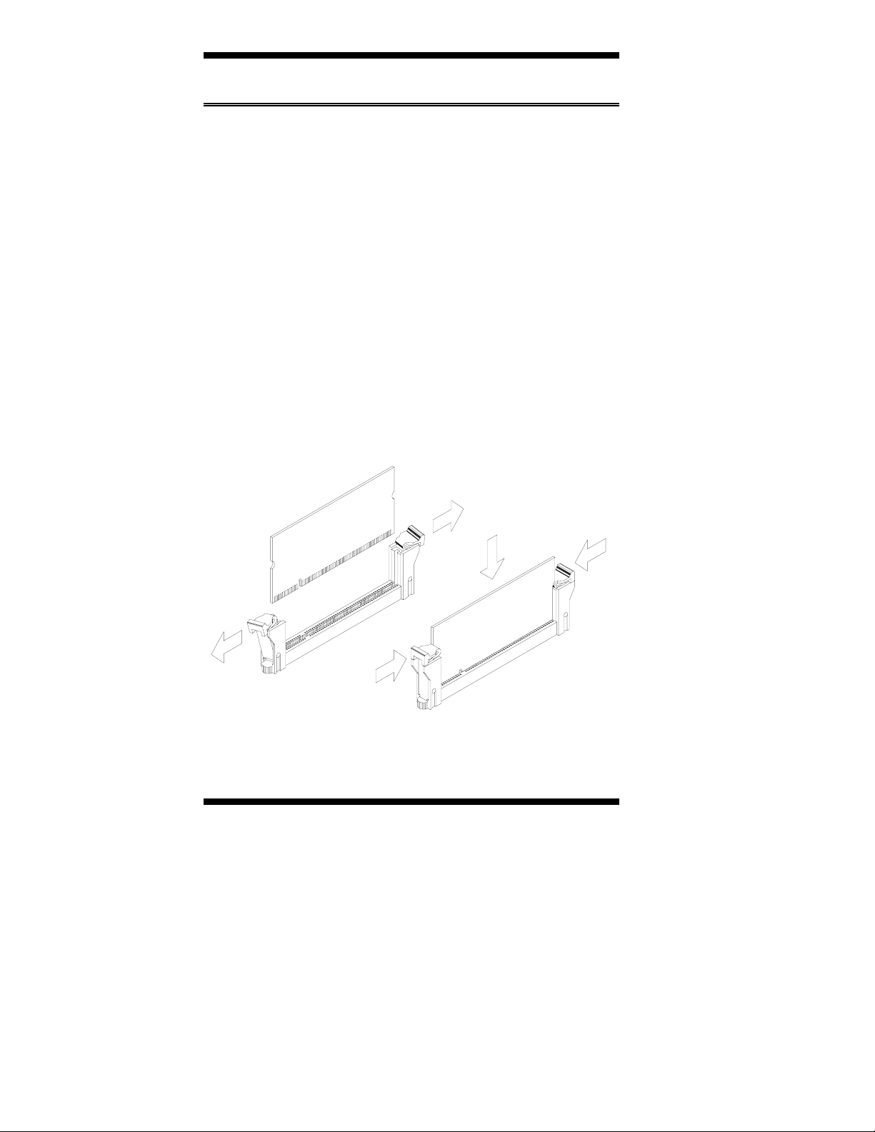
Memory DDR2 400/533/667/800 SO-DIMM x1 (w/o ECC function),
Max. 2GB, (600Mhz CPU at DDR2 667MHz only )
VGA & LVDS Panel XGI /Z11 2D Accelerator 1600 x 1200
PCI-E X 1 bus; Graphic memory DDRII, 32M
Supports CRT (via IB810 daughter board)
Supports 18-bit single channel LVDS (via IB810L daughter
board)
LAN The integrated Three Gigabit Ethernet MACs+ Marvell
88E81145 Gigabit LAN transceiver with 3 x RJ45 Connector
on the board edge
USB (Universal Serial
Bus) EP80579 built-in USB 2.0 host controller
Support 1 port. (Another port occupied for Audio use)
Serial ATA Ports EP80579 built-in SATA controller, supports 2 ports:
One port for SATA Connector, 300MB/s
Another port for CFD thru (Acard) serial ATA Bridge Chip
ARC772(optional)
Compact Flash Acard serial ATA Bridge Chip ARC772 for CF connector
USB Audio USB Audio Codec PCM2902 for Line-out, Line-in
LPC I/O W83627EHG: COM1, COM2 (RS232), & Hardware monitor
(3 thermal inputs, 4 voltage monitor inputs, 1 fan Header)
Digital IO 4 in & 4 out
Keyboard/Mouse Supports PS/2 Keyboard/Mouse connector
Expansion Region Interface connector for XGI VGA Daughter board (ID810)
Edge Connector PS/2 Connector for keyboard/mouse
Gigabit LAN RJ-45 x3
Single USB stack connector
DB9 for COM 1
On Board
Header/Connector 2x15 box-header for COM2.3.4
CF Connector @ solder side(optional)
10-pin header for Digital I/O
SATA connector for SATA port
2x15 header for DB15 VGA Connector (via ID810)
Connector for VGA &DF13-Connector for LVDS (via ID810L)
2x8 header for Front & audio Line-out & Line-in (via ID820)
2x8 header for VPN Front LED (via ID830)
Watchdog Timer Yes (256 segments, 0, 1, 2…255 sec/min)
System Voltage +5V, +3.3V, +12V, 5VSB
Other Modem Wakeup.
Daughter Board
(optional) ID810 - CRT only
ID810L- DF-13 connector
ID820 - Front Connector & Audio Line-in & Line- out
ID830 - VPN RJ45 LED
Board Size 105mm x 146mm

INTRODUCTION
4
ECX810 User’s Manual
[
Board Dimensions
Below are dimensions of the board (top and bottom view.)

INTRODUCTION
ECX810 User’s Manual 5
Installations
This section provides information on how to use the jumpers and
connectors on the ECX810 in order to set up a workable system. The
topics covered are:
Installing the Memory ........................................................................... 6
Setting the Jumpers................................................................................ 7
Connectors on ECX810....................................................................... 10

INTRODUCTION
6
ECX810 User’s Manual
Installing the Memory
The ECX810 supports one DDR2 SO-DIMM memory socket for a
maximum total memory of 2GB, DDR2 400/533/667/800 (w/o ECC
function).
Note: A 600MHz onboard processor will support DDR2 400/533/
667MHz while 1200MHz & 1066MHz processors will support DDR2
400/533/667/800 MHz.
Installing and Removing Memory Modules
To install DDR2 modules, locate the memory socket on the board and
perform the following steps:
1. Hold the DDR2 module so that the keys of the DDR2 module align
with those on the memory slot. Remember to unlock first the clips on
both sides to give way to the memory module.
2. Gently push the DDR2 module in an angle (vertically) as shown in the
picture below until the module reaches the bottom; then lock the
module on both sides of the socket.
3. To remove the module, push the clips outward with both hands.

INTRODUCTION
ECX810 User’s Manual 7
Setting the Jumpers
Jumpers are used on ECX810 to select various settings and features
according to your needs and applications. Contact your supplier if you
have doubts about the best configuration for your needs. The following
lists the connectors on ECX810 and their respective functions.
Jumper Locations on ECX810............................................................... 8
JP2: AT (Emulation)/ATX Power Selection ......................................... 9
JP4: Clear CMOS Setting...................................................................... 9
JP5, JP6: CAN Bus Termination Setting (Reserved) ............................ 9

INTRODUCTION
8
ECX810 User’s Manual
Jumper Locations on ECX810
AT/ATX Power
Selection
Clear CMOS Setting
CANBus
Termination
Setting
(Reserved)
Jumper Locations on ECX810.................................................. Page
JP2: AT(Emulation) /ATX Power Selection...................................9
JP4: Clear CMOS Setting...............................................................9
JP5, JP6: CAN Bus Termination Setting (Reserved)......................9

INTRODUCTION
ECX810 User’s Manual 9
JP2: AT (Emulation)/ATX Power Selection
JP2 Power Select
AT (Emulation)
ATX
Note: AT (Emulation) does not require pressing the power button to turn
on the system; plugging the AC power will turn on the system.
JP4: Clear CMOS Setting
JP4 Setting
Normal
Clear CMOS
JP5, JP6: CAN Bus Termination Setting (Reserved)
JP5, JP6 Setting
Terminate Bus
No Terminate Bus

INTRODUCTION
10
ECX810 User’s Manual
Connectors on ECX810
The connectors on ECX810 allows you to connect external devices such
as keyboard, floppy disk drives, hard disk drives, printers, etc. The
following table lists the connectors on ECX810 and their respective
functions.
Connector Locations on ECX810........................................................11
CN1: Serial ATA Connector................................................................12
CN2, CN3, CN4: Gigabit LAN RJ-45.................................................12
CN5: PS/2 Keyboard and PS/2 Mouse Connectors.............................12
CN6: USB1 Port Connector.................................................................12
CN7: COM1 Connector.......................................................................12
CN8: Compact Flash Connector (optional) .........................................12
CPUFAN1: System Fan Power Connector..........................................12
J1: LAN LED Pin Header....................................................................13
J3: Power Supply Connector................................................................13
J4: SO-DIMM Socket..........................................................................14
J6: VGA Daughter Board Interface Connector....................................14
J7: IEEE1588 Pin Header (Reserved)..................................................16
J8: GPIO Pin Header (Reserved).........................................................17
J9: SPI Pin Header (Debug Only)........................................................17
J10: Digital I/O Pin Header .................................................................17
J11: Front Pin Header..........................................................................17
J12: VGA Pin Header..........................................................................18
J13: CAN Bus Port1 Pin Header (Reserved).......................................18
J14: COM2/3/4 is a 30-pin Header......................................................19
J15: CAN Bus Port2 Pin Header (Reserved).......................................19
J16: LPC 80 Port Pin Header (Debug Use Only) ................................20

INTRODUCTION
ECX810 User’s Manual 11
Connector Locations on ECX810

INTRODUCTION
12
ECX810 User’s Manual
CN1: Serial ATA Connector
CN2, CN3, CN4: Gigabit LAN RJ-45
CN5: PS/2 Keyboard and PS/2 Mouse Connectors
CN5 uses a Y-cable with dual D-connectors for a PS/2 keyboard and a
PS/2 mouse.
Pin # Signal Name
1 Mouse data
2 Keyboard data
3 Ground
4 Vcc
5 Mouse Clock
6 Keyboard Clock
CN6: USB1 Port Connector
CN7: COM1 Connector
[ Signal Name Pin # Pin # Signal Name
DCD 1 6 DSR
RXD 2 7 RTS
TXD 3 8 CTS
DTR 4 9 RI
GND 5 10 Not Used
CN8: Compact Flash Connector (optional)
CPUFAN1: System Fan Power Connector
CPUFAN1 is a 3-pin header for system fans. The fan must be a 12V
(500mA).
Pin # Signal Name
1 Ground
2 +12V
3 Rotation detection

INTRODUCTION
ECX810 User’s Manual 13
J1: LAN LED Pin Header
This is for the optional ID830 Front VPN LED module (shown below) is
suitable for use in VPN appliance. J1 is connected to ID830 with the
EXT109 (150mm) cable.
Signal Name Pin Pin Signal Name
P0_LED_TX 1 2 P1_LED_TX
P0_LINK1000 3 4 P1_LINK1000
P0_LINK100 5 6 P1_LINK100
P2_LINK1000 7 8 P2_LED_TX
P2_LINK100 9 10 P2V5_AUX
GPIO 11 12 GP24
GND 13 14 +3.3V
GPIO or
HDD_LED 15 16 Cut Pin
J3: Power Supply Connector
Use power cable (PW71) to connect to ATX Power Supply.
Pin # Signal Name
1 PS-ON
2 Ground
3 Ground
4 +12V
5 +3.3V
6 Ground
7 +3.3V
8 +5V
9 +5V
10 5VSB

INTRODUCTION
14
ECX810 User’s Manual
J4: SO-DIMM Socket
The ECX810 supports one DDR2 SO-DIMM socket for a maximum
memory of 2GB, DDR2 400/533/667/800 (w/o ECC function).
Note: A 600MHz onboard processor will support DDR2
400/533/667MHz while 1200MHz & 1066MHz processors will support
DDR2 400/533/667/800MHz.
J6: VGA Daughter Board Interface Connector
J6 is designed for the ID810 (shown and described below) XGI VGA
daughter board that supports CRT and 18-bit LVDS displays. However, the
CRT VGA cable is to be connected to the J12 pin header on the board.
ID810 XGI VGA daughter board

INTRODUCTION
ECX810 User’s Manual 15
ID810 supports CRT only; it does not support LVDS
ID810L, for 18bit LVDS transmitters,supports TFT LCD
panel with 800x480 resolution. This resolution is
manufacturer’s default. For other resolutions, please contact
your sales dealer for assistance.
J1: Backlight Control Connectors
Pin # Signal Name
1 +12V
2 Backlight Enable
3 Backlight VRB
4 Ground
J2: Support 18 bits single channel LVDS Connectors
Signal Name Pin # Pin # Signal Name
TX0- 2 1 TX0+
Ground 4 3 Ground
TX1- 6 5 TX1+
5V/3.3V 8 7 Ground
N.C 10 9 N.C
TX2- 12 11 TX2+
Ground 14 13 Ground
TXCLK- 16 15 TXCLK+
5V/3.3V 18 17 ENABKL
+12V 20 19 +12V
*Depends on JP1 setting (1-2 for 3.3V/default, 2-3 for 5V).
Remarks: J2 supports TFT LCD panel model such as Hitachi
TX18D11VM with 18 bit LVDS, resolution of 800x480 pixel
JP1: LVDS VDD Select (5V / 3.3V)
JP1 VDD Setting
3.3V
5V

INTRODUCTION
16
ECX810 User’s Manual
CN1: LED Backlight TFT LCD Connectors (Optional)
CN1 supports LED Backlight TFT LCD panel such as in CPT
model SCLAA070LC0ECW with 18 bit LVDS, resolution of
800x480 pixel
Signal Name Pin #
+3.3V 1
+3.3V 2
+3.3V 3
N.C. 4
Backlight VRB 5
N.C. 6
Ground 7
TX0- 8
TX0+ 9
Ground 10
TX1- 11
TX1+ 12
Ground 13
TX2- 14
TX2+ 15
Ground 16
TXCLK- 17
TXCLK+ 18
Ground 19
N.C. 20
N.C. 21
Ground 22
N.C. 23
+5V 24
+5V 25
+5V 26
N.C. 27
Ground 28
N.C. 29
N.C 30
J7: IEEE1588 Pin Header (Reserved)
Signal Name Pin Pin Signal Name
TSTMDA 1 2 TS_PPS
ASMSIG 3 4 AMMSIG
RX_SNP 5 6 TX_SNP
GND 7 8 GND
Table of contents
Other Award Computer Hardware manuals
Popular Computer Hardware manuals by other brands

Qiyang
Qiyang GF-RK3399-CM Hardware manual

EK-Quantum
EK-Quantum Reflection Fractal ATX D5 PWM D-RGB - Plexi user guide

Key Digital
Key Digital HD Leeza KD-HD1080P Quick setup guide

Dynisco
Dynisco UPR700 Installation and operation manual

Becom
Becom Argos3D-P230 Hardware user manual

Conrad
Conrad DVD-Creator USB2.0 operating instructions

Dell EMC
Dell EMC Q-SYS 5200-G2 quick start guide

Acrosser Technology
Acrosser Technology AR-B5890 user manual

ST-Ericsson
ST-Ericsson UM10032 user manual

ekwb
ekwb EK-FC Strix RTX 2080 Ti Backplate Classic Installation and mounting manuals

Freescale Semiconductor
Freescale Semiconductor MCF5329 Reference manual

Asus
Asus AAEON BOXER-8224AI user manual