AWINIC AW86225 User manual

AW86225
October 2021 V1.9
www.awinic.com 1 Copyright © 2020 SHANGHAI AWINIC TECHNOLOGY CO., LTD
Low Power F0 Detect and Tracking LRA Haptic Driver
Features
1MHz I2C Bus
Integrated 3K Memory
12k/24k/48k input wave sampling rate
F0 detect and tracking
Advance autobrake engine integrated
Playback mode:
Real time playback
Memory playback
1 Trigger playback
Cont playback
Resistance-Based LRA Diagnostics
Drive signal monitor for LRA protect
Drive Compensation Over Battery Discharge
Fast Start Up Time <0.4ms
Reused interrupt output pin
Support automatically switch to standby mode
Standby current:3uA
Shutdown current:<1uA
Supply voltage range 3 to 5.5V
Short-Circuit Protection, Over-Temperature
Protection, Under-Voltage Protection
WLCSP 1.127mmX1.127mmX0.557mm-9B
Package
Applications
Mobile phones
Tablets
Wearable Devices
General Description
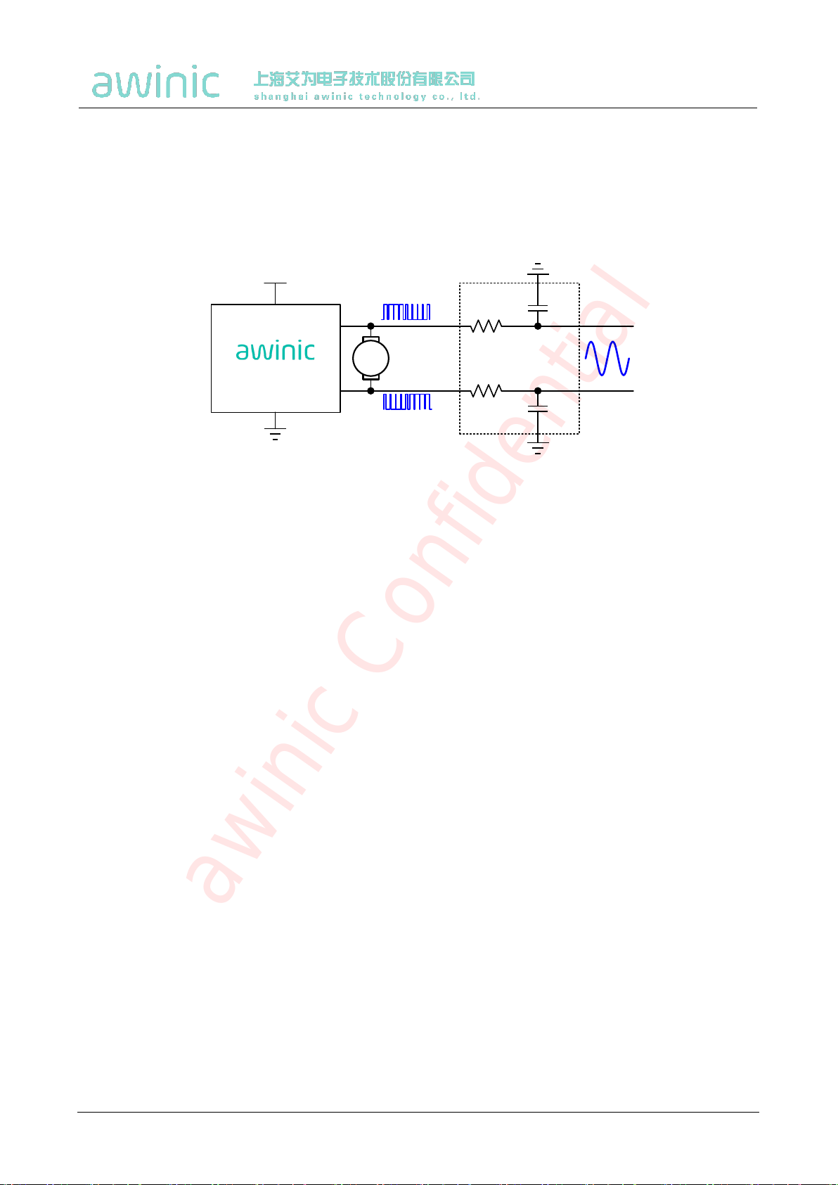
AW86225 is a low cost H-bridge, single chip LRA
haptic driver, with F0 detecting and tracking based
on BEMF, supporting real time playback, memory
playback, Cont playback and hardware pin trigged
playback with fast start up time. All these make the
AW86225 an ideal candidate for haptic driver.
AW86225 integrates a 3KByte SRAM for user-
defined waveforms to achieve a variety of
vibration experiences, supporting 3 sampling
rate(12k/24k/48k) of waveforms loaded in SRAM,
supporting output waveform sampling rate up-
sampling to 48k.
AW86225 integrates an autobrake engine to
suppress the aftershocks to zero for different drive
waveforms (short or long) on different LRA
motors.
AW86225 supports LRA fault diagnostic based on
resistance measurement and protections of short-
circuit, over-temperature and under-voltage.
AW86225 features configurable automatically
switch to standby mode after haptic waveform
playback finished. This can less quiescent power
consumption. The RSTN pin provides further
power saving by fully shut down the whole device.
Reused interrupt output pin can detect real time
FIFO status and the error status of the chip.
AW86225 features general settings are
communicated via an I2C-bus interface.
AW86225 is available in a WLCSP
1.127mmX1.127mmX0.557mm-9B package.
All trademarks are the property of their respective owners.
awinic Confidential

AW86225
October 2021 V1.9
www.awinic.com 2 Copyright © 2020 SHANGHAI AWINIC TECHNOLOGY CO., LTD
Pin Configuration and Top Mark
QXQ
XXX
XXX
QXQ - AW86225CSR
XXX - Production Tracing Code
AW86225CSR Marking
(Top View)
AW86225CSR
(Top View)
Figure 1 Pin Configuration and Top Mark
Pin Definition
PIN NUMBER
NAME
TYPE(1)
DESCRIPTION
A1
TRIG/INTN
I/O
Multi-mode pin. Selectable as input trigger (pulse), or output interrupt
Default function is INTN, when set as interrupt output, there must be
a pullup resistance to be added.
B1
SDA
I/O
I2C bus data input/output(open drain)
C1
SCL
I
I2C bus clock input
A2
VREG
Power
Output of LDO
B2
RSTN
I
Active low hardware reset
High: standby/active mode Low: power-down mode
C2
VDD
Power
Chip power supply
A3
HDP
O
Positive haptic driver differential output
B3
GND
Ground
Supply ground
C3
HDN
O
Negative haptic driver differential output
awinic Confidential

AW86225
October 2021 V1.9
www.awinic.com 3 Copyright © 2020 SHANGHAI AWINIC TECHNOLOGY CO., LTD
Functional Block Diagram
OSC
OTP
BIAS
OCP
UVLO
Driver
LDO
(1.8V)
HDP
HDN
SCL
SDA
GND VREG
TRIG/INTN
VDD
LRA
RSTN
RL_DE
T
Logic
I2C
interface
Trig
interface
Wave
editor
DPWM
Main
control
Auto
brake F0
tracking
SRAM
HSRC
BEMF Detection
LRA Diagnosis
Figure 2 FUNCTIONAL BLOCK DIAGRAM
Typical Application Circuits
VDD
AW86225
VDD
TRIG/INTN
HDP
HDN
GND
C3
10uF
C2
0.1uF
VREG
C1
0.1uF
LRA
B3
A3
C3
C2
A2
A1
SDA
B1
SCL
C1
B1
C4
0.1nF
B2
C5
0.1nF
RSTN
B2
GPIO
VIO
R1
4.7kΩ
R2
4.7kΩ
VIO
SCL
SDA
VIO
GPIO
R3
4.7kΩ
Figure 3 Typical Application Circuit of AW86225
All trademarks are the property of their respective owners.
awinic Confidential

AW86225
October 2021 V1.9
www.awinic.com 4 Copyright © 2020 SHANGHAI AWINIC TECHNOLOGY CO., LTD
Notice for Typical Application Circuits:
1: Please place C1,C2,C3 as close to the chip as possible. The capacitors should be placed in the same
layer with the AW86225 chip.
2: For the sake of driving capability, the power lines (especially the one to VDD) and output lines should be
short and wide as possible.
Ordering Information
Part
Number
Temperature
Package
Marking
Moisture
Sensitivity
Level
Environment
Information
Delivery
Form
AW86225CSR
-40°C~85°C
WLCSP
1.127mmX1.127mmX0.557mm-
9B
QXQ
MSL1
ROHS+HF
4500 units/
Tape and
Reel
awinic Confidential

AW86225
October 2021 V1.9
www.awinic.com 5 Copyright © 2020 SHANGHAI AWINIC TECHNOLOGY CO., LTD
Absolute Maximum Ratings(NOTE 1)
PARAMETERS
RANGE
Supply voltage range VDD
-0.3V to 6.0V
HDP, HDN, TRIG/INTN
-0.3V to VDD+0.3V
SDA, SCL, RSTN
-0.3V to 6.0V
Minimum load resistance RL
5Ω
Junction-to-ambient thermal resistance a
132°C/W
Operating free-air temperature range
-40°C to 85°C
Maximum Junction Temperature TJMAX
150°C
Storage Temperature Range TSTG
-65°C to 150°C
Lead Temperature(Soldering 10 Seconds)
260°C
ESD(Including CDM)(NOTE 2 3)
HBM(Human Body Model)
±2KV
CDM(Charge Device Model)
±1.5KV
Latch-up
Test Condition: JEDEC EIA/JESD78E
+IT: 200mA
-IT: -200mA
NOTE 1: Conditions out of those ranges listed in "absolute maximum ratings" may cause permanent
damages to the device. In spite of the limits above, functional operation conditions of the device should
within the ranges listed in "recommended operating conditions". Exposure to absolute-maximum-rated
conditions for prolonged periods may affect device reliability.
NOTE 2
:
The human body model is a 100pF capacitor discharged through a 1.5kΩ resistor into each pin.
Test method: ANSI/ESDA/JEDEC JS-001-2017.
NOTE 3
:
Charge Device Model test method: ANSI/ESDA/JEDEC JS-002-2018.
awinic Confidential

AW86225
October 2021 V1.9
www.awinic.com 6 Copyright © 2020 SHANGHAI AWINIC TECHNOLOGY CO., LTD
Electrical Characteristics
Characteristics
Test condition: TA=25°C,VDD=3.6V,RL=8Ω+100μH,f=160Hz (unless otherwise noted)
Symbol
Description
Test Conditions
Min
Typ.
Max
Units
VVDD
Battery supply voltage
On pin VDD
3
5.5
V
VVREG
Voltage at VREG pin
1.8
V
VIL
Logic input low level
RSTN/TRIG/INTN/SCL/SDA
0.5
V
VIH
Logic input high level
RSTN/TRIG/INTN/SCL/SDA
1.3
V
VOL
Logic output low level
TRIG/INTN/SDA
IOUT=4mA
0.4
V
VOS
Output offset voltage
I2C signal input 0
-30
0
30
mV
ISD
Shutdown current
RSTN =0V
0.1
1
μA
ISTBY
Standby current
RSTN=1.8V
3
μA
IQ
Quiescent current
1
mA
UVP
Under-voltage protection
voltage
2.7
V
Under-voltage protection
hysteresis voltage
100
mV
TSD
Over temperature
protection threshold
160
°C
TSDR
Over temperature
protection recovery
threshold
130
°C
TON1
Time from shutdown to
standby
3
ms
TON2
Waveform startup time
From trigger to output signal
0.4
ms
HDRIVER
Rdson
Drain-Source on-state
resistance
Include NMOS and PMOS,
VDD=4.2V
750
mΩ
Rocp
Load impedance
threshold for over current
protection
2
Ω
FPWM
PWM output frequency
VDD=4.2V, PD_HWM=0
96
kHz
VDD=4.2V, PD_HWM=1
48
kHz
FCALI_ACC_LRA
LRA Consistency
Calibration accuracy
F0-2
F0
F0+2
Hz
Vpeak
Output voltage
RL=8Ω+100μH
VDD=4.2V
3.6
V
Output voltage
RL=16Ω+100μH
3.8
V
awinic Confidential

AW86225
October 2021 V1.9
www.awinic.com 7 Copyright © 2020 SHANGHAI AWINIC TECHNOLOGY CO., LTD
VDD=4.2V
I2C Interface Timing
Parameter
fast mode
fast mode plus
UNIT
No.
Symbol
Name
MIN
TYP
MAX
MIN
TYP
MAX
1
fSCL
SCL Clock frequency
400
1000
kHz
2
tLOW
SCL Low level Duration
1.3
0.5
μs
3
tHIGH
SCL High level Duration
0.6
0.26
μs
4
tRISE
SCL, SDA rise time
0.3
0.12
μs
5
tFALL
SCL, SDA fall time
0.3
0.12
μs
6
tSU:STA
Setup time SCL to START state
0.6
0.26
μs
7
tHD:STA
(Repeat-start) Start condition hold time
0.6
0.26
μs
8
tSU:STO
Stop condition setup time
0.6
0.26
μs
9
tBUF
the Bus idle time START state to STOP
state
1.3
0.5
μs
10
tSU:DAT
SDA setup time
0.1
0.1
μs
11
tHD:DAT
SDA hold time
10
10
ns
SCL
SDA
tHIGH tLOW
tSU:DAT tHD:DAT
tRISE tFALL
(2)(3)
(4) (5)
(10) (11)
Figure 4 SCL and SDA timing relationships in the data transmission process
SCL
SDA
tSU:STA
tHD:STA
(6)
(7)
tSU:STO
(8)
tBUF
(9)
Figure 5 The timing relationship between START and STOP state
awinic Confidential

AW86225
October 2021 V1.9
www.awinic.com 8 Copyright © 2020 SHANGHAI AWINIC TECHNOLOGY CO., LTD
Measurement Setup
AW86225 features switching digital output, as shown in Figure 6. Need to connect a low pass filter to HDP/HDN
output respectively to filter out switch modulation frequency, then measure the differential output of filter to
obtain analog output signal.
HDP
HDN
AW86225
3.4kHz
Low-Pass Fliter
100kΩ
100kΩ
0.47nF
0.47nF
LRA
Figure 6 AW86225 test setup
awinic Confidential

AW86225
October 2021 V1.9
www.awinic.com 9 Copyright © 2020 SHANGHAI AWINIC TECHNOLOGY CO., LTD
Typical Characteristics
Figure 7 Standby Current Vs Supply Voltage
Figure 9 Trig Application
Figure 8 LRA with Automatic Braking
Figure 10 Automatic Resonance Tracking
1
1.5
2
2.5
3
3.5
2.5 3 3.5 4 4.5 5 5.5 6
Standby Current(uA)
Supply Vlotage(V)
awinic Confidential

AW86225
October 2021 V1.9
www.awinic.com 10 Copyright © 2020 SHANGHAI AWINIC TECHNOLOGY CO., LTD
Detailed Functional Description
Power On Reset
The device provides a power-on reset feature that is controlled by LDO_OK. The reset signal will be generated
to perform a power-on reset operation, which will reset all circuits and configuration registers. When the VDD
power on, the VREG voltage raises and produce the LDO_OK indication, the reset is over.
Operation Mode
The device supports 3 operation modes.
Table 1 Operating Mode
Mode
Condition
Description
Power-Down
VDD = 0V or RSTN = 0V
Power supply is not ready or RSTN is tie to low.
Whole chip shutdown including I2C interface.
Standby
VDD > 2.7V
and RSTN = HIGH
and no wave is going
Power supply is ready and RSTN is tie to high.
Most parts of the device are power down for low power
consumption except I2C interface and LDO.
Active
Playing a waveform
Most parts of the device are working
Power supply OK
(VVDD > 2.7V)
And RSTN = 1
Power-down
Standby Active
Powersupply not ready
(VVDD = 0) or RSTN = 0
Starta play request
Waveform is over
orset a softrstn
Powersupply not ready
(VVDD = 0) or RSTN = 0
Figure 11 Device operating modes transition
POWER-DOWN MODE
The device switches to power-down mode when the supply voltage is not ready or RSTN pin is set to low.
In this mode, all circuits inside this device will be shut down. I2C interface isn’t accessible in this mode, and all
of the internal configurable registers and Memory are cleared.
The device will jump out of the power-down mode automatically when the supply voltages are OK and RSTN
awinic Confidential

AW86225
October 2021 V1.9
www.awinic.com 11 Copyright © 2020 SHANGHAI AWINIC TECHNOLOGY CO., LTD
pin is set to high.
Standby Mode
The device switches standby mode when the power supply voltages are OK and RSTN pin set to high. In this
mode I2C interface is accessible, other modules except LDO module are still powered down. Customer can
force device to this mode by setting STANDBY to high. Also in this mode, customer can initialize waveform
library in SRAM. Device will be switched to this mode after haptic waveform playback finished.
Active Mode
The device is fully operational in this mode. H-bridge driver circuits will start to work. Users can send a playback
request to make device in this mode.
Power On And Power Down Sequence
This device power on sequence is illustrated in the following figure:
RSTN
3ms
I2C
VDD
I2C configuration
100 μs 100 μs
Figure 12 Power On Sequence
Playback Sequence
Make sure the device is not in POWER-DOWN MODE before sending a playback request, then the playback
sequence is illustrated in the following figure:
awinic Confidential

AW86225
October 2021 V1.9
www.awinic.com 12 Copyright © 2020 SHANGHAI AWINIC TECHNOLOGY CO., LTD
Set EN_RAMINIT = 1
Downloadwaveform to
SRAM
RAM mode config RTP mode configCONT mode config
Set GO=1 Set GO=1 Set GO=1Send a trigger
Wait 1ms
Wait
GLB_STATE=4'b1000
Power on
CONT MODE RAM MODE TRIG MODE RTP MODE
Set EN_RAMINIT = 0
Global configuration
Receive aPlayback Request
Write data toRTP FIFO
Figure 13 Power up and playback sequence
Software Reset
Writing 0xAA to register SRST(0x00) via I2C interface will reset the device internal circuits except SRAM,
including configuration registers.
Battery Voltage Detect
Software can send command to detect the battery voltage.
Detect steps:
Set EN_RAMINIT to 1 in register 0x43;
awinic Confidential

AW86225
October 2021 V1.9
www.awinic.com 13 Copyright © 2020 SHANGHAI AWINIC TECHNOLOGY CO., LTD
Set VBAT_GO to 1 in register 0x52;
Wait 3ms;
Set EN_RAMINIT to 0 in register 0x43;
Read VBAT in register 0x55 and VBAT_LO in register 0x57.
The code is a 10bit unsigned number.
𝑉𝐷𝐷 = 6.1 × (𝑉𝐵𝐴𝑇 × 4 + 𝑉𝐵𝐴𝑇_𝐿𝑂)
1024 (𝑉)
Constant Vibration Strength
The device features power-supply feedback. If the supply voltage discharge over time, the vibration strength
remains the same as long as enough supply voltage is available to sustain the required output voltage. It is
especially useful for ring application. Power-supply feedback only works in CONT playback mode.
Use steps:
Set VBAT_MODE to 1 in register 0x43;
Initiates a CONT playback request.
LRA Consistency Calibration
Different motor batches, assembly conditions and other factors can result in f0 deviation of LRA. When the
drive waveform does not match the LRA monomer, the vibration may be inconsistent and the braking effect
becomes worse, especially for short vibration waveforms. So it's necessary to perform consistency calibration
of LRA. Firstly, the power-on f0 detection can be launched to get the f0 of LRA. Secondly the waveform
frequency stored in SRAM and the f0 of LRA are used to calculate the code for calibration. The f0 accuracy
after LRA consistency calibration is ±2Hz.
LRA Resistance Detect
Software can send command to detect the LRA’s resistance.
Detect steps:
Set EN_RAMINIT to 1 in register 0x43;
Read D2S_GAIN register and save the result as d2s_gain_pre;
Set D2S_GAIN with an appropriate with in register 0x49;
Set RL_OS to 1 in register 0x51;
Set DIAG_GO to 1 in register 0x52;
Wait 3ms;
Set EN_RAMINIT to 0 in register 0x43;
Restore the value of D2S_GAIN register to d2s_gain_pre;
Read RL in register 0x53 and RL_LO in register 0x57.
Based on this information host can diagnosis used LRA’s status. The code is a 10bit unsigned number.
𝑅𝐿 =678 × (𝑅𝐿 × 4 + 𝑅𝐿_𝐿𝑂)
1024 ×D2S_GAIN (𝛺)
The values of the D2S_GAIN that can be configured for different sizes of RL are listed below. The higher the
awinic Confidential

AW86225
October 2021 V1.9
www.awinic.com 14 Copyright © 2020 SHANGHAI AWINIC TECHNOLOGY CO., LTD
RL, the smaller the configurable D2S_GAIN.
Table 2 D2S_GAIN Selection
RL(Ω)
D2S_GAIN
2~30
20
31~60
10
Flexible Haptic Data Playback
The device offers multiple ways to playback haptic effects data. The PLAY_MODE bits select RAM mode, RTP
mode, CONT mode. Additional flexibility is provided by the one hardware TRIG pins, which can override
PLAY_MODE bit to playback haptic effects data as configuration.
The device contains 3 kB of integrated SRAM to store customer haptic waveforms’ data. The whole SRAM is
separated to RAM waveform library and RTP FIFO region by base address. And RAM waveform library is
including waveform library version, waveform header and waveform data.
0
BFF
Action1
Action127
WAV DATA
WAVFORM
HEADER
BASE_ADDR Waveform version
Start address high
Start address low
End address high
End address low
Start address high
Start address low
End address high
End address low
WAVFORM DATA
RTP FIFO
Figure 14 Data structure in SRAM
SRAM mode and TRIG mode playback the waveforms in RAM waveform library and RTP mode playback the
waveform data written in RTP FIFO, CONT mode playback non-filtered or filtered square wave with rated drive
voltage.
Sram Structure
A RAM waveform library consists of a waveform version byte, a waveform header section, and the waveform
data content. The waveform header defines the data boundaries for each waveform ID in the data field, and
the waveform data contains a signed data format (2's complement) to specify the magnitude of the drive.
awinic Confidential

AW86225
October 2021 V1.9
www.awinic.com 15 Copyright © 2020 SHANGHAI AWINIC TECHNOLOGY CO., LTD
3FF
WAVEFORM SRAM
Waveform library version
Waveform#N start address high
Waveform#N start address low
Waveform#N end address high
Waveform#N end address low
base_addr
Waveform#2 start address high
Waveform#2 start address low
Waveform#2 end address high
Waveform#2 end address low
Waveform#1 start address high
Waveform#1 start address low
Waveform#1 end address high
Waveform#1 end address low
0
#1
#2
#N
4 * (#1 –1)+ 1
4 * (#1 –1)+ 2
4 * (#1 –1)+ 3
4 * (#1 –1)+ 4
4 * (#2 –1)+ 1
4 * (#2 –1)+ 2
4 * (#2 –1)+ 3
4 * (#2 –1)+ 4
4 * (#N –1)+ 1
4 * (#N –1)+ 2
4 * (#N –1)+ 3
4 * (#N –1)+ 4
4 * (#N –1)+ 5
4 * (#N –1)+ 4 + len(#1)
4 * (#N –1)+ 5 + len(#1)
4 * (#N –1)+ 4 + len(#1) + len(#2)
...
...
address
Figure 15 Waveform library data structure
Waveform version:
One byte located on SRAM base address, setting to different value to identify different version of RAM
waveform library.
Waveform header:
The waveform header block consist of N-boundary definition blocks of 4 bytes each. N is the number of
waveforms stored in the SRAM (N cannot exceed 127). Each of the boundary definition blocks contain the
start address (2 bytes) and end address (2 bytes). So the total length of waveform header block are N*4 bytes.
The start address contains the location in the memory where the waveform data associated with this waveform
begins.
The end address contains the location in the memory where the waveform data associated with this waveform
ends.
The waveform ID is determined after base address is defined. Four bytes begins with the address next to base
address are the first waveform ID’s header, and next four bytes are the second waveform ID’s header, and so
on.
Waveform data:
The waveform data contains a signed data format (2's complement) to specify the magnitude of the drive. The
begin address and end address is specified in waveform ID’s header.
Waveform library initialization steps:
Prepare waveform library data including: waveform library version, waveform header fields for waveform
in library and waveform data of each waveform;
Set register EN_RAMINIT=1 in register 0x43, to enable SRAM initial;
Set base address (register 0x2D, 0x2E);
Write waveform library data into register 0x42 continually until all the waveform library data written;
Set register EN_RAMINIT=0, to disable SRAM initial;
awinic Confidential

AW86225
October 2021 V1.9
www.awinic.com 16 Copyright © 2020 SHANGHAI AWINIC TECHNOLOGY CO., LTD
Ram Mode
To playback haptic data with RAM mode, the waveform ID must first be configured into the waveform playback
queue and then the waveform can be played by writing GO bit register.
WAVSEQ1
WAVSEQ2
WAVSEQ3
WAVSEQ4
GO
Waveform 1
Waveform 2
Waveform 3
Waveform N
Waveform libraryPLAYBACK QUEUE
WAVSEQ5
WAVSEQ6
WAVSEQ7
WAVSEQ8
.
.
.
Figure 16 RAM mode playback
The waveform playback queue defines waveform IDs in waveform library for playback. Eight WAVSEQx
registers queue up to eight library waveforms for sequential playback. A waveform ID is an integer value
referring to the index of a waveform in the waveform library. Playback begins at WAVSEQ1 when the user
triggers the waveform playback queue. When playback of that waveform ends, the waveform queue plays the
next waveform ID held in WAVSEQ2 (if non-zero). The waveform queue continues in this way until the queue
reaches an ID value of zero or until all eight IDs are played whichever comes first.
The waveform ID is a 7-bit number. The MSB of each ID register can be used to implement a delay between
queue waveforms. When the MSB is high, bits 6-0 indicate the length of the wait time. The wait time for that
step then becomes WAVSEQ[6:0] × wait_time unit. Wait_time unit can be configuration of WAITSLOT register.
The device allows for looping of individual waveforms by using the SEQxLOOP registers. When used, the state
machine will loop the particular waveform the number of times specified in the associated SEQxLOOP register
before moving to the next waveform. The device allows for looping of the entire playback sequence by using
the MAIN_LOOP register. The waveform-looping feature is useful for long, custom haptic playbacks, such as
a haptic ringtone.
Playback steps:
Waveform library must be initialized before playback;
Set PLAY_MODE bit to 0 in register 0x08;
Set playback queue registers (0x0A ~ 0x11) as desired;
Set playback loop registers (0x12~ 0x16) as desired;
Set GO bit to 1 in register 0x09 to trigger waveform playback;
Device will be switched to STANDBY mode after haptic waveform playback finished.
awinic Confidential

AW86225
October 2021 V1.9
www.awinic.com 17 Copyright © 2020 SHANGHAI AWINIC TECHNOLOGY CO., LTD
Rtp Mode
The real-time playback mode is a simple, single 8-bit register interface that holds an amplitude value. When
real-time playback is enabled, begin to enters a register value to RTP_DATA over the I2C will trigger the
playback, the value is played until the data sending finished or removes the device from RTP mode.
After FF_AEM or FF_AFM register is configured as 0, HOST can obtain the RTP FIFO almost empty or almost
full status through interrupt signal(pin INTN) or read FF_AES or FF_AFS register. RTP FIFO almost empty and
almost full threshold can be configured through FIFO_AE and FIFO_AF registers.
Figure 17 RTP mode playback
Playback steps:
Prepare RTP data before playback;
Set PLAY_MODE bit to 1 in register 0x08;
Set GO bit to 1 in register 0x09 to trigger waveform playback;
Delay 1ms;
Check GLB_STATE=4’b1000, if HOST don’t send data to FIFO, chip will wait for RTP data coming in this
state forever;
Write RTP data continually to register 0x32 to playback RTP waveform;
HOST need monitor the full and empty status for RTP FIFO.
Device will be switched to STANDBY mode after wave data in RTP FIFO is played empty.
Trig Mode
The device has a configuration, multi-mode pin TRIG/INTN. It can serve as a dedicated hardware pin for quickly
trigger haptic data playback through configuration register INTN_PIN. Quickly trigger can be configured
posedge/negedge/both-edge/level trigger.
FIFO
Almost empty threshold
Almost full level
FIFO write address
FIFO read address
FIFO last address
0
FIFO NOT empty and
chip startup FIFO empty
... ...
awinic Confidential

AW86225
October 2021 V1.9
www.awinic.com 18 Copyright © 2020 SHANGHAI AWINIC TECHNOLOGY CO., LTD
Figure 18 TRIG mode playback
Edge mode or level mode is accessible through configuration register TRG1_LEV. When an edge mode is
needed, user should set TRG1_LEV =0. In edge mode, register TRG1SEQ_P and TRG1_POS respectively
represent the waveform and enable signal of positive edge, where register TRG1SEQ_N and TRG1_NEG
respectively represent the waveform and enable signal of negative edge.
When a level mode is needed, user should set TRG1_LEV =1, and positive level and negative level can be
supported by setting register TRG1_POLAR=0 and setting TRG1_POLAR=1.
Table 3 TRIG MODE CONFIG
I2C reg
Trigger
Waveform
TRG1_LVL
TRG1_POLAR
TRG1_POS
TRG1_NEG
0
X
0
0
-
none
X
1
0
↑
TRG1SEQ_P
X
0
1
↓
TRG1SEQ_N
X
1
1
↑/↓
TRG1SEQ_P/ TRG1SEQ_N
1
0
X
X
High level
TRG1SEQ_P
1
X
X
Low level
TRG1SEQ_N
Playback steps:
Waveform library must be initialized before playback;
Set INTN_PIN bit to 0 in register 0x44;
Set trigger playback registers (0x33, 0x36, 0x39, 0x3A, 0x44) as desired;
Send trigger pulse(≥1μs) on TRIG pins to playback waveform;
Device will be switched to STANDBY mode after haptic waveform playback finished.
Cont Mode
The CONT mode mainly performs two functions: F0 detection and real-time resonance-frequency tracking.
F0 detection can be launched by setting EN_F0_DET=1 and BRK_EN =1. When set TRACK_EN=1, real-time
resonance-frequency tracking will be launched by tracking the BEMF of actuator constantly. It provides
stronger and more consistent vibrations and lower power consumption. If the resonant frequency shifts for any
reason, the function tracks the frequency from cycle to cycle. When TRACK_EN is set to 0, the width of
waveform of cont mode is determined by DRV_WIDTH in register 0x1A.
awinic Confidential

AW86225
October 2021 V1.9
www.awinic.com 19 Copyright © 2020 SHANGHAI AWINIC TECHNOLOGY CO., LTD
After the EDGE_FRE register is configured as 4’b1xxx, the CONT mode outputs a filtered square wave. The
edge of filtered square wave is composed of SIN or COS wave whose frequency can be configured by
EDGE_FRE register. When SIN_MODE register is configured as 1, filtered square wave is composed of COS
wave.
Playback steps:
Set PLAY_MODE = 2 in register 0x08 to enable CONT mode;
(optional)Set EN_F0_DET = 1 and BRK_EN =1 to enable F0 detection;
Set cont mode by configuring registers(0x18~0x20 and 0x22);
Set GO bit to 1 in register 0x09 to trigger waveform playback;
Delay 1ms;
If enable F0 detection, get F0 information from registers(0x25~0x28) after GLB_STATE=0;
Device will be switched to STANDBY mode after haptic waveform playback finished.
Tracking
DRV1_TIME = 4DRV2_TIME = 5
DRV1_LVL DRV2_LVL
4
3
2
112345
Figure 19 Cont mode playback
Auto Brake Engine
An auto-brake engine is integrated into this device. Users can adjust the brake strength by setting D2S_GAIN
in register 0x49. The greater D2S_GAIN, the greater brake strength and the worse loop stability. Auto-brake
engine is disabled when setting BRK_EN=0 or BRK_TIME=0.
To enable Auto-brake engine, there are some points to note:
TRGx_BRK in register 0x39,0x3A should be set to 1 when in TRIG mode;
Auto-brake engine will not work when EN_F0_DET in register 0x18 is set to 1;
Auto-brake engine will not work when BRK_TIME in register 0x21 is set to 0;
Device will be switched to STANDBY mode after haptic waveform playback finished.
BRAKE ENGINE
D2S_GAIN
Motor
SENSOR
PLAY WAVE BRAKE WAVE
DRV_WIDTH
awinic Confidential

AW86225
October 2021 V1.9
www.awinic.com 20 Copyright © 2020 SHANGHAI AWINIC TECHNOLOGY CO., LTD
Figure 20 Brake loop
Protection Mechanisms
Over Temperature Protection (OTP)
The device has automatic temperature protection mechanism which prevents heat damage to the chip. It is
triggered when the junction temperature is larger than the preset temperature high threshold (default = 160°C).
When it happens, the output stages will be disabled. When the junction temperature drops below the preset
temperature low threshold (less than 130°C), the output stages will start to operate normally again
Over Current (Short) Protection (OCP)
The short circuit protection function is triggered when HDP/HDN is short too PVDD/GND or HDP is short to
HDN, the output stages will be shut down to prevent damage to itself. When the fault condition is disappeared,
the output stages of device will restart.
VDD Under Voltage Lock Out Protection (UVLO)
The device has a battery monitor that monitors the VDD level to ensure that is above threshold 2.7V, In the
event of a VDD drop, the device immediately power down the H-bridge driver and latches the UVLO flag.
Drive Data Error Protection (DDEP)
When haptic data sent to drive LRA is error such as: a DC data or almost DC data, it will cause the LRA heat
to brake. The device configurable immediately power down the H-bridge driver and latched the DDEP flag.
I2C Interface
This device supports the I²C serial bus and data transmission protocol in fast mode at 400kHz and fast mode
plus at 1000kHz. This device operates as a slave on the I²C bus. Connections to the bus are made via the
open-drain I/O pin SDA and I pin SCL. The pull-up resistor can be selected in the range of 1k~10kΩ and the
typical value is 4.7kΩ. This device can support different high level (1.8V~3.3V) of this I2C interface.
Device Address
The I2C device address (7-bit) is 0x58 and cannot be set.
Data Validation
When SCL is high level, SDA level must be constant. SDA can be changed only when SCL is low level.
SCL
SDA
Data Line
Stable
Data Valid
Change
of Data
Allowed
Figure 21 Data Validation Diagram
awinic Confidential
Table of contents
Popular Security Sensor manuals by other brands

Tecnosystemi
Tecnosystemi Toolsplit 11132315 user manual

Whelen Engineering Company
Whelen Engineering Company 2022 Series installation guide

SPY
SPY 715 operating instructions

Hytronik
Hytronik HIM32 quick start guide

Endress+Hauser
Endress+Hauser NAR300-13 Series operating instructions

Refco
Refco TRITECTOR instruction manual

FloodMaster
FloodMaster FM-094 Series installation manual

Data Harvest
Data Harvest 1156 manual

Helios
Helios BWM Installation and operating instructions

Hochiki
Hochiki DFG-60E installation instructions

Schonstedt Instrument
Schonstedt Instrument XTpc-33 instruction manual

Visatron
Visatron VN 115 / 93 operating instructions