DEMO9S12XDT512 JULY 18, 2008
2
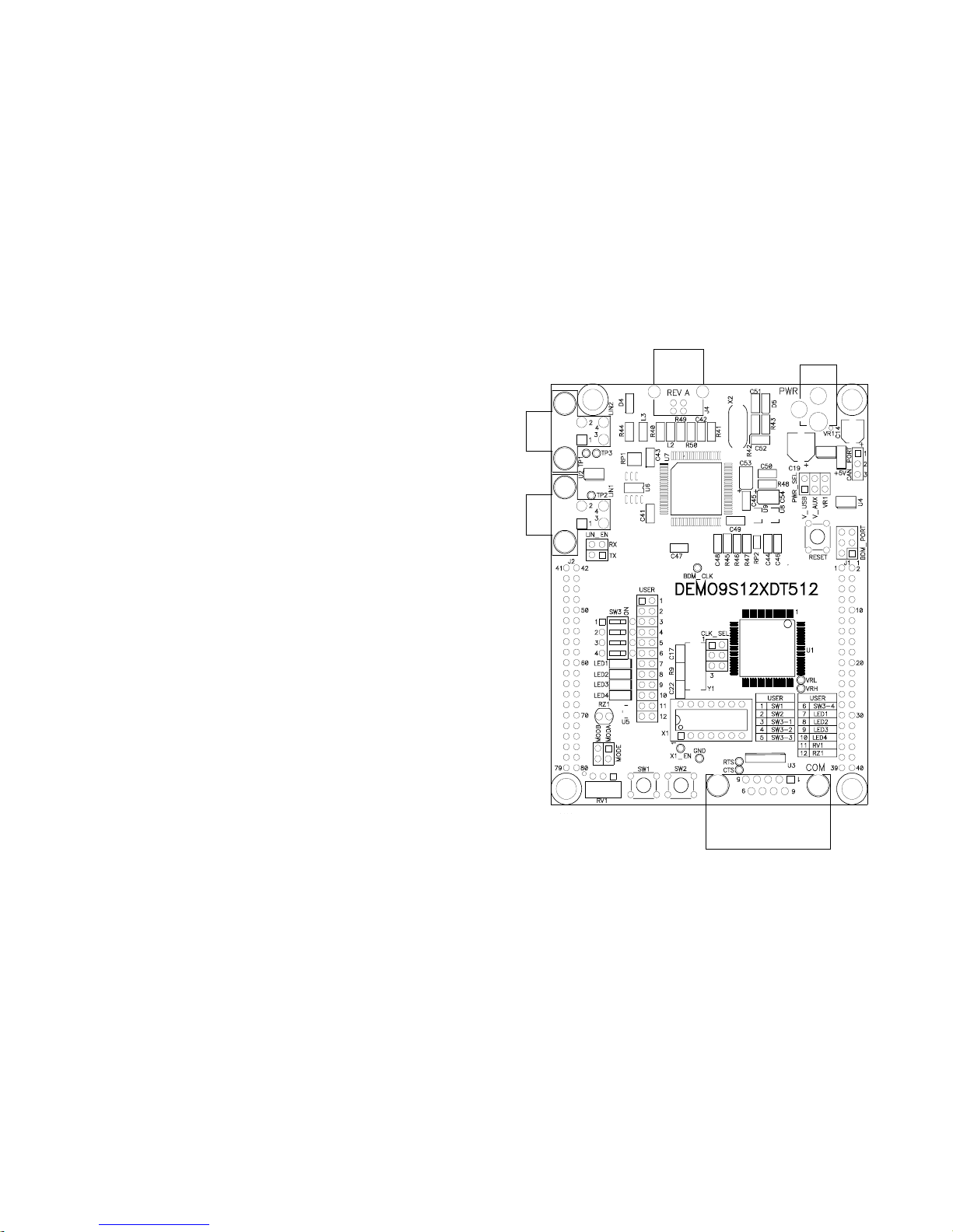
CONTENTS
CAUTIONARY NOTES ..............................................................................................................4
TERMINOLOGY.........................................................................................................................4
FEATURES................................................................................................................................5
REFERENCES...........................................................................................................................6
GETTING STARTED..................................................................................................................6
OPERATING MODES................................................................................................................6
RUN MODE........................................................................................................................... 7
DEBUG MODE......................................................................................................................7
MEMORY MAP ..........................................................................................................................8
SOFTWARE DEVELOPMENT...................................................................................................8
DEVELOPMENT SUPPORT......................................................................................................9
INTEGRATED BDM .............................................................................................................. 9
BDM_PORT HEADER........................................................................................................... 9
POWER....................................................................................................................................10
POWER SELECT................................................................................................................ 10
PWR_SEL........................................................................................................................10
VX_EN..............................................................................................................................11
RESET SWITCH ......................................................................................................................11
LOW VOLTAGE RESET..........................................................................................................11
TIMING.....................................................................................................................................11
COMMUNICATIONS................................................................................................................12
RS-232 ................................................................................................................................ 12
COM CONNECTOR.........................................................................................................13
LIN COMMUNICATIONS..................................................................................................... 13
LIN_EN.............................................................................................................................13
CAN COMMUNICATIONS................................................................................................... 14
MODE.......................................................................................................................................14
VRH/VRL..................................................................................................................................14
USER I/O..................................................................................................................................15
SWITCHES ......................................................................................................................15
LED’S...............................................................................................................................15
POT..................................................................................................................................16
LIGHT SENSOR...............................................................................................................16
USER SIGNALS.................................................................................................................. 16
USER ENABLE ................................................................................................................... 16
MCU I/O PORT.........................................................................................................................17
APPENDIX A............................................................................................................................19