BCF Technology OVISCAN 6 User manual

Page - 1
BCF TECHNOLOGY LTD
OVISCAN 6 + DUOSCAN 3
TECHNICAL MANUAL
Copyright BCF 2006
All rights reserved. Reproduction in whole or part of all material in this publication, including
drawings or diagrams is forbidden.
This manual is confidential to BCF Technology Ltd. and is supplied for use only in connection
with the operation and/or maintenance of the OVISCAN 6 as supplied by BCF Technology Ltd.
The contents must not be used for any other purposes, nor disclosed to any third party, without
prior consent of BCF Technology Ltd.
This document contains information available at the time publication. BCF Technology Ltd.
reserves the right to modify or revise its contents.

Page - 2
INTRODUCTION
This manual is intended to supplement the operators manual for the BCF OVISCAN 6 giving
more detailed technical information about the instrument and the data necessary to carry out
servicing and repair procedures.
Full information is given for the control console and module with some information being
supplied for the probes.
EQUIPMENT WARRANTY
The OVISCAN 6, including accessories is warranted against defects in design, materials or
workmanship, for a period of 12 months, from the date of commencement of the warranty period.
If any defect in design, material, or workmanship appears within the period of warranty, BCF
Technology Ltd. or its designated agent will in the case of all equipment, correct the defect by
making any necessary repairs or at its option, replacing any defective parts.
This warranty does not apply to and the company assumes no responsibility for damage or
deterioration due to any cause other than that specified above and in particular, but not by way of
limitation, this warranty does not apply to and the company assumes no responsibility for normal
wear and tear, or for damage or deterioration if the equipment has been subject to abnormal
conditions.
EQUIPMENT SERVICING
BCF Technology's products are supported by a world-wide network of highly trained technical
service representatives and engineers for prompt service of customer needs.
If required, rapid service assistance can be provided by contacting your local BCF Technology
representative, or communicating directly to:
BCF Technology Ltd.
3 Rutherford Square
Brucefield Industrial Park
Livingston
West Lothian
EH54 9BU
TEL: 44 (0) 1506 460023
FAX: 44 (0) 1506 460045
Email: office@bcftechnology.co.uk

Page - 3
CONTENTS
2DESCRIPTION AND OPERATION 4
Probe and Ultrasound Energy 4
OVISCAN 6 6
Overview 6
Console 6
CIRCUIT DESCRIPTION : Console PCB 9
Module 13
CIRCUIT DESCRIPTION : System PCB 15
CIRCUIT DESCRIPTION : Supply PCB 19
CIRCUIT DESCRIPTION : Interface PCB 21
MECHANICAL DISASSEMBLY 24
CONSOLE 24
MODULE 24
ANNUAL MAINTENANCE 25
CIRCUIT DIAGRAMS, PCB TEST AND LAYOUT 27
Console 27
Console PCB 27
Module 27
System PCB 27
Interface PCB 27
Supply PCB 27
WIRING SCHEDULES 27
Console 27
Module 27
Keypanel 27
APPENDIX : CONSOLE PCB DIAGNOSTIC INFORMATION 28

Page - 4
Description and operation
Probe and Ultrasound Energy
The standard probe has four transducers mounted in a drum which rotates in silicone fluid.
Connection to the rotating transducers is via slip rings and brushes from which four coaxial
cables carry the transducer signals to the receiver board. Only one transducer is used at any one
time.
The transmitter pulse waveform is selected to give efficient transformation from electrical energy
to ultrasound and a reduction of reverberation energy. The initial pulse at the transducer is
negative with an amplitude between 25 V. and 200 V. depending on the transmit power selected.
The negative voltage is held for a time equal to half the natural resonance period of the transducer
then released for an equal period then re-applied for a further equal period.
The system normally operates with the transmitter pulse width at the natural resonant frequency
of the transducer crystals and with the receiver filters set to the same frequency.
The system can be operated at other than the natural frequency, controlled from the menu settings.
The silicone fluid acts both as a lubricant for bearing surfaces and as a coupling medium for the
transmission of ultrasound energy to and from the face of the transducers. Ultrasound energy of
the frequency used in the OVISCAN 6 is strongly absorbed in air and will travel only a few
millimeters through it.
When the probe is not in contact with an object a characteristic reverberation pattern is displayed
on the screen. This happens because of the very large difference in acoustic impedance between
the material of the probe window and the outside air resulting in a very strong echo from the face
of the window. As this is close to the transducer, energy reflects back and forth between the
window and the transducer. This continues until the energy is reduced to an insignificant level.
When the probe is held in contact with an object which readily conducts ultrasound the
reverberation pattern disappears as the sound continues straight through the window and into the
object. In the case of using an animal as a scanned subject a couplant must be used to exclude air
from between the probe and the subject and prevent reverberation.
Because of the small distances involved in the generation of the reverberation pattern any small
distortion in the window can appear as a large distortion in the pattern. These distortions too will
disappear when the probe contacts a subject. Distortions in the window may occur as a result of
manufacturing tolerances or as a result of accidental damage to the probe.
For a similar reason, small differences in angular alignment between the transducers may appear

Page - 5
as a "flicker" in the reverberation pattern when the probe is not in contact with a subject. This
effect which shows a small random variation from probe to probe will also disappear when the
probe is scanning normally in contact with a subject.
The probe head also contains the following:
A dc motor and gear train to rotate the transducer drum.
A magnetic pick up, the resolver, sensing teeth on one of the gears to provide a signal for
rotational speed control and drum position feedback.
A magnetic pick up, the index sensor, sensing a slot cut into one of the gears providing a
signal to align the screen image with the transmitted sound.
A magnetic coupling to transmit the rotating forces through to the sealed compartment
containing the transducer drum.
A capillary tube to accommodate normal expansion and contraction of the volume of
silicone fluid without pressure changes.

Page - 6
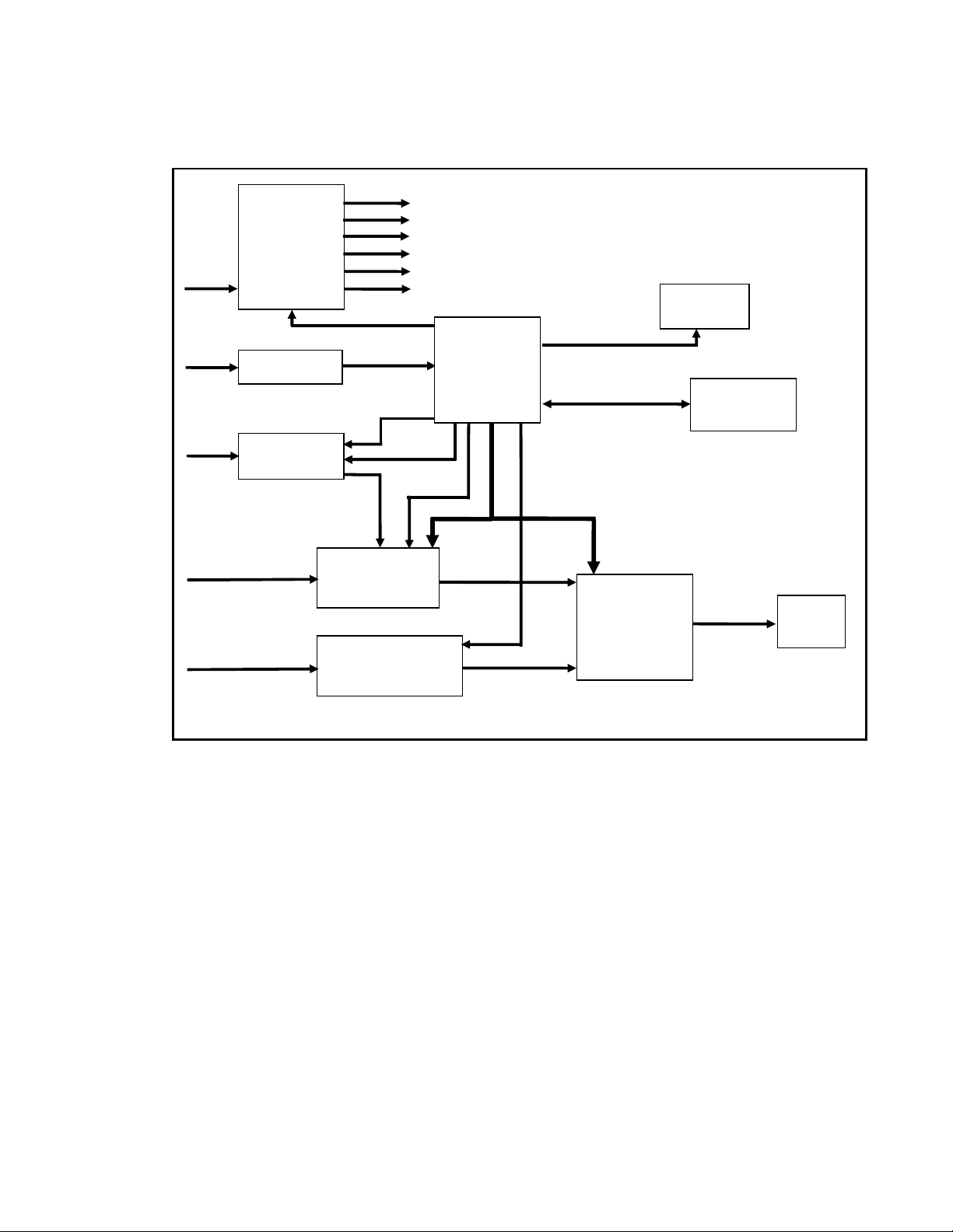
OVISCAN 6
Overview
The CONSOLE provides the display and interface to tally, drafting gate, RFID reader and video
monitor while the slide-in MODULE provides the ultrasound function.
Connection to and from the module is through the securing latches which provide power to the
MODULE and 5 blind mating contacts which provide serial communication and pass video
signals between the CONSOLE and MODULE.
The module can produce an ultrasound scan as a stand-alone
unit when latched to a battery and a
portable display connected.
The console can also function as a stand-alone video monitor in the absence of a Duo-Scan.
Console
Console components are built
into an inner chassis which
slides into the outer case. This
provides good environmental
and electromagnetic protection
for system components. Further
protection is provided by a
protective carry case. The
system is resistant to dust,
vibration and water splash.
DISPLAY
The LCD display normally
displays the Ultrasound image
CONSOLE
PCB
DISPLAY
MODULE
CONSOLE
PROBE
DC
POWER
TALLY
Drafting
O/P
Video Out
Video In
CONSOLE
PCB
DISPLAY
DC Power
Tally
Drafting
O/P
Video Out
Video In Rear
Panel
Front
Panel
Blind Mate
Connectors
From module
Serial Link
Digital Video
Serial
Link
Rear
Panel
RFID
Display

Page - 7
using digital Video output fed from the module to the console PCB via the blind mating contacts
at the rear of the module. The video is a proprietary digital format, this is converted into a VGA
signal for display on the LCD panel.
The LCD can alternatively be used in Video Monitor Mode to display NTSC analogue video
input from either the console rear panel video input connector or from the internal RF Video
receiver. Analogue video inputs are converted into a VGA signal.
CONNECTIONS
The rear panel provides connectors for DC power in (2 pin Binder), video in & video out (BNC)
and Drafting Gate output (5 pin Binder). The front panel connector is for the tally controller (6
pin Binder).
CONTROLS
The only direct input control to the console is the Tally handpiece which is used to power the
console on and select one of three video sources when the console is not connected to a Duo-scan.
When connected to a Duoscan power-on commands and any setup information is transferred to
the console via the serial link. Tally keypresses are handled by the console PCB which then
transfers the information to the module via the serial link.
POWER
The Console is powered with 12V DC via the 2 pin connector on the rear panel. The 12V DC
input is distributed to;
The Module, wired to the latches on the side of the Console through a 2.5A polyfuse.
The Console PCB. Circuitry has a 2.5A polyfuse and is reverse polarity protected.
The drafting gate output (via the Console PCB) with separate 2.5A polyfuse.
Once power is applied to the console PCB it remains in a low power standby mode, waking
briefly every second to check for serial data or tally command to power on in scanner mode or
video monitor mode.
VIDEO SWITCHING
If the console is powered without the Duo-Scan module present, pressing keys 1,2 or 3 on tally
handpiece switches the console on in video monitor mode. In this mode, the tally switches
between different video inputs; tally 1 switches to the Video Input BNC on the rear panel, tally 2
switches to the RF video receiver on the console PCB, each subsequent press of tally 2 cycles
through the 4 RF channels, tally 3 selects the Digital Video Input on the blind mating connectors.
Tally 0 returns the console into low-power, standby mode.
POWER ON SEQUENCE
Following power on, the Console runs through the following sequence:
1) Checks the supply voltage, if less than 9 volts then the console will display a “Low Battery”
message for approximately 6 seconds before switching into standby.
2) Configures its on board peripherals and switches to standby mode (LED 2 illuminates briefly).
WAKEUP SEQUENCE
On waking from Standby, the Console performs the following operations:
1) Checks the supply voltage, if less than 9 volts then the console will display a “Low Battery”
message for approximately 6 seconds before switching into standby.
2) Configures its on board peripherals and displays ‘Software OK’ message

Page - 8
3) Establish communications with the Duo-Scan module, if the appropriate response is received,
the console displays a “Duo Scan OK” message and goes into Duo-Scan mode. If no (or an
incorrect) response is received, the Console displays “Check Duo Comms” and switches into
Video Monitor mode, defaulting to the digital video input.
OPERATION (DUO-SCAN MODE)
During normal operation the Console runs through the following sequence in a repeating loop.
1) Check battery voltage if less than 9 volts then the console will display a “Low Battery”
message for approximately 6 seconds before switching into standby.
2) Poll Tally input to see if a button has been pressed.
If a button is pressed, the appropriate value is sent to the Duo-Scan module and the console waits
for a reply.
If the correct reply is received, the console continues with the normal sequence.
If no (or incorrect) reply is received, the Console displays “Check Duo Comms” and switches into
Video Monitor mode, defaulting to the digital video input.
3) Poll Duo-Scan serial link for any received data, if any commands are received, the Console
executes the appropriate routine: Brightness/Contrast, Drafting Gate setup, Power Off and the
store Brightness/Contrast commands.
OPERATION (VIDEO MONITOR MODE)
In Video Monitor Mode, the console polls the Tally input to check for button presses, the buttons
have the following effects:
Tally 1: Console displays “External Video” and switches to the Video In BNC on the rear panel.
Tally 2: Console displays “RF Channel X” where X is the currently selected RF video channel,
each press of the button cycles through the 4 available channels.
Tally 3: Console displays “Duo Scan Video” and switches to the Digital Video input on the blind
mate connectors.
Tally 0: Console switches into standby mode.
OPERATION (STANDBY MODE)
In Standby mode, the Console goes into a low power ‘sleep’ mode, it wakes up every second and
performs the following checks:
1) Check battery voltage, if the console entered standby due to a low battery, the console will not
power up unless the voltage is more than 11V, otherwise the battery voltage has to be above 10V.
2) Poll Duo-Scan Serial link, if any data has been received, the console will exit standby and
perform the Power On sequence.
3) Poll Tally, if any button on the tally controller is pressed, the console will exit standby and
perform the Power On sequence.
Page - 9
CIRCUIT DESCRIPTION : Console PCB
The Console PCB provides tally inputs, drafting outputs, communication with the Duo-Scan
module, video decoding and display signals and power. The 68HC processor (U2) is in overall
control of the operation of the Console PCB with the ability to disable parts of the circuit, as well
as shutting off power to all components except the tally pullups and RS232 transceiver (U7).
The processor reads the tally data, switches the drafting gate outputs, provides serial
communications with the Duo-Scan and the RFID reader and selects which of the 3 video inputs
is to be decoded and displayed.
POWER SUPPLY
The power supply section of the Console PCB provides power to all of the devices on the PCB
and to the inverter board for the LCD display.
The following supplies are generated:
Parallel
Video Data
Parallel
Video Data
Serial Links
Duo-Scan & RFID
Enable
I
2
C
Received Video
Drafting Outputs
Channel Select
Enable
Enable
Tally Inputs
Power On
Power Supply
Tally Pullups
RF Video Rx
U3
Video Decoder
U1
LVDS De-serialiser
Drafting
Output
RS232
Interfaces
U6
EP1C3T100C6
FPGA
12Vdc
Tally
Input
Aerial
Video In
Digital Video In
SK2
Display
1.5Vdc
1.8Vdc
3.3Vdc Standby
3.3Vdc (a)
3.3Vdc (d)
5Vdc
Block Diagram
U2
68HC908AP8
Processor

Page - 10
3.3Vdc Standby – Supplied by linear regulator, U13, to the processor, U2, RS232 transceiver, U7,
and tally inputs pull ups (RN1 & RN2). This supply is permanent and cannot be switched off, so
that the processor remains powered in standby mode and can detect tally inputs or serial data.
12Vdc – Supplied by switching regulator, U5, to the LCD Display inverter board and to the other
voltage regulators (except the 3.3Vdc standby). This supply is under processor control via the
‘Power on’ line (U2 pin 42 to U5 pin 6, active high). Disabling this supply also disables the other
supplies, placing the Console in Standby mode. U5 is a Buck/Boost switching regulator which
will generate regulated 12Vdc from a supply voltage of 9-18Vdc. External switching components
M5-M8 are used in pairs according to whether the input voltage is above or below 12V; in step up
mode, M5 is on, M6 is off and M7 & M8 are switched. In step down mode, M7 is on, M8 is off
and M5 & M6 are switched. R26 provides current feedback to the device.
5Vdc – Supplied by switching regulator, U10, to the Airwave RF video receiver (RX2) and the
video amplifier U11 via the linear regulator (U14).
The switching regulator steps down the 12 supply from U5 to 5.35Vdc, this is fed to linear
regulator U14 which supplies a regulated 5Vdc supply to the RF video receiver. The output from
U14 may be disabled by the processor via the ‘Vid RX On” line (U2 pin 37 to U14 pin 7
Enable=High).
3.3Vdc – Supplied by switching regulator, U9, split into 2 supplies, 3.3VD and 3.3VA (digital
and analogue) separated by filters. This regulator also supplies power to the 1.8 & 1.5V supplies.
The 3.3VD supplies the analogue video converter and LVDS De-serialiser (U3 & U1), the crystal
for the dgital video converter (X2) and the FPGA (U6).
The 3.3VA supplies the digital video converter (U1).
1.8Vdc – Supplied by linear regulator, U12, this regulator is powered by the 3.3Vdc supply.
The 1.8Vdc supplies the analogue video decoder (U3).
1.5Vdc - Supplied by linear regulator, U4, this regulator is powered by the 3.3Vdc supply.
The 1.5Vdc supplies the FPGA (U6).
Video Processing
Analogue video inputs:
The Console PCB accepts analogue video from 2 sources; RF, via the Airwave receiver and
composite via the Molex connector J11.
RF Video: The Airwave receiver (RX2) receives RF video via the aerial connected to PCB, the
receiver has 4 input selection lines (RF_SEL_0 to RF_SEL_3 all active low) which are controlled
by the processor, U2, to select the desired channel. The power supply to the receiver (5Vdc) can
be disabled by the processor, switching off the receiver.
The selected channel is fed to the External Video Out connector (J10) via the video amplifier U11
and to Input A (pin 1) of the Analogue Video Decoder.
External Video: The external video input is fed to connector J11 and from there to input B (pin
2) of the Analogue Video Decoder.
Analogue video decoding:
The Analogue Video Decoder (U3) has 2 video inputs (A & B) which are connected to the RF

Page - 11
video receiver output and the external video input respectively. Control over which input is
decoded is via the I
2
C bus from the processor. The decoder also has a single output (under I
2
C
control) which is used to drive an LED (LD2), illuminated by the processor when the decoder is
active.
The selected input is converted to a digital video signal to ITU-R BT.656 standards and fed to the
FPGA (U6) via 8 data lines and 1 clock line.
The analogue decoder is powered by the 3.3V power supply and as such is shut down when the
processor disables supplies in standby mode, the device also has a separate enable line
(Vid_Comp_On) which is under direct processor control (U3 pin 28 to U2 pin 41 active high).
When the device is active there should be data on all 8 lines and a clock on the clock line.
Digital video input and decoding:
The Console PCB accepts a single serial digital video source via the blind mate connectors in the
console to Molex connector J4.
This signal is a differential serial signal using a proprietary video format, the LVDS De-Serialiser
converts this signal into a 10-bit parallel signal, this is fed to the FPGA over 10 data lines and 1
clock line.
The de-serialiser is powered by the 3.3V power supply and as such is shut down when the
processor is in standby mode, the device also has a separate enable line (LVDS_On) which is
under direct processor control (U1 pin 7 to U2 pin 17 active high).
The ‘Lock’ output of the device is connect to an LED (LD4), this illuminates when the device has
locked onto a valid serial data stream.
Video Conversion and display driver.
The parallel digital video signals from the analogue video decoder and the deserialiser are fed to
the FPGA, in addition, the FPGA has its own internal video source which is used to display the
various system text messages. The appropriate source is selected by the processor via the I
2
C bus.
The output is a 18 bit RGB digital video signal (6 bits per channel) with separate horiziontal and
vertical syncs and clock. In operation, there should be data present on the data lines (R0-R5, G0-
G5 & B0-B5) as well as on the sync and clock lines.
When the FPGA is displaying its internal source (text messages), LED LD1 is illuminated.
Interfacing and processing
The processor (U2) controls the overall operation of the console, controlling the power supply to
the other devices and display and handling the serial interfaces, tally input and drafting output
switching.
The processor is attached to an LED (LD3) which is illuminated following processor
configuration.
Serial Interfaces:
The processor provides 2 serial interfaces, both are configured at 9600 baud, 8bits, 1 stop bit, no
parity. Both interfaces are routed from the processor to an RS232 Transceiver (U7) and from
there to connectors J6 & J7. Connector J6 connects to the blind mate connectors on the console
to provide communications with the Duo-Scan, J7 connects to the rear panel 9 way D-type
connector for communications with the RFID reader.
Tally input:

Page - 12
The front panel tally connector on the console connects to J5 on the PCB, providing 4 discrete
input lines for the tally input. Each line is pulled high by resistor RN2 and is pulled low when the
appropriate tally button is pressed. These 4 lines are read by the processor (on pins 19-22) which
then transfers the tally data to the Duo-Scan over the serial link.
If the processor receives the correct response from the Duo-Scan, it then switches the appropriate
drafting outputs, if not or if an incorrect response is received from the Duo-scan, the console
switches into Video Monitor Mode.
Drafting Output:
The console provides 4 drafting outputs and a 12Vdc supply line via the 5 pin Binder connector
on the rear panel connected to J8 on the Console PCB. The 12Vdc output is unregulated 12
supply (9-18Vdc) fused with a 2.5A polyfuse.
Each output line is switched via a FET (M1 – M4 for Draft-1 to Draft-4 respectively). To switch
the output on, the processor applies a logic 1 to its output, switching on the appropriate FET, this
pulls the drafting output to 0vdc, completing the circuit.
Page - 13
Module
The module forms a self
contained scanner with basic
functions and preset controls.
Connections for probe and
display are on the front panel. DC
Power is supplied to the module
through its latches.
Mounting in the Oviscan console
connects I/O through the blind
mate connector on the rear panel,
providing further controls and
video output.
POWER
The DC power in from the latches is protected from reverse polarity and overcurrent by Diode
and polyfuse. A High-Side switch IC (U105) Passes power to the Supply PCB under control of a
logic level input. This power-on control line can be driven by one of three sources; the System
PCB under Microprocessor control, the front panel ‘POWER’ key, or shorting link (J100) on
Supply PCB.
Pressing the keypanel power switch powers up the system; once the System Board Core is loaded
successfully the power switch control line is latched on and the front panel indicator is lit (Key
can be released after a few 100uS). The ‘POWER’ key is also read as an input to the System
Core, enabling detection of a long press (>2sec) to toggle power off.
The Power switch IC provides current limiting and is overload protected.
DISPLAY
Output connector provides +6.5V, +12V supplies and Video composite greyscale signal (with
NTSC timing).
PROBE
15 Way mixed coaxial and pin connector carries co-axial signals to/from the four transducers,
probe resolver and index signals, motor drive and identifier resistor.
Single pins are used for image wobble correction potentiometer connections and grounding.
KEYPANEL
The five keys are read by the System core and used to control all settings through a menu system.
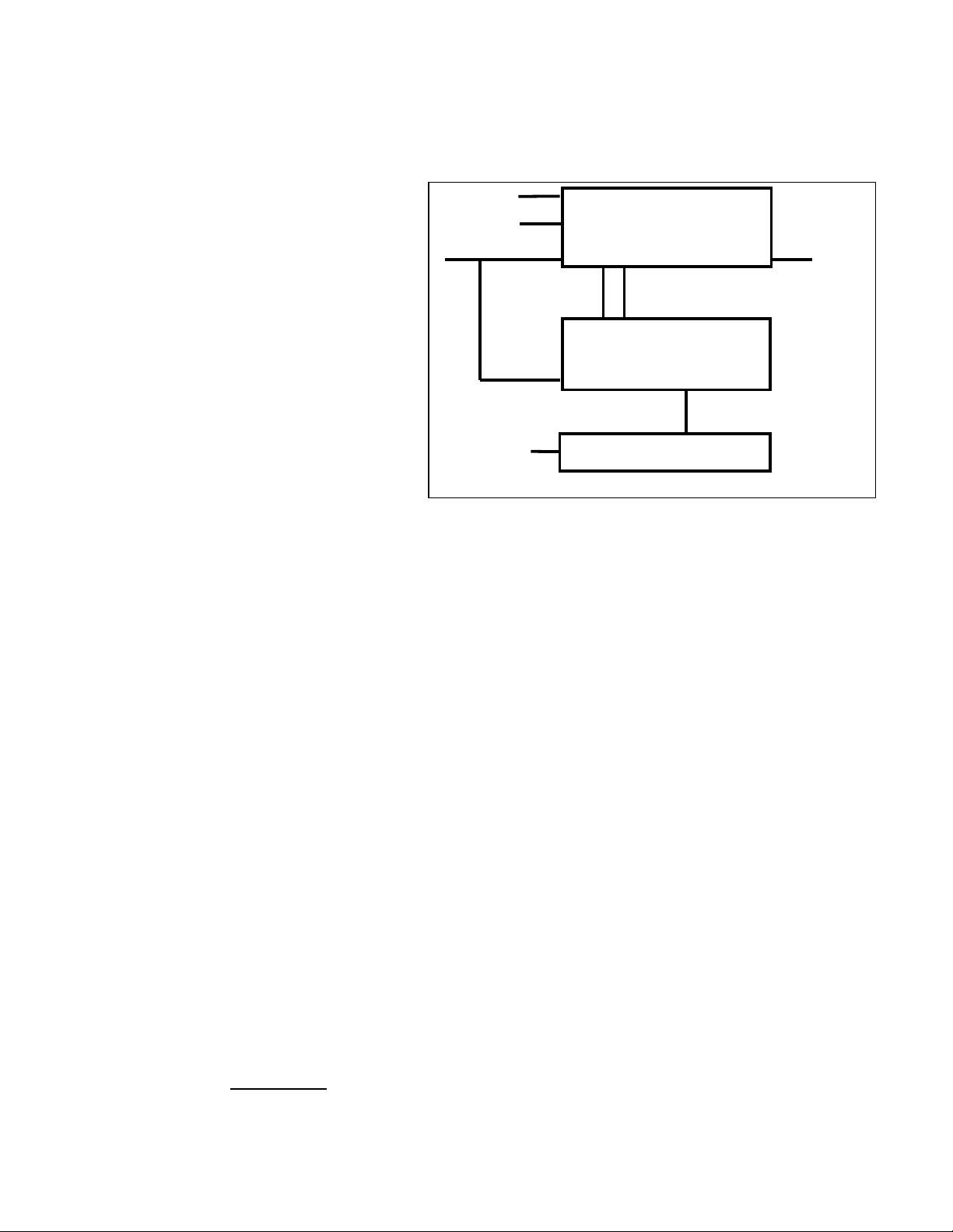
CIRCUIT BOARDS
The module consists three PCBs:
•The Supply Board switches the incoming DC supply and provides all DC supplies for the
display connector and PCBs including variable high voltage supply for the TX transmitter. In
INTERFACE PCB
SUPPLY PCB
SYSTEM BOARD
PROBE
DISPLAY
12V DC
2 x 20 way ribbon cable
20 way ribbon cable
Transducers
Wobbles
Identifier
Motor
Index
Resolver
KEYPANEL
BLIND MATE
CONNECTOR
Video + Serial

Page - 14
addition there is an A-to-D converter reading DC input voltage, and drive to front panel
LED.
•The System board combines Analogue Ultrasound functions (Crystal selection, Ultrasound
transmit, Ultrasound receive processing and sampling) with scanner control and digital
processing functions (Ultrasound digital processing, Scan conversion, Graphics generation
and serial Digital video output, Probe control, scanner setup through control menu.
•The Interface board reads keypanel inputs, digitizes probe index, resolver, wobbles and
identifier, sending digital values to the System Board. Video data from the System board is
converted to composite video analogue signal to front panel and to PCB-mounted video
transmitter module. The Interface board also generates the motor drive voltage under System
board control.
SERVICE MENU
A service mode can be entered on the Duoscan enabling test routines and other data display. It
can be used to display Index and resolver waveforms, and a total of all Tally batches that have
been cleared.
To enter service mode, with the Duoscan connected to a console, press keypanel button 1 to scroll
through to the ‘foetal age’ menu. With foetal age selection ‘OFF’ Press and hold buttons 3&4
until ‘service’ menu appears. Press button 4 to scroll through the series of tests or press button 3
to toggle between Total tally display and live display of digitized values of probe identifier and
wobble correction pots. To exit service mode, remove power from the scanner.
INDEX, RESOLVER DISPLAY
Index and resolver waveforms may be displayed on-screen when the Duoscan is connected to a
Console and a probe connected. Enter service mode and press button 4 to scroll through to test 1
or 2 (1 or 2 displayed in TALLY LATE column) for Index or Resolver display. In either of these
two tests, an analogue version of the on-screen displayed values is provided on the video out
connector in place of NTSC video signal.

Page - 15
CIRCUIT DESCRIPTION : System PCB
TRANSDUCER SELECTION
The ultrasound is generated by pulsing the transducers in the probe. There may be either two or
four transducers fitted to the probe; only one pair of transducers is used for any one imaging
mode. From the selected pair of transducers only one is used at a time, with alternate transducers
used on consecutive image frames . When a mode is selected the desired pair of transducers is
connected to two separate transmit\input selection circuits selected by latching relay RL100
(DPCO). The relay has two coils, one to switch into each state. The coil is energized by a short
pulse (few 100mS) when a change of selection is required, generated by core IC, buffered by U9
and driven by high side switch (M103 or M106) from the 6.5V supply. As alternate ultrasound
frames are displayed, the appropriate transmitter is used and only one of the two input selection
circuits is enabled.
TRANSMITTER
The Transmit pulse timing is generated digitally (Core IC) and fed through buffer U9 to one of
two transmitters. Capacitatively coupled transistor Q100 acts as a current source to drive the gate
of power FET M1. Transistor Q101 provides gate voltage clamping for M1 and gate discharge for
fast turnoff of M1. The Large negative transmit pulse is coupled to the selected transducer
through diode D8. When not transmitting, D8 is biased off to isolate transmitter noise from the
received signal path.
PROTECTION\SELECTION
Each of the two active transducers connects to a protection\selection circuit. Only one of the two
TRANSDUCER
SELECTION
RL100
INPUT SELECT
+PROTECTION
D5,D6,M100
VGA
U2
ANTI-
ALIAS
FILTER
L2,L3,C6
A
TO
D
U5
SYSTEM CORE CPLD U4
GAIN CONTROL
U11
P
R
O
B
E
I
N
T
E
R
F
A
C
E
TRANSMITTER
PULSER M1
INPUT SELECT
+PROTECTION
D1,D2,M101
TRANSMITTER
PULSER M2
S
U
P
P
L
Y
SERIALIZER
GRAPHICS
CONTROL
PROCESSOR
PROCESS
U
-
SOUND
MEMORY
(SRAM)
U8
BOOT
MEMORY
(FLASH)
U10
SCAN
CONVERT
TX VOLTS+
V DC SAMP
IIC BUS
DC
SUPPLIES
DIGITAL
VIDEO
POWER
CONTROL
TIMING
INDEX,
RESOLVER
IIC BUS
MOTOR
IDENTIFIER
WOBBLES
IIC BUS
CRYSTAL
OSCILLATOR

Page - 16
selection circuits is enabled by biasing the diode protection circuit on; Core IC, Level translate
M105,M107, high side switch M100,M101. The unbiased circuit does not pass any small signal;
D6, D5 do not conduct while the signal is less than +/- 0.5V. The selected diode protection circuit
which is biased on passes small signals through D1,D2 but blocks any large (transmit) pulses.
RECEIVE PROCESSING
The small received echoes from the selected input are passed through lowpass filter L6, C13 and
are amplified by U2. U2 is a variable gain amplifier with low noise preamplifier. The gain of the
preamplifier and input impedance are set by feedback resistors R7, R8. The variable gain stage
provides from -12dB to +36dB with a differential output. A ramp voltage between 0 and 1V
generated by digital potentiometer U11 under core IC control varies the gain setting. L2, L3, C6
form a 2-pole anti-alias filter before coupling to the analogue-to-digital converter U5 through TF1
which provides dc level isolation between U2 output bias level of 2.5V and U5 input bias below
1V.
SAMPLING
U5 is a high-speed sigma-delta A-to-D converter with onboard DSP and clock generation
providing a 14-bit output at 30 MHz and 80dB anti-alias filtering with a 2V p-p differential input.
U5 is reset following power up and configured over SPI bus by the core IC. Parallel data is passed
directly to the core IC. U5 requires a 1.2V supply filtered separately for analogue and digital
internal functions, and a 2.1V supply for its output pin drive.
CORE FUNCTIONS
Internal to the Core IC, the digitized ultrasound is operated on by means of digital signal
processing to provide filtering, compression, automatic Gain Control, and brightness mapping.
The internal scan converter writes the processed ultrasound value and its corresponding screen
location address to the graphics memory. The graphics generator reads the data back to produce
both encoded VGA and composite NTSC timed digital video outputs. The encoded VGA digital
video signal is passed to an on-board parallel to serial LVDS driver chip. Digital NTSC video
data is passed to the interface PCB.
The probe index and resolver pulses are digitized on the Interface PCB along with Wobble
correction pot settings and processed in the System core using a digital PLL to generate the digital
frame and vector pulses related to precise crystal position with wobble correction, and used for
the scan converter timing within the core. The drum position is decoded to select between the two
transducers currently being used for imaging, appropriate input source and transmitter being
selected. U4 runs on a 1.2V supply (with separate filtered feeds to internal PLLs), a 2.1V supply
is used for interface to A\D converter connected (all pins 56 to 104) and a 3.3V supply is used for
all other input\output pins.
CONTROL
Within the core IC is a processor which is responsible for system configuration and user interface
(information display and menu) with access to display memory, probe identifier digital value and
keypanel data fed from the interface PCB. The resolver period is also monitored by the processor

Page - 17
to adjust the probe rotation motor speed, controlled over IIC Control bus to the Interface board
which generates the motor drive DC voltage. The transmitter supply voltage on the supply PCB
can be varied and the incoming 12V supply voltage can be monitored over the supply IIC bus.
Control can be switched over to an alternate pair of crystals by a latching relay, for example if a
dual-frequency probe is used.
MEMORY
All non-volatile data is stored in U10 serial Flash device. The three main sections are Firmware
configuration data, Software, and System stored values (Running tally, overall tally, preferred
startup mode, duoscan modes) System storage area can be read and re-written by the processor
within the core IC.
IC U8 is 2Mx8bit SRAM. It is used as display memory for the 640x480 display area which can
be written to by firmware and read or written by core processor. The remaining area is used for
software storage.
FIRMWARE STARTUP
These steps are followed during system initialization on power-up:
core CPLD senses power-up and loads configuration data from serial flash Boot ROM device
U10 to configure the CPLD firmware including the processor.
Successfully configured processor within CPLD logic transfers software program from boot ROM
to SRAM.
Processor resets and runs from SRAM program and initializes the system as follows;
SOFTWARE STARTUP
Short delay (prevents accidental switch on) followed by core driving power enable line.
Sets up SPI for comms with flash memory.
First beep.
Sends ASCII data at low baud rate to wake up console.
Sends ASCII ‘H’ character at 9600 baud to establish console comms.
Sets motor speed to the lowest value.
Reads ‘Total Tally’ configuration byte from Flash, if the value is incorrect, the flash is then
initialised. If the value is correct, the system calculates the total tally.
Reads ‘Running Tally’ configuration byte from Flash, if the value is incorrect, the flash is then
initialised. If the value is correct, the system calculates the running tally.
Switches front panel LED on.
Reads Duo_Mode 1 and configures Range, Frequency etc.
Writes menu data to display.
Configures Index /Resolver A/D.
Sets output power.
Sets motor speed.
Enable Index/Resolver sampling.
Enable Ultrasound scan.
Second Beep.
Enters mains loop.

Page - 18
N.B. Once in the main loop, the Duo-Scan will poll the RS232, if it receives an ‘H’ character
from the console, it undergoes the following process:
Read Drafting Data from console.
Read Brightness & Contrast values from Console.
Read Ovi-Scan mode data from flash.
Setup Range, Frequency etc.
Write Ovi-Mode menu to display.
Once the system has initialized, the controller continually monitors the probe identifier for
change, interrupted only by a keypress.

Page - 19
CIRCUIT DESCRIPTION : Supply PCB
SUPPLY
BOARD
The Supply board accepts an input voltage range of 9 to 18 V and generates all system supplies
required, passing them to the SYSTEM board through a 20 Way ribbon cable
Input protection
The input supply is connected to the supply board through flying lead to CN1. Reverse polarity
and overcurrent protection is provided by polyfuse F1 with trip current of approx. 2.5A. This
device automatically resets following removal of fault condition, when it cools down. Diode
D101 shorts a wrong polarity supply through F1, causing it to trip and limiting reversed circuit
supply to less than 1V.
Soft Switch
The incoming supply is switched by U101 which is a high-side FET with internal overcurrent and
overvoltage protection. When power is first applied the ‘POWER ON’control line is biased to
3.3V by pullup resistor R121, switching M100 on and pulling pin2 of U101 low (switch is OFF).
The ‘POWER ON’ control line can be pulled low by the system board or by link J100. M100 is
switched off and pin2 of U101 is pulled high by R127 (switch is ON). Switched, fused input
voltage is routed to the rest of the supply board and to the front panel display connector
Supply Bus; 6.5V
Switched, fused input supply feeds a high efficiency ISRs Integrated Switching Regulator SR1.
Similar to a DC-DC converter, except the output supply is not isolated from the input. The
converter has overload protection and can supply up to 2A.
The 6.5V bus feeds the two IC based converters which step down to 2.1V and 3.3V and is passed
to the supply board for further distribution and regulation. It also supplies the front panel display
connector via filter based around L103 and J101.
INPUT
PROTECTION
6.5V BUS
CONVERTE
2.1V
SWITCHE
3.3V
SWITCHE
- HT SUPPLY
GENERATION
1.8V TO SYSTEM
6.5V TO DISPLAY CONN
3.3V TO SYSTEM
-
HT TO SYSTEM
LED DRIVE
Vin ROUTED TO
DISPLAY CONN
SOFT
SWITCH
CONTROL
FROM
SYSTEM
BOARD
ANALOGUE
SAMPLING
CONVERTER
IIC CONTROL BUS

Page - 20
Low Voltage switchers
Based around switching regulator chips MAX887 (U3, U12) with integrated switching FET, the
inductor and diode on the output are used to provide smoothed voltage across the output
capacitor. A resistor network from the output feeds back to the chip to provide regulation. Output
is short circuit protected. Further filtering is provided by inductors L104, L106 used to feed the
System board.
- HT Generation
A variable high voltage supply is generated by step-up switching regulator controller U102.
Current in the primary of the planar transformer flows from the 12V supply through M101 until
peak primary current is reached (U102 senses voltage rise across R118). M101 is switched off
and the collapsing magnetic field generates a high (negative) voltage across the secondary (1:10
turns ratio). D102,D104 rectify the high voltage which is then stored on C5. R1, R2,C114 provide
low pass filtering and limit the discharge current if the HT supply output pin is suddenly shorted.
The HT voltage is regulated by U102 which alters the transformer pulse frequency to maintain a
voltage of 1.2V at pin 3 (feedback) input. The negative high voltage output draws a small
feedback current through R136+ R138 proportional to the output voltage. This small current is
mirrored by transistor pair Q100, Q102, with R112 setting mirrored current 10x current in R111.
The voltage at the controller feedback pin is a function of this mirrored current (proportional to
output voltage) and the resistance from this pin to ground. The digitally controlled resistor U101
has a range from 0-10Kohm, giving an output voltage range from -25V to -200V. Q101 is wired
as a diode to limit possible high negative voltage across the current mirror. The switching
controller limits current in the transformer primary every cycle to prevent transformer saturation.
The limited switching frequency ensures output supply is current limited at about 7mA at -200V
with short circuit protection. Oscillations in the Switching circuit which could potentially
interfere at ultrasound frequencies are minimized by snubber components L101,C108. Variable
resistor U101 is controlled over the IIC bus from the system board.
DC input voltage sensing
The incoming DC supply voltage can be measured, and any step rise in the supply voltage due to
the input switch being briefly switched off can be measured. These voltage readings taken over
the IIC bus are used to calculate as accurately as possible the battery voltage while eliminating the
effect of voltage drop over the varying resistance of the battery connection latches. U103 is a 4-
channel 10bit A-to-D converter with an internal 2V reference. Ch1 reads any positive step
increase in the DC input voltage up to 2V (readings taken after the power switch IC is briefly
switched off), Channel 2 senses the switched input voltage scaled to read 0V to 22V, Channel 3 is
used to read a scaled version of the unswitched DC input voltage (0-22V), Channel 4 input is not
used.
This manual suits for next models
1
Table of contents
Other BCF Technology Scanner manuals


