BCM SQ574 User manual

SQ574 Pentium PCI
Mainboard
User’s Manual

SQ574
ii
User‘s Notice
Static Electricity Precaution
Static electricity can easily damage your SQ574 mainboard. Observing a few basic
precautions can help you safeguard against damage that could result in expensive repairs.
Follow the simple measures below to protect your equipment from static electricity damage:
Keep the mainboard and other system components in their anti-static packaging until you are
ready to install them.
Touch a grounded surface before you remove any system component from its protective anti-
static packaging. Unpacking and installation should be done on a grounded, anti-static mat.
The operator should be wearing an anti-static wristband, grounded at the same points as the
anti-static mat.
After removing the mainboard from its original packing, only place it on a grounded, anti-
static surface component side up. Immediately inspect the board for damage. Due to shifting
during shipping, it is suggested that the installer press down on all of the socket IC‘s to
ensure they are properly seated. Do this only with the board placed on a firm flat surface.
During configuration and installation, touch a grounded surface frequently to discharge any
static electrical charge that may have built up in your body. The best precaution is to wear a
grounded wrist strap. When handling the mainboard or an adapter card avoid touching its
components. Handle the mainboard and adapter cards either by the edges or by the adapter
card’s case mounting bracket.
The information presented in this publication has been carefully screened for reliability. The
manufacturer provides this manual “As is” with no warranties of any kind, either expressed
or implied, including but not limited to the implied warranties or conditions of this product’s
fitness for any particular purpose. In no event shall the manufacturer be liable for any loss of
profits, loss of business, loss of data, interruption of business, or indirect, special, incidental,
or consequential damages of any kind, even if the manufacturer has been advised of the
possibility of such damages arising from any defect or error in this manual or product.
The manufacturer has the right to change this specification without pre-notice.
Trademarks and product names appearing in this manual are may or may not be registered
with their respective holders.

SQ574 iii
Table of Contents
1INTRODUCTION......................................................................................1-1
1.1 OVERVIEW .............................................................................................1-1
1.2 HOW TO USE THIS MANUAL.....................................................................1-1
1.3 ITEM CHECKLIST ....................................................................................1-2
2KEY FEATURES.......................................................................................2-1
2.1 PRODUCT SPECIFICATION........................................................................2-1
2.2 MAINBOARD LAYOUT ............................................................................2-2
3INSTALLATION PREVIEW......................................................................3-1
3.1 INSTALLATION OF DRAM MODULES (SIMM OR DIMM)..........................3-1
3.2 INSTALLATION OF THE CPU ....................................................................3-4
3.3 INSTALLATION OF EXPANSION SLOTS:.....................................................3-5
3.4 INSTALLATION OF IDE, I/O CABLES CONNECTION....................................3-6
4BIOS SETUP..............................................................................................4-1
4.1 STARTING SETUP....................................................................................4-1
4.2 MAIN SETUP MENU ................................................................................4-3
4.3 STANDARD CMOS SETUP MENU.............................................................4-4
4.4 BIOS FEATURES SETUP MENU................................................................4-8
4.5 CHIPSET FEATURES SETUP MENU ..........................................................4-11
4.6 POWER MANAGEMENT SETUP MENU .....................................................4-13
4.7 PCI CONFIGURATION SETUP MENU.......................................................4-16
4.8 INTEGRATED PERIPHERALS MENU..........................................................4-18
4.9 IDE HDD AUTO DETECTION................................................................4-20
4.10 PASSWORD SETTING.............................................................................4-20


SQ574 1-1
1Introduction
1.1 Overview
The SQ574 mainboard integrates the Pentium microprocessor, memory, and I/O technologies
and is designed to fit into a standard AT form factor chassis. The design supports Pentium
processors, Pentium processors with MMX technology, Cyrix 6X86/6X86L/MXProcessors,
and AMD K5/K6 Processors, IDT-C6 Processors.Page 2-2 illustrates the mechanical form
factor for the SQ574 mainboard.
1.2 How to use this Manual
This manual provides information necessary to install and operate the SQ574 mainboard and
is organized into four chapters. The purpose of this manual is to explain the installation
procedures and operations of the mainboard as specified below.
1. Introduction Manual information and checklist
2. Key Features An overview specification of this mainboard
3. Installation Instructions on how to setup the mainboard
4. BIOS setup BIOS software setup information

SQ574
1-2
1.3 Item Checklist
The SQ574 mainboard should contain following items (ü). Immediately, contact your
retailer if you discover any missing items, or any damage.
þThe SQ574 mainboard
þThis SQ574 user‘s manual
þ1 IDE ribbon cable
þ1 floppy ribbon cable
þ1 parallel ribbbon cable attached to a mounting bracket
þ2 serial ribbbon cable attached to a mounting bracket
þDriver diskeete
q1 PS/2 cable with bracket (optional)
qUSB (2 port) cable with bracket (optional)
qInfrared (IrDA) module with ribbon cable (optional)

SQ574 2-1
2Key Features
2.1 Product Specification
²Processor: Supports 120-300MHz Intel Pentium Processors (P54C), Pentium
Processors with MMX Technology (P55C), AMD-K5, AMD-K6 and Cyrix 6X86,
6X86L, 6X86MX Processors, IDT-C6 Processors. The ZIF Socket 7 will support future
Pentium Overdrives.
²L2 Cache: Onboard 512KB Pipeline Burst SRAM
²SIMM (System Memory): Supports 70ns or faster Extended Data Output (EDO) or
Fast Page (FP) SIMM in four 72-pin SIMM sockets using 4MB, 8MB, 16MB, 32MB
or 64MB for a maximum of 256MB system memory.
²DIMM (System Memory):Supports 66MHz or faster unbuffer 2 or 4 clock 3.3V
DIMM in two 168-pin DIMM sockets using 8, 16, 32, 64 or 128 for a maximum of
256MB system memory.
²Chipset: Intel Triton 430TX set is the core chipset with an Winbond 977 super I/O
controller chip.
²Expansion Slots:Four 32-bit PCI and Three 16-bit ISA expansions slots (one
shared).
²Super Multi-I/O:Two high-speed UART compatible serial ports and One parallel
port with ECP and EPP compatibility. One FDD header supporting either 5.25“ or 3.5”
(1.2 or 1.44/2.88MB) floppy drives. One IrDA TX/RX infrared port.
²Keyboard and PS/2 Mouse: Onboard Standard AT Keyboard and PS/2 Mouse Port
²PCI bus Master IDE Controller:Onboard dual-channel PCI Bus Master IDE
support 4 IDE devices. This controller supports PIO Mode 3 and Mode 4 with a data
transfer rate up to 17MB per second. An Ultra DMA 33 (UDMA) supports data
transfer rates up to 33 MB per second. Also supports LS120 Floppy Drive.
²Universal Serial Bus (USB):Two standard USB interface supports up to 48MHz and
127 peripheral devices.
²PCI BIOS:Win 95 Plug and Play with Green power saving support, and DMI
Support.
²Mechanical: Baby AT form factor 220 mm x 252 mm
²Additional Feature: SB-LINK header to support legacy sound blaster compatible
audio to the PCI bus.
²Jumperless Design: Using the onboard BIOS, Jumpers settings are no longer needed.
SQ574
2-2
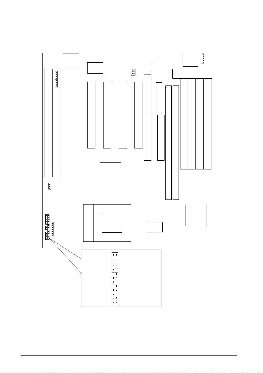
2.2 Mainboard Layout
P/S 2
Mouse
16-Bit ISA Slot
16-Bit ISA Slot
ISA Slot
32-Bit PCI Slot
32-Bit PCI Slot
32-Bit PCI Slot
32-Bit PCI Slot
Floppy Drive Conn.
Secondary IDE Conn.
Primary IDE Conn.
COM2
COM1 Power Input Conn.
KBD.
Conn.
DIMM Socket 1
SIMM Socket 1
SIMM Socket 2
SIMM Socket 3
SIMM Socket 4
PIIX4
MTXC
64Kx64 512KB
Pipline Burest Cache
Memory
16-Bit ISA Slot
ZIF Socket 7
Flash
BIOS W83977F/AF
SPEAKERKEYLOCK
ExternalSMI
TurboLED
RESET
SuspendLED
HDDLED
SUB-LINK
(J15)
Fan (JP17)

SQ574 3-1
3Installation Preview
Before you install the SQ574 mainboard into the system chassis you may find it convenient
to first configure the mainboard hardware. This section describes how to install memory
modules, and how to attach the various system components. Before using your computer you
must review the following 6 steps:
1. Installation of DRAM modules (SIMM or DIMM)
2. Installation of the CPU
3. Installation of expansion cards
4. Installation of IDE, I/O cables connection., and Power Supply connection
5. Installation of the Power Core to the System.
6. Setup of the system BIOS software
WARNING: When handling the system upgrade or plug in additional Add-On Card, please
be sure your System is Power Off.
3.1 Installation of DRAM modules (SIMM or DIMM)
3.1.1 SIMM (Single Inline Memory Module)
You can configure the system memory size in a variety of ways by using different
combinations of the four 72-pin DRAM SIMM. The memory must be 70ns (nanoseconds) or
faster using either Fast Page Mode or Extended Data Output (EDO) types. The memory
table below shows the different memory size combinations available. Please pay attention to
the following restrictions :
1) You must use one pair of sockets at a time in sequence ( i.e. SIMM1 and SIMM2, or all
four sockets at once).
2) Each pair of modules must be the same size and speed and may be single sided or
double-side. Module sizes: Single-side SIMMs: 4MB, 8MB, 16MB; Double-side
SIMMs: 8MB, 32MB, 64MB
3.1.2 SIMM Combinations
Total Memory (Slot 1-4) Bank A (Slot 1 & 2) Bank B (Slot 3 & 4)
8MB 4MBx2 None
16MB 8MBx2 None
32MB 16MBx2 None
64MB 32MBx2 None
8MB None 4MBx2

SQ574
3-2
Total Memory (Slot 1-4) Bank A (Slot 1 & 2) Bank B (Slot 3 & 4)
16MB None 8MBx2
32MB None 16MBx2
64MB None 32MBx2
16MB 4MBx2 4MBx2
24MB 4MBx2 8MBx2
40MB 4MBx2 16MBx2
72MB 4MBx2 32MBx2
24MB 8MBx2 4MBx2
32MB 8MBx2 8MBx2
48MB 8MBx2 16MBx2
80Mb 8MBx2 32MBx2
40MB 16MBx2 4MBx2
48MB 16MBx2 8MBx2
64MB 16MBx2 16MBx2
96MB 16MBx2 32MBx2
72MB 32MBx2 4MBx2
80MB 32MBx2 8MBx2
96MB 32MBx2 16MBx2
128MB 32MBx2 32MBx2
128MB 64MBx2 None
128MB None 64MBx2
256MB 64MBx2 64MBx2
3.1.3 Installation Procedure for SIMM
Insert SIMM into the
SIMM sockets at a 45
degree angle.
1) PIN1 of the SIMM must match with the PIN1 of the SIMM socket.
2) The module will only insert into the socket one way. An orientation cut-out will
prevent you from inserting it the wrong way.
3) Insert the SIMM into the SIMM socket at a 45 degree angle. If pin 1 of the SIMM does
not line up with pin 1 of the socket, the SIMM will not insert into the socket. After
inserting the SIMM module completely into the socket, push the SIMM module into a
vertical position.

SQ574 3-3
4) The module should click into place with the retaining clips at each end of the socket
snapping behind the module to secure it.
5) To release the memory module push both retaining clips outwards and carefully rock
the module forward.
IMPORTANT: Do not use SIMM that use an extra TTL chip to convert the memory
module from asymmetric to symmetric.
3.1.4 DIMM (Dual Inline Memory Modules)
The SQ574 mainboard features two 168-pin DIMM sockets with each supporting 8MB to
128MB of SDRAM/EDO using 1MBx64, 2MBx64, 4MBx64 and 8MBx64 DIMM
(Asymmetrical single and double sided). The DRAM interfaces on a 64-bit wide, data path.
Also supported is 3.3 volts 66.67Mhz unbuffered Synchronous DRAM (SDRAM) and 3.3V
volts 60ns or faster unbuffered EDO DRAM. The EDO DRAM and SDRAM are defined
below.
3.1.5 DIMM Combination
Total Memory (DIMM1 and DIMM2) DIMM1 DIMM2
8MB 8MB Empty
8MB Empty 8MB
16MB 8MB 8MB
16MB 16MB Empty
16MB Empty 16MB
32MB 16MB 16MB
32MB 32MB Empty
32MB Empty 32MB
64MB 32MB 32MB
64MB 64MB Empty
64MB Empty 64MB
128MB 64MB 64MB
128MB 128MB Empty
128MB Empty 128MB
256MB 128MB 128MB

SQ574
3-4
3.1.6 Installation Procedure for DIMM
Insert DIMM into the
DIMM sockets at a 90
degree angle.
1) Pin1 of the DIMM must match with pin 1 of the DIMM socket.
2) The module will only insert into the socket one way. An orientation cut-out will prevent
you from inserting it the wrong way.
3) Insert the DIMM into the DIMM socket at a 90 degree angle. If pin 1 of the DIMM
does not line up with pin 1 of the socket, the DIMM will not insert into the socket.
After inserting the DIMM completely into the socket, push up on the socket latches
securing the DIMM into place.
4) To release the memory modules, push both latches down and carefully rock the module
forward
Important: Do not use DIMM which use an extra TTL to convert the memory module from
asymmetric to symmetric.
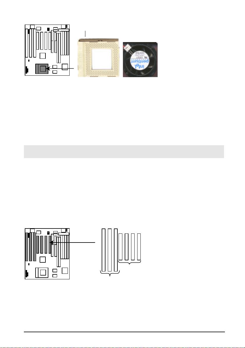
3.2 Installation of the CPU
The SQ574 comes with a 321-pin ZIF socket 7 for installing the CPU. The Socket 7 will also
support future Pentium up-grade processors. It is strongly recommended that a heatsink and
CPU cooling fan be used to prevent the CPU from overheating. (Tip) Applying a thermal
jelly between the CPU and the heatsink/fan will help cool the CPU.
To install a CPU, remember to take the following precautions against static electric
discharge. The basic procedure is as follows:
NOTICE: When installing the CPU into the CPU socket, be sure that PIN 1 of the CPU is
in the same corner as PIN 1 of socket. The CPU is an extremely sensitive electrical
component and can be easily damaged by static electricity.
SQ574 3-5
1) Turn off your system and disconnect the power source.
2) Remove the existing CPU from the ZIF socket by pulling the ZIF lever upwards at a 90
degree angle.
3) Insert the CPU with the correct orientation as shown below. Use the notched (white
dot) corner of the CPU as your guide. The notch in the corner of the CPU should
correspond with PIN 1 of the ZIF socket (Notice: Pin 1 is the blank corner of the ZIF
socket with one hole missing).
4) Once the CPU is inserted close the socket’s lever.
WARNING: Without a fan, the CPU can overheat and will cause damage to both the CPU
and the SQ574 mainboard.
3.3 Installation of Expansion Slots:
3.3.1 ISA & PCI Slots
There are two types of ISA expansion cards, design-Legacy and PnP (Plug & Play). For
Legacy cards you must set the cards’ jumpers manually. For Plug & Play cards, your system
will adjust the IRQs automatically. You can verify the IRQ allocation either by using
Microsoft’s Diagnostic (MSD.EXE) utility which is in the Windows directory or through the
Windows 95 resources menu.
16-bit ISA Slot
32-bit PCI Slot

SQ574
3-6
3.3.2 Installation Procedure:
The SQ574 has 7 expansion slots on-board. Three are 16-bit ISA Bus expansion connectors
and four are 32-bit PCI expansion slots. One of the expansion slots is shared by the
connectors and will accommodate either an ISA or a PCI expansion card, but not both at the
same time. All four PCI expansion slots accept PCI Bus master cards and fully supported by
PCI 2.1 specifications.
To install expansion cards, please read the expansion card’s documentation,which shipped
with the expansion card, for instructions.
NOTICE: Some expansion cards require an IRQ to work and may cause a conflict. There
are total of 16 IRQs but only 6 are free for expansion cards. In case of a conflict please
contact the system manufacturer for technical support.
3.4 Installation of IDE, I/O cables connection
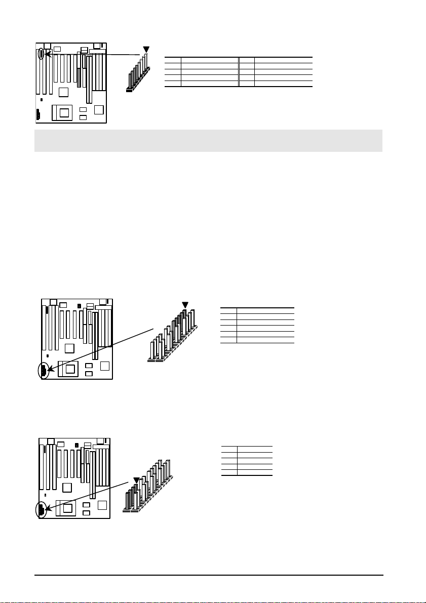
3.4.1 Primary IDE Connector (40-pin block) (J14)
This connector supports two primary channel IDE devices via a ribbon cable. When two
IDE devices are installed using the primary IDE connector make sure that the second IDE
device is set to slave mode as indicated in the device’s manual.
Pin Signal Name Pin Signal Name
1Reset IDE 2Ground
3Host Data 7 4Host Data 8
5Host Data 6 6Host Data 9
7Host Data 5 8Host Data 10
9Host Data 4 10 Host Data 11
11 Host Data 3 12 Host Data 12
13 Host Data 2 14 Host Data 13
15 Host Data 1 16 Host Data 14
17 Host Data 0 18 Host Data 15
19 Ground 20 Key
21 DDRQ0 (DDRQ1) 22 Ground
23 I/O Write # 24 Ground
25 I/O Read # 26 Ground
27 IOCHRD 28 +5V V pull-up
29 DDACK0 (DDACK1) # 30 Ground
31 IRQ14 (IRQ15) 32 Reserved
33 Addr 1 34 Reserved
35 Addr 0 36 Addr 2
37 Chip Select 1P (1S) # 38 Chip Select 3P (3S)
39 Activity# 40 Ground
WARNING: When you connect a ribbon cable to these ports, you must orient the cable
connector so that the PIN 1 edge of the cable is at the PIN 1 end of the on-board connector.
3.4.2 Secondary IDE Connector (40-pin block) (J15)
This connector supports two secondary channel IDE devices and 120MB Floppy drives via a
ribbon cable. When two IDE devices are installed using the secondary IDE connector make
sure that the second IDE device is adjusted to slave mode as instructed in the device’s
manual.

SQ574 3-7
Pin Signal Name Pin Signal Name
1Reset IDE 2Ground
3Host Data 7 4Host Data 8
5Host Data 6 6Host Data 9
7Host Data 5 8Host Data 10
9Host Data 4 10 Host Data 11
11 Host Data 3 12 Host Data 12
13 Host Data 2 14 Host Data 13
15 Host Data 1 16 Host Data 14
17 Host Data 0 18 Host Data 15
19 Ground 20 Key
21 DDRQ0 (DDRQ1) 22 Ground
23 I/OWrite # 24 Ground
25 I/O Read # 26 Ground
27 IOCHRD 28 +5V V pull-up
29 DDACK0 (DDACK1) # 30 Ground
31 IRQ14 (IRQ15) 32 Reserved
33 Addr 1 34 Reserved
35 Addr 0 36 Addr 2
37 Chip Select 1P (1S) # 38 Chip Select 3P (3S)
39 Activity# 40 Ground
WARNING: When you connect a ribbon cable to these ports, you must orient the cable
connector so that the PIN 1 edge of the cable is at the PIN 1 end of the on-board connector.
3.4.3 Floppy Drive Connector (34-pin block) (J9)
The FDC sub-system can control three types (1.2, 1.44, and 2.88MB) of floppy drivers or
compatible tape drives. Connection to floppy drives is via a header (J9). The floppy disk
interface includes 48mA drivers and Schmit inputs on the drive interface.
Pin Signal Name Pin Signal Name
1Ground 2DENSEL
3Ground 4TP
5Key 6FDENIN#
7Ground 8FDINDX#
9Ground 10 FDM00#
11 Ground 12 FDDS1#
13 Ground 14 FDDS0#
15 Ground 16 FDM01#
17 MSEN1 18 FDDIR#
19 Ground 20 FDSTEP#
21 Ground 22 FDWD#
23 Ground 24 FDWE#
25 Ground 26 FDTRK0#
27 MSEN0 28 FDWPD#
29 Ground 30 FDRDATA#
31 Ground 32 FDHEAD#
33 Ground 34 DSKCHG#
WARNING: When you connect a ribbon cable to this port, you must orient the cable
connector so that the PIN 1 edge of the cable is at the PIN 1 end of the on-board port.
3.4.4 Universal Serial Bus (USB) Port
This SQ574 mainboard has two USB on-board header. USB devices provide a more
convenient operating environment and improve data transferring capacity. True Plug-and-
Play, this new bus technology will support over 127 different peripherals through a Hub.
SQ574
3-8
Pin Signal Name (USB1) Pin Signal Name (USB2)
1+5V 5+5V
2USB0- 6USB1-
3USB0+ 7USB1+
4Ground 8Ground
WARNING: When you connect a ribbon cable to these ports, you must orient the cable
connector so that the PIN 1 edge of the cable is at the PIN 1 end of the on-board connector.
3.4.5 Power Input Connector (12-pin block) (J8)
This connector supports a standard AT power supply. When connecting, make sure the lock
key matches the hook attached on a power supply cable. The power cord should be
unplugged when you connect it.
3.4.6 Keylock and Power_On/Suspended LED Connector (5-pin)
(J13)
The SQ574 supports one straight 5 pin header for connecting to front pannel
Power/Suspended LED indicator. The Power LED will become blinking once the system get
into Suspend Mode.
Pin Signal Name
1LED+
2No Connect
3LED-
4Keylock
5Ground
3.4.7 HDD LED Connector (4-pin) (J12)
The SQ574 supports one straight 4 pin header for connecting to front pannel Hard Disk
activity LED indicator.
Pin Signal Name
1LED+
2LED-
3LED-
4LED+

SQ574 3-9
3.4.8 Reset Switch Connector (2-pin) (J16)
This connector supports the front pannel case-mounted reset. It is advised that the reset
switch be used for rebooting the system in order to extend the life of the system’s power
supply.
Pin Signal Name
1Reset
2Ground
3.4.9 Speaker Connector (4-pin) (J17)
A 1x4 straight header is available to drive a chassis-mounted speaker if desired.
Pin Signal Name
1Speaker+
2No connect
3No connect
4Speaker-
3.4.10 IrDA connector (6-pin) (J11)
The SQ574 mainboard offers an IrDA function. The case must reserve space for the IR
module if you want to use the IrDA function. This connector supports optional wireless
transmission and reception of infrared data. The module mounts in a small opening on the
system case that supports this feature. The efficient distance is 100cm and the transfer rate is
1.44M KB/sec.
Pin Signal Name
1+5V
2Key
3IrRX
4Ground
5IrTX
6Reserve
IMPORTANT: You must configure this feature through the BIOS. The IR module is
supported by the mainboard via a 6-pin connector and ribbon cable.
3.4.11 Fan_On Control (J7)
This connector supports the on board fan power output, the Fan can be shut down once the
system get into Suspended Mode.

SQ574
3-10
Pin Signal Name
1Fan_On
2+12V
3Fan_On
3.4.12 PS/2 Keyboard (J2) and Mouse Connector (J3)
The SQ574 mainboard offers 1 PS/2 Keyboard and 1 PS/2 Mouse port as below.
PS/2 Mouse
Keyboard
Pin Signal Name
1DATA
2Key
3Ground
4+5V (Fused)
5Clock
6No connect
3.4.13 Parallel Port Connector (26-pin Block) (J1)
The motherboard includes a bi-directional parallel port (EPP/ECP compatible). The parallel
port is capable of being disabled or remapped to either the secondary LPT address or the
primary LPT address through BIOS if other parallel ports are installed. The parallel port
contains 12mA source output drivers on the drive interface and incorporates Chip Protect
circuitry for protection against damage due to printer’s power being on.
Pin Signal Name Pin Signal Name
1STROBE# 14 AUTOFD#
2DATA BIT 0 15 FAULT#
3DATA BIT 1 16 PINIT#
4DATA BIT 2 17 SLCT IN#
5DATA BIT 3 18 Ground
6DATA BIT 4 19 Ground
7DATA BIT 5 20 Ground
8DATA BIT 6 21 Ground
9DATA BIT 7 22 Ground
10 ACK# 23 Ground
11 BUSY 24 Ground
12 PEERROR 25 Ground
13 SLCTt
Parallel Port
3.4.14 Serial Port (J4/J5)
The SQ574 has two serial ports. The electrical characteristics are compliant with the EIA-
232-D Serial Communications Specifications. The serial ports may be remapped above other
installable serial ports or disabled through the BIOS.

SQ574 3-11
Pin Signal Name
1DCD
2TXD
3RXD
4DTR
5GND
6DSR
7RTS
8CTS
9RI
COM1
COM2
3.4.15 SB-LINK Connector (J15)
To support the legacy Sound Blaster compatible Audio to the PCI bus.
SB-LINK
Pin Signal Name
1PCPCIGNTN
2DGND
3KEY
4PCPCIREQN
5DGND
6SERIRQ

Table of contents
Other BCM Motherboard manuals


