AN1499 Rev.0.00 Page 2 of 4
Oct 2, 2009
ISL28133EVAL1Z
Amplifier Configuration
(Figure 2)
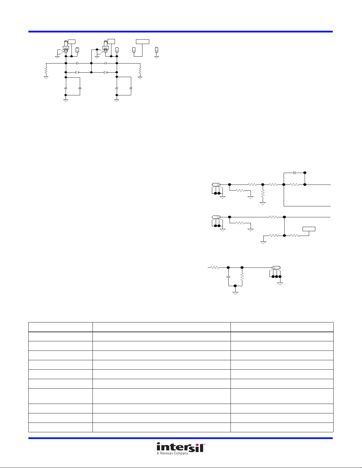
The schematic of the op amp with the components
supplied is shown in Figure 2, with a closed loop gain of
10,000. The circuit implements a Hi-Z differential input
with unbalanced common mode impedance. The
differential amplifier gain is expressed in Equation 1:
where: RF = RGand RIN+ = RIN- and the differential
input impedance is ~1M with VREF at GND. The IN- input
connects to the amplifier summing junction and it’s
impedance to ground is a low 100
The impedance of the
IN+ input to ground is much higher at 1.001M
to VREF.
For single-ended input inverting operation (G = -10001),
the IN+ input is grounded and the signal is supplied to
the IN- input. VREF must be connected to a reference
voltage between the V+ and V- supply rails. For
non-inverting operation (G = 10,000), the IN- input is
grounded and the signal is supplied to the IN+ input. The
non-inverting gain is strongly dependent on any
resistance from IN- to GND. For good gain accuracy, a 0
resistor should be installed on the empty R7 pads.
User-selectable Options
(Figures 3 and 4)
Component pads are included to enable a variety of
user-selectable circuits to be added to the amplifier
inputs, the VREF input, outputs and the amplifier
feedback loops.
A voltage divider and filter option (Figure 3) can be
added to establish a power supply-tracking common
mode reference at the VREF input. The inverting and
non-inverting inputs have additional resistor placements
for adding input attenuation, or to establish input DC
offsets through the VREF pin.
The output (Figure 4) also has additional resistor and
capacitor placements for filtering and loading.
NOTE: Operational amplifiers are sensitive to output
capacitance and may oscillate. In the event of oscillation,
reduce output capacitance by using shorter cables, or
add a resistor in series with the output.
R4
D2D1
R16
C2 C4
J8
J11
J9 J10
J7 J13
DNP
DNP
S1AB
1µF 1µF
S1AB
VREF
V+
V-
0.1µF
C7
C1
0.01µF
0.1µF
C8
C5
0.01µF
FIGURE 2. POWER SUPPLY CIRCUIT
VOUT VIN+
VIN-RF
RIN–VREF
+= (EQ. 1)
IN +
IN -
DNP
R7
R5
J2
J1 R1
R2
R12
R15
R13
R11R9
10k
DNP
DNP
0
10k
DNP
100k
OPEN
100k
VREF
TO IN -
TO IN +
FROM OUT
FIGURE 3. INPUT STAGE
OUTPUT
R18
J12
C6
R17
DNP
OPEN
0
FIGURE 4. OUTPUT STAGE
TABLE 1. ISL28133EVAL1Z COMPONENTS PARTS LIST
DEVICE # DESCRIPTION COMMENTS
C2, C4 CAP, SMD, 0603, 1µF, 25V, 10%, X7R, ROHS Power Supply Decoupling
C1, C5 CAP, SMD, 0603, 0.1µF, 25V, 10%, X7R, ROHS Power Supply Decoupling
C7, C8 CAP, SMD, 0603, 0.01µF, 25V, 10%, X7R , ROHS Power Supply Decoupling
C3, C6 CAP, SMD, 0603, DNP-PLACE HOLDER, ROHS User selectable capacitors - not populated
D1, D2 DIODE-RECTIFIER, SMD, SOD-123, 2P, 40V, 0.5A, ROHS Reverse Power Protection
U1 (ISL28133EVAL1Z) ISL28133FHZ-T7, IC-RAIL-TO-RAIL OP AMP, SOT-23, ROHS
R1-R4, R6-R8, R10, R13,
R14, R16, R17, R19, R21 RESISTOR, SMD, 0603, 0.1%, MF, DNP-PLACE HOLDER User selectable resistors - not populated
R5, R18 RES, SMD, 0603, 0, 1/10W, TF, ROHS 0user selectable resistors
R9, R12 RES, SMD, 0603, 100, 1/10W, 1%, TF, ROHS Gain resistors
R11, R15 RES, SMD, 0603, 1M, 1/10W, 1%, TF, ROHS Gain resistors


