IDT P9242-G-EVK User manual

P9242-G-EVK Evaluation Board User Manual
© 2019 Integrated Device Technology, Inc.
1
February 17, 2019
Description
The P9242-G-EVK Evaluation Board demonstrates the features of
the P9242-G 15W Wireless Power Transmitter (TX) with a fixed
frequency. It is intended to evaluate the functionality and
performance of the P9242-G when combined with a Qi power
receiver in a wireless charging system. The P9242-G-EVK offers
the flexibility to select parameters, such as Q-factor threshold, LED
pattern, power loss FOD threshold, and external temperature
sensing function. The printed circuit board (PCB) has four layers. It
can be used with the user’s WPC-1.2.4 compliant receiver.
The high-efficiency, turnkey reference design is supported by
comprehensive online, digital resources to significantly expedite
the design-in effort and enable rapid prototyping.
Kit Contents
P9242-G-EVK Evaluation Board
Adaptor: 18V/1.38A
Features
P9242-G Evaluation Board with support for WPC-1.2.4
Up to 15W output power
Adjustable open Q-factor threshold
Adjustable power loss FOD threshold
Adjustable temperature shutdown
Two programmable LED status indicators
Four-layer PCB
Fully assembled with test points and coil fixture
P9242-G-EVK Mass-Market Evaluation Board
12V/1.38A AC Adapter (Not to scale)
P9242-G-EVKEvaluationBoardUserManual
©2018IntegratedDeviceTechnology,Inc.
13
February 17, 2019
Important Notes
Disclaimer
Integrated Device Technology, Inc. and its affiliated companies (herein referred to as “IDT”) shall not be liable for any damages arising out of defects resulting from
(i) delivered hardware or software
(ii) non-observance of instructions contained in this manual and in any other documentation provided to user, or
(iii) misuse, abuse, use under abnormal conditions, or alteration by anyone other than IDT.
TO THE EXTENT PERMITTED BY LAW, IDT HEREBY EXPRESSLY DISCLAIMS AND USER EXPRESSLY WAIVES ANY AND ALL WARRANTIES, WHETHER
EXPRESS, IMPLIED, OR STATUTORY, INCLUDING, WITHOUT LIMITATION, IMPLIED WARRANTIES OF MERCHANTABILITY AND OF FITNESS FOR A
PARTICULAR PURPOSE, STATUTORY WARRANTY OF NON-INFRINGEMENT, AND ANY OTHER WARRANTY THAT MAY ARISE BY REASON OF USAGE
OF TRADE, CUSTOM, OR COURSE OF DEALING.
Restrictions in Use
IDT’s [Kit Name], consisting of the [Kit Contents and Software], is designed for [list of intended purposes] only. IDT’s [Kit Name and Software] must not be used
for [list of prohibited uses].
Contents
1. Hardware Setup..........................................................................................................................................................................................15
Required or Recommended User Equipment....................................................................................................................................15
2. Usage Guide...............................................................................................................................................................................................15
Overview of the P9242-G-EVK..........................................................................................................................................................15
LED Pattern Selection .......................................................................................................................................................................16
External Temperature Sensing (TS)..................................................................................................................................................18
External Buck Regulator....................................................................................................................................................................19
Bypass Path of the External Buck Regulator.....................................................................................................................................20
External Oscillator .............................................................................................................................................................................21
Resonant Capacitor...........................................................................................................................................................................22
Q-factor Detection and Open Advanced Q-factor..............................................................................................................................23
Selection of Input Source and Operation Mode.................................................................................................................................25
Transmitter Coil .................................................................................................................................................................................26
3. P9242-G Evaluation Board Schematic .......................................................................................................................................................27
4. Bill of Materials (BOM)................................................................................................................................................................................28
5. Board Layout ..............................................................................................................................................................................................32
6. Ordering Information...................................................................................................................................................................................35
7. Revision History..........................................................................................................................................................................................35

P9242-G-EVKEvaluationBoardUserManual
©2018IntegratedDeviceTechnology,Inc.
14
February 17, 2019
List of Figures
Figure 1. P9242-G V3.8 Evaluation Board Features ........................................................................................................................................15
Figure 2. P9242-G V3.8 Evaluation Board Detail .............................................................................................................................................16
Figure 3. R61 and R62 Schematic Location .....................................................................................................................................................17
Figure 4. R61 and R62 PCB Location...............................................................................................................................................................18
Figure 5. TH_COIL1, R60, and RC67 Schematic Location ..............................................................................................................................18
Figure 6. TH_COIL1, R60, and RC67 PCB Location........................................................................................................................................19
Figure 7. Buck Regulator Schematic Location..................................................................................................................................................19
Figure 8. Buck Regulator PCB Location ...........................................................................................................................................................20
Figure 9. Bypass Path Schematic Location ......................................................................................................................................................20
Figure 10. Buck Regulator PCB Location ...........................................................................................................................................................21
Figure 11. Bypass Path Schematic Location ......................................................................................................................................................21
Figure 12. Buck Regulator PCB Location ...........................................................................................................................................................22
Figure 13. Q-factor Detection Schematic Location .............................................................................................................................................23
Figure 14. Q-factor PCB Location.......................................................................................................................................................................24
Figure 15. Input Source Selection Jumpers on the PCB ....................................................................................................................................25
Figure 16. Silkscreen –Top of Board .................................................................................................................................................................32
Figure 17. Copper –Top Layer...........................................................................................................................................................................33
Figure 18. Copper L1 Layer................................................................................................................................................................................33
Figure 19. Copper L2 Layer................................................................................................................................................................................34
Figure 20. Copper Bottom ..................................................................................................................................................................................34
List of Tables
Table 1. LED Pattern Selection .......................................................................................................................................................................17
Table 2. External Oscillator Selection..............................................................................................................................................................21
Table 3. Voltage on GPIO_A2 vs. Advanced Q-factor Threshold....................................................................................................................24
Table 4. P9242-G-EVK Operation Modes .......................................................................................................................................................26
Table 5. Recommend Coil Manufacturer.........................................................................................................................................................26
P9242-G-EVKEvaluationBoardUserManual
©2018IntegratedDeviceTechnology,Inc.
15
February 17, 2019
1. Hardware Setup
Required or Recommended User Equipment
The following additional lab equipment is required for using the kit:
P9221-G-EVK Transmitter Evaluation Board or any WPC-1.2.4 compliant receiver
Power supply capable of 18V/1.38A
2. Usage Guide
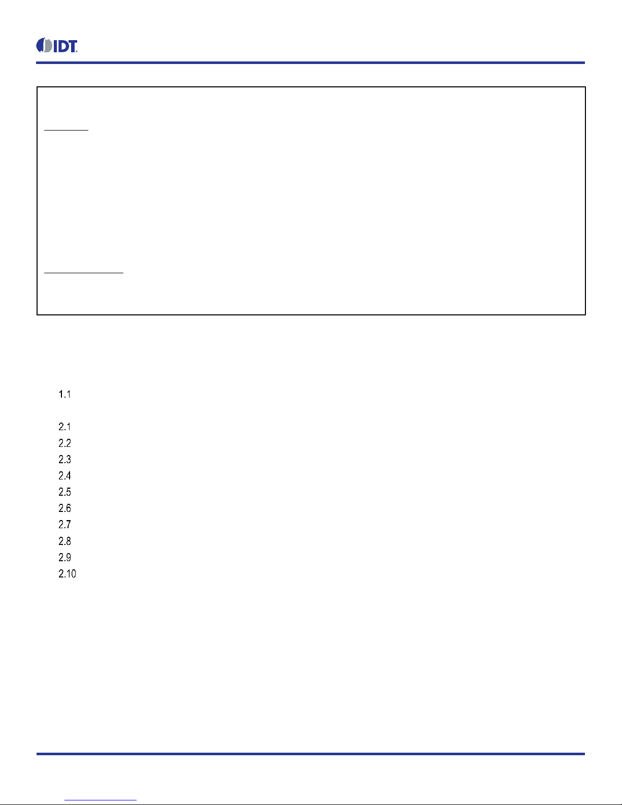
Overview of the P9242-G-EVK
Figure 1. P9242-G V3.8 Evaluation Board Features
Tx Coil
Input Select Jumpers
Vin Power Connector: Micro-USB
Vin Connector: USB-C
Vin PowerConnector:Barrel
Green LED and Red LED
J4 I2CConnector
J5 IDT-Reserved Connector –Do Not Use
P9242-G-EVKEvaluationBoardUserManual
©2018IntegratedDeviceTechnology,Inc.
16
February 17, 2019
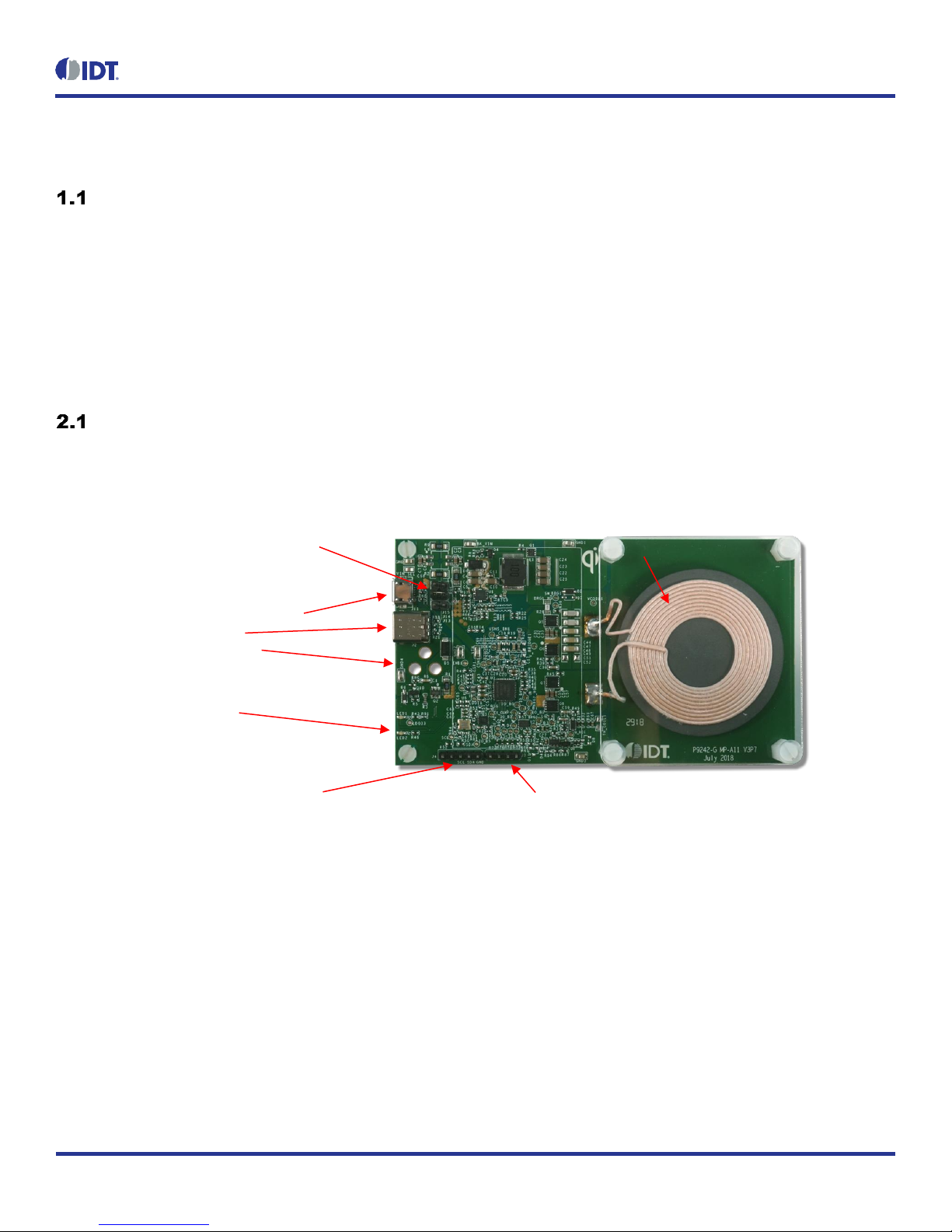
Figure 2. P9242-G V3.8 Evaluation Board Detail
Note: The P9242-GB was used instead of the P9242-G IC on the P9242-G V3.8 Evaluation Board. The P9242-G has firmware pre-programmed
into one-time programmable memory and does not let users customize the firmware. The P9242-GB also offers a pre-programmed bootloader
that must be used in conjunction with an external flash. Firmware is loaded into the external flash. Users can customize the firmware in external
flash. There is no functionality difference of the P9242-G V3.8 Evaluation Board using the P9242-G IC or the P9242-GB with external flash.
LED Pattern Selection
The P9242-G-EVK uses two LEDs (LED1 and LED2; see Figure 1) to indicate the power transfer status, faults, and operating modes. The LEDs
are connected to the LED1 and LED2 pins as shown in the P9242-G-EVK schematics.
Buck Compensation
Circuit
External
Oscillator Circuit
P9242-GB IC
Flash IC
Buck IC
Buck Power
Stage Filter
Resonant
Capacitors
High Voltage Input OVP
Circuit
Q-factor
Detection
Circuit
External Flash for
development

P9242-G-EVKEvaluationBoardUserManual
©2018IntegratedDeviceTechnology,Inc.
17
February 17, 2019
Table 1. LED Pattern Selection
Option
Voltage on GPIO_A3 Pin
LED1/LED2 Pin
Status
Standby
Transfer
Complete
Fault
1
0V ≤ VGPIO_A3 < 0.1V;
0.7V < VGPIO_A3 < 0.8V;
1.4V < VGPIO_A3 < 1.5V;
2.1V < VGPIO_A3 < 2.4V
LED2
Off
On
Off
Off
LED1
Off
Off
Off
Blink 4Hz
2
0.1V < VGPIO_A3 < 0.2V;
0.8V < VGPIO_A3 < 0.9V;
1.5 V< VGPIO_A3 < 1.6V
LED2
On
On
Off
Off
LED1
On
Off
Off
Blink 4Hz
3
0.2V < VGPIO_A3 < 0.3V;
0.9V < VGPIO_A3 < 1.0V;
1.6V < VGPIO_A3 < 1.7V
LED2
Off
Blink 1Hz
On
Blink 4Hz
LED1
Off
Off
Off
Off
4
0.3V < VGPIO_A3 < 0.4V;
1.0V < VGPIO_A3 < 1.1V;
1.7V < VGPIO_A3 < 1.8V
LED2
Off
On
Off
Blink 4Hz
LED1
Off
Off
Off
Off
5
0.4V < VGPIO_A3 < 0.5V;
1.1V < VGPIO_A3 < 1.2V;
1.8V < VGPIO_A3 < 1.9V
LED2
On
Blink 1Hz
On
Off
LED1
On
Off
Off
Blink 4Hz
6
0.5V < VGPIO_A3 < 0.6V;
1.2V < VGPIO_A3 < 1.3V;
1.9V < VGPIO_A3 < 2.0V
LED2
Off
Off
On
Off
LED1
Off
On
Off
Blink 4Hz
7
0.6V < VGPIO_A3 < 0.7V;
1.3V < VGPIO_A3 < 1.4V;
2.0V < VGPIO_A3 < 2.1V
LED2
Off
Blink 1Hz
On
Off
LED1
Off
Off
Off
Blink 4Hz
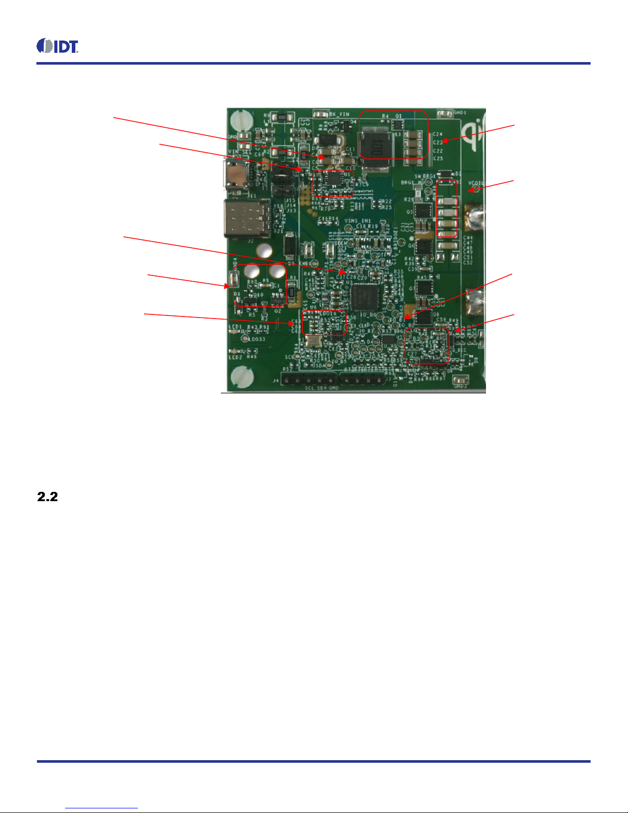
The LED patterns can be selected by setting the voltage on the GPIO_A3 pin through the resistor divider R61 and R62 (for options, see Table 1).
On the evaluation board, the GPIO_A3 pin is pulled up to GND through R62. R61 is unpopulated; therefore, option 1 is the default option.
Figure 3. R61 and R62 Schematic Location
FOD AND LED PAT
R58 20K R59 10k
R61 10K
FOD_ADJ
R62
10k
LDO33
LED_PAT
P9242-G-EVKEvaluationBoardUserManual
©2018IntegratedDeviceTechnology,Inc.
18
February 17, 2019
Figure 4. R61 and R62 PCB Location
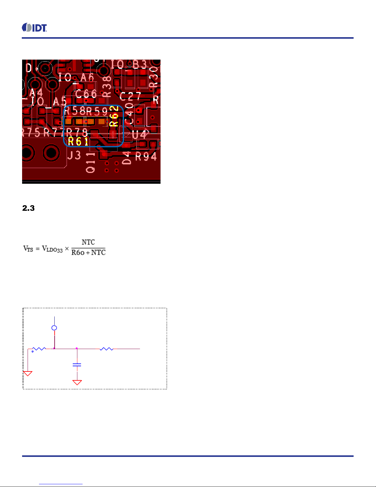
External Temperature Sensing (TS)
The P9242-G includes an optional temperature sense input pin, TS, that is used to monitor a remote temperature, such as for a coil or a battery
charger. The TS pin voltage can be calculated using Equation 1.
Equation 1
Where NTC is the thermistor’s resistance (RTH1) and R60 is the pull-up resistor connected to the 3.3V supply voltage on the P9242-G Evaluation
Board. The over–temperature shutdown is triggered if the voltage on the TS pin is lower than 0.6V, and recovers at 0.8V. The RTH1 is not
populated on the P9242-G Evaluation Board.
Figure 5. TH_COIL1, R60, and RC67 Schematic Location
R60 10K
C67
0.1uF
OTP
OTP
t
TH_Coil1
COIL TEMPERATURE SENSING
LDO33
P9242-G-EVKEvaluationBoardUserManual
©2018IntegratedDeviceTechnology,Inc.
19
February 17, 2019
Figure 6. TH_COIL1, R60, and RC67 PCB Location
External Buck Regulator
To operate at a fixed 127.7kHz frequency, the P9242-G-EVK has adopted an MP2229 Buck IC to adjust the power transfer between the transmitter
and receiver. GPIO_A4 and GPIO_B4 are assigned to adjust the MP2229 FB control. The MP2229 is operating at a fixed 500kHz frequency on
the board. The Buck regulator power stage is designed to accommodate a wide range of input voltages. The feedback loop combined with the
external PWM signal are designed for the MP2229, and are not recommended to be changed. The resolution of the MP2229 is about 35mV. The
Buck and external components in the PCB layout should be isolated from any noise generating circuits.
Figure 7. Buck Regulator Schematic Location
R13 18K
C10
22uF
R79
NP
R16
5.1K
BK_EN
C6
22uF
C11
0.1uF
BK_VIN
C14
NPC15
0.1uF
Q12
NP
C71 NP
C9 0.1uF
R96
0
R7 10
R11
150K
C4
22uF
R97
0
C12
0.1uF
C5
0.1uF
L3 10uH
BK_ADJ
R14 3.3K
BK_VIN
U1
MP2229
VCC
9
EN
4
LPM
5
FREQ/SYNC
8
BST 10
SW1 2
FB 6
SS 7
IN 3
SW2 11
GND1
1
INPAD 15
R67
0
C16
0.1uF
C13
NP
R12
30k
BK_FB
R95
10K
R66
NP
R15
30k
D6
SMAJ20CA-13-F
BK_SW
P9242-G-EVKEvaluationBoardUserManual
©2018IntegratedDeviceTechnology,Inc.
20
February 17, 2019
Figure 8. Buck Regulator PCB Location
Bypass Path of the External Buck Regulator
When the adaptor voltage is 5V only (such as USB DCP or legacy USB 5V adaptors), the P9242-G-EVK supports such adaptors by turning off
the Buck regulator, and then enable a bypass path. The P9242-G will be operating in a variable frequency mode, to adjust the total power
transferred. GPIO_A4 is used to turn on the bypass path.
Figure 9. Bypass Path Schematic Location
Q1
SIA453EDJ-T1_GE3
1
2
3
4
75
6
8
R88 0
BYPASS BUCK OPTIONAL:
NEEDED FOR 5V SUPPORT
R8
100k
R4
100k
BYP_EN
Q4
2N7002
P9242-G-EVKEvaluationBoardUserManual
©2018IntegratedDeviceTechnology,Inc.
21
February 17, 2019
Figure 10. Buck Regulator PCB Location
External Oscillator
To guarantee that the switching frequency is fixed at an accurate 127.7kHz ±6Hz, an external clock IC and a crystal is used to guarantee that the
frequency will be in the range displayed in Table 2. The frequency of the clock IC or MEMS oscillator must be precisely 6.16791MHz to work with
the P9242-G. GPIO_B6 is used to synchronize with the external clock, and GPIO_B5 is recommended to be connected to GND when the external
oscillator is used. Table 2 contains a list of the recommended devices for clock/MEMS.
Table 2. External Oscillator Selection
Type
Vendor
Part Number
Typical Frequency (MHz)
Crystal + Clock IC
IDT
6P40369
6.16791
TXC
7M25000083
25
MEMS Oscillator
ASTMLP-101-6.167910MHZ-T3
6.16791
MEMS Oscillator
DSC6111MI2A-006.1679
6.16791
Figure 11. Bypass Path Schematic Location
C61 NP C62
0.1uFR85
NP
R84
NP
LDO33
R54 10K
R53
10K
R71
NP
C60 NP
R72
NP
R51
NP
R55
33
LDO18
Y1
25MHz
13
24
GREEN
U5
6P40369
DFC0
1
SEL/DFC1
2
VSS
3
XOUT
4
XIN
5
VDD
6
VSS1 12
NC2 11
VDDO 10
NC1 9
NC 8
CLKOUT 7

P9242-G-EVKEvaluationBoardUserManual
©2018IntegratedDeviceTechnology,Inc.
22
February 17, 2019
Figure 12. Buck Regulator PCB Location
Resonant Capacitor
The P9242-G-EVK uses multi-layer ceramic capacitors as the resonant caps. A combination of 100nF/250V/X7R/1206 capacitors and
100nF/100V//C0G/1206 capacitors are used. If class II ceramic capacitors are used as the resonant capacitors, they need to be carefully selected.
The important considerations include the following:
High voltage rating
Stable DC characteristic
Stable AC characteristic
Stable temperature characteristic
P9242-G-EVKEvaluationBoardUserManual
©2018IntegratedDeviceTechnology,Inc.
23
February 17, 2019
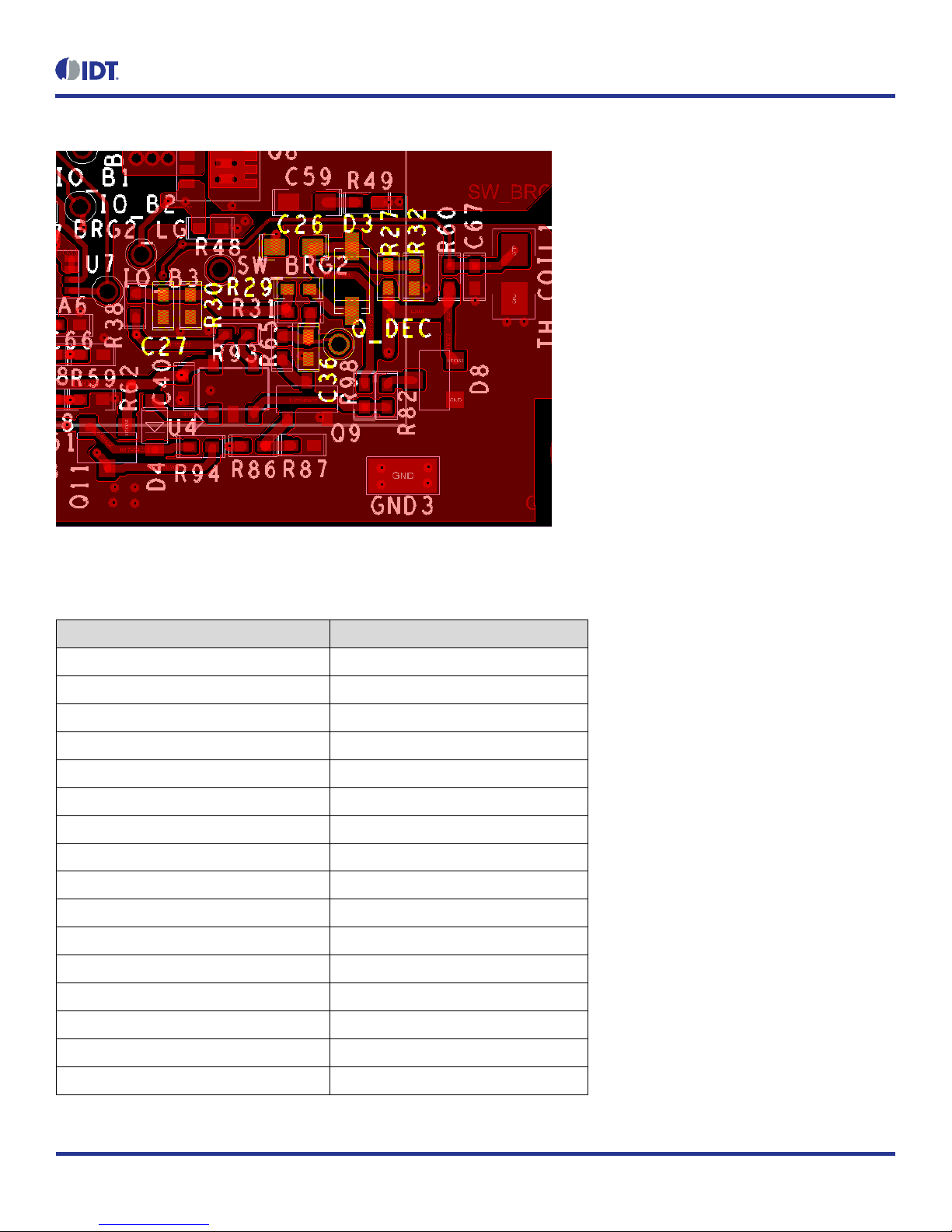
Q-factor Detection and Open Advanced Q-factor
The P9242-G-EVK has implemented the Q-factor detection for WPC EPP receivers. The Q_DEC pin is used to sample the voltage on the coil.
Figure 13 shows the Q-factor detection circuits.
Figure 13. Q-factor Detection Schematic Location
R32
10K
OVP_CTL
C26
1nF
U4MCP6021
4
2
13
5
R94
NP
R29 510
LDO33
R98
100
LDO33
Q_DEC
LDO33
OPTIONAL
Q11
2N3904/TO
R87 100k
R65
10K
D3
BAV21W
R86
0
R30
47K
D8
BAT54S/SOT
C40
0.1uF
R38
NP
R82
0
Q9
2N7002
C36
47pF
R27 51K
C27
2.2nF
R93
0
R31
5.1K
D4
1N4148
P9242-G-EVKEvaluationBoardUserManual
©2018IntegratedDeviceTechnology,Inc.
24
February 17, 2019
Figure 14. Q-factor PCB Location
Table 3 shows how to set up the Advanced Q-factor threshold.
Table 3. Voltage on GPIO_A2 vs. Advanced Q-factor Threshold
Voltage on GPIO_A2
Advanced Open Q-Factor Threshold
0V ≤ VGPIO_A2 < 0.4V
Feature Disabled
0.4V < VGPIO_A2 < 0.5V
13
0.5V < VGPIO_A2 < 0.6V
16
0.6V < VGPIO_A2 < 0.7V
19
0.7V < VGPIO_A2 < 0.8V
22
0.8V < VGPIO_A2 < 0.9V
25
0.9V < VGPIO_A2 < 1V
28
1V < VGPIO_A2 < 1.1V
31
1.1V < VGPIO_A2 < 1.2V
34
1.2V < VGPIO_A2 < 1.3V
37
1.3V < VGPIO_A2 < 1.4V
40
1.4V < VGPIO_A2 < 1.5V
43
1.5V < VGPIO_A2 < 1.6V
46
1.6V < VGPIO_A2 < 1.7V
49
1.7V < VGPIO_A2 < 1.8V
52
1.8V < VGPIO_A2 < 1.9V
55
P9242-G-EVKEvaluationBoardUserManual
©2018IntegratedDeviceTechnology,Inc.
25
February 17, 2019
Voltage on GPIO_A2
Advanced Open Q-Factor Threshold
1.9V < VGPIO_A2 < 2V
58
2V < VGPIO_A2 < 2.1V
61
2.1V < VGPIO_A2 < 2.2V
64
2.2V < VGPIO_A2 < 2.3
67
2.3V < VGPIO_A2 < 2.4V
70
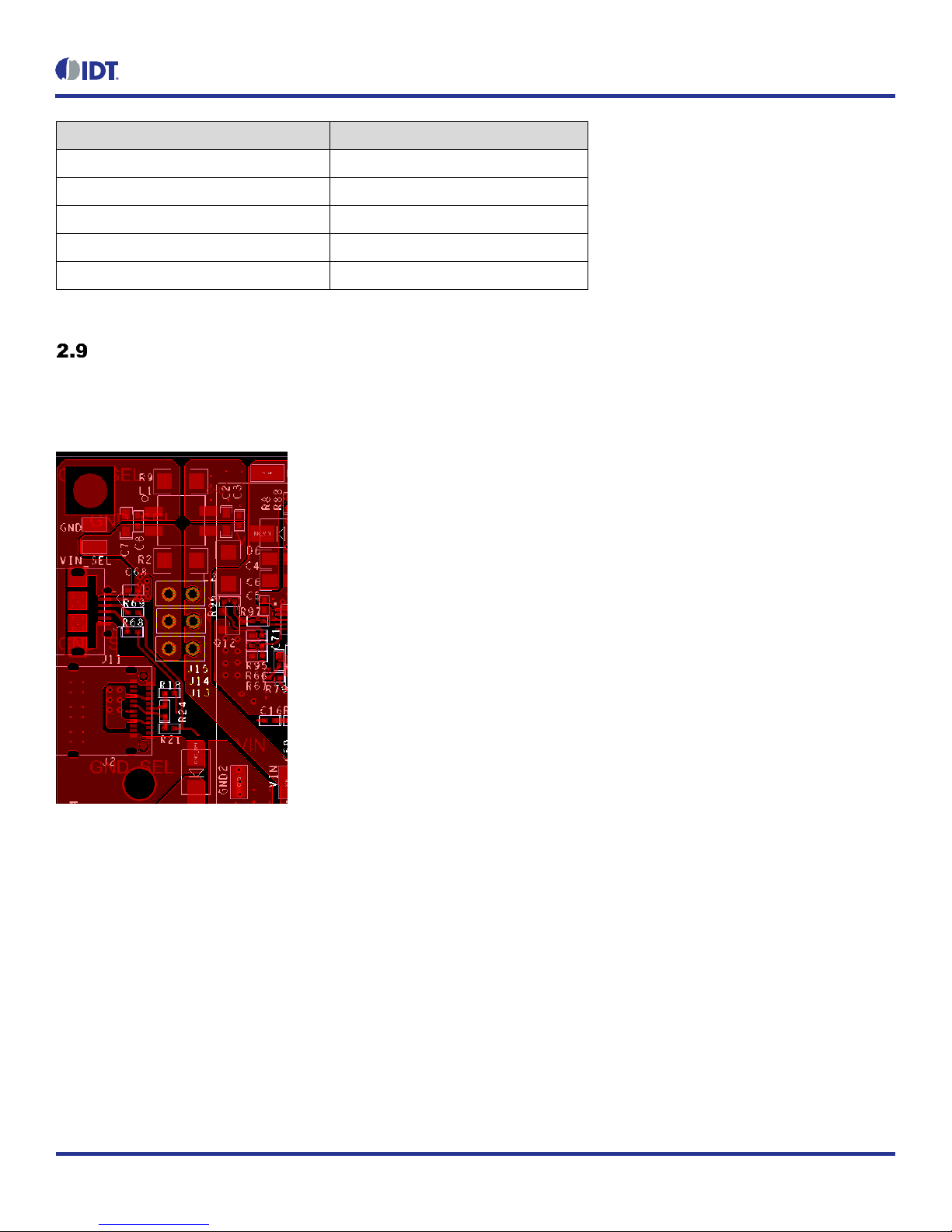
Selection of Input Source and Operation Mode
The P9242-G-EVK supports different types of AD/DC adaptors and connectors. By selecting the jumpers in Figure 15, you can select the USB-
Micro connector, USB-C connector, or DC jack adaptor.
Figure 15. Input Source Selection Jumpers on the PCB

P9242-G-EVKEvaluationBoardUserManual
©2018IntegratedDeviceTechnology,Inc.
26
February 17, 2019
The P9242-G-EVK supports a wide range of input DC sources from 5V to 19V. Based on the input source, the P9242-G-EVK supports different
types of receivers. Table 4 lists the P9242-G-EVK operation modes.
Table 4. P9242-G-EVK Operation Modes
Input Voltage
Rx
Operating Frequency
5V
BPP (Bypass Buck)
110k –148k
9V
BPP 5W
120kHz –127.7kHz
EPP 8W
120kHz –127.7kHz
iPhone 7.5W
127.7kHz
12V
BPP 5W
120kHz –127.7kHz
EPP 10W
120kHz –127.7kHz
Samsung AFC
120kHz - 127.7kHz
iPhone 7.5W
127.7kHz
16-19V
BPP 5W
120kHz –127.7kHz
EPP 15W
120kHz –127.7kHz
Samsung AFC
120kHz –127.7kHz
iPhone 7.5W
127.7kHz
Transmitter Coil
The MP-A11 coils in Table 5 are recommended to be used with the P9242-G transmitter for 15W applications for optimum performance. The
recommended vendor has been tested and verified.
Table 5. Recommend Coil Manufacturer
Output Power
Vendor
Part Number
Inductance at 100kHz
Typical DCR at 25ºC
15W
SUNLORD
MQQTC505030S6R3
6.3uH
38mΩ
15W
CYNTEC
WTCL05054F-6R3ABKS-70
6.3uH
38mΩ
P9242-G-EVKEvaluationBoardUserManual
©2018IntegratedDeviceTechnology,Inc.
27
February 17, 2019
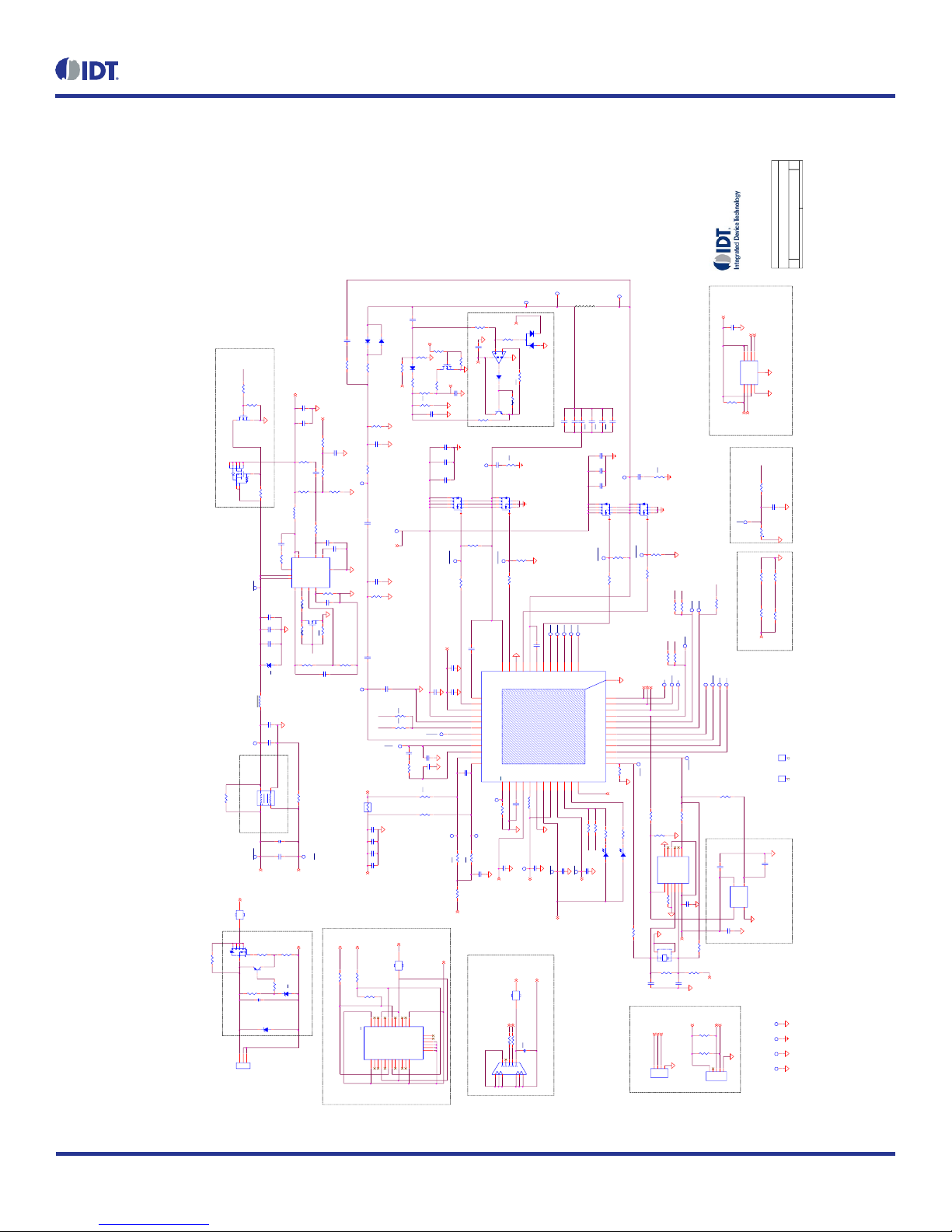
3. P9242-G Evaluation Board Schematic
SW_BRG1
Q1
SIA453EDJ-T1_GE3
1
2
3
4
75
6
8
R13 18K
ENB1
VIN_SEL
D-
GND_SEL
SCL
IO_B1
CURRENT LIMIT/FOD
R32
10K
R2 0
R1 0
OVP_CTL
IDEM
C61 NP
VSNS_IN1
C62
0.1uF
C51 100nF
R60 10K
LDO33
C69 22nF
C43 1uF
C70
NP
OTP
C50
1uF
EX_CLK
C48 100nF
R19
10K
R88 0
OPTIONAL:
when VIN>13V
VDEM1
R70
NP
FOD_ADJ
BYPASS BUCK OPTIONAL:
NEEDED FOR 5V SUPPORT
C26
1nF
R36
100K
C34
0.1uF
J15
1 2
C67
0.1uF
D+
LDO18
R77 0
PROGRAMMING CONNECTOR
GND_SEL
R26
0.02
C10
22uF
OTP
D+
BYP_EN
BK_ADJ
LED2
D2
BAV21W
R85
NP
R8
100k
VCC_5V
VIN_SEL
R4
100k
LED1
2 1
LDO33
R39
0
R79
NP
R16
5.1K
THIS DOCUMENT CONTAINS INFORMATION PROPRIETARY
TO Integrated Device Technology, Inc. (IDT).
USE OR DISCLOSURE WITHOUT THE
WRITTEN PERMISSION OF AN OFFICER OF
IDT IS EXPRESSLY FORBIDDEN
BK_EN
Q6
DMG7430LFG
5
4
16
7
8
2
3
C28
56pF
C65
NP
R6
91K
U4MCP6021
4
2
13
5
R78 NP
R84
NP
C3
0.1uF
C59
22nF
BRG1_HG
R18 0
C6
22uF
CSP1
C11
0.1uF
C52 NP
GPIO_B1
R56
NP
R94
NP
D-
R29 510
LDO33
LDO33
R98
100
DEBUG ONLY
VIN_SEL
C32
10uF
LDO33
U7
W25X40CLUXIG
CS#
1
DO
2
WP#
3
GND
4DI 5
CLK 6
HLD# 7
VCC 8
EPAD
9
Q_DEC
J2USB Type C
GND
A1
TX1+
A2
TX1-
A3
VBUS
A4
CC1
A5
D+
A6
D-
A7
SBU1
A8
VBUS1
A9
RX2-
A10
RX2+
A11
GND1
A12 GND2 B1
TX2+ B2
TX2- B3
VBUS2 B4
CC2 B5
D+1 B6
D-1 B7
SBU2 B8
VBUS3 B9
RX1- B10
RX1+ B11
GND3 B12
GND4
M1
GND5
M2
GND6
M3
GND7
M4
NC
H1
NC1
H2
SDA
R48
100K
VIN_SEL
GND_SEL
OTP
LDO33
T1
TP
1
BK_VIN
R37
NP
D1
DDZ22ASF-7DICT
Q2
Si3417
C30
0.1uF
IO_B5
OVP_CTL
C39
22nF
GND4
R58 20K
C25
22uF
IO_B2
R23
200K
OPTIONAL
J13
1 2
C14
NP
L2 0
1206
R9 0
C15
0.1uF
R59 10k
SW_BRG2
R42
100K
Q11
2N3904/TO
VIN1
R87 100k
C46 0.1uF
Q12
NP
R65
10K
GND_SEL
GPIO_B2
D3
BAV21W
LX2
R54 10K
J14
1 2
NP
C71 NP
GND1
C53
1uF
R22
10
MP-A11
LDO33
R35 22
C9 0.1uF
R53
10K
C37
1uF
R69 0
VIN
SW_BRG1
R96
0
R52
5.1k
R33
NP
R7 10
LDO33
C63
NP
C42
10uF
Q5
DMG7430LFG
5
4
16
7
8
2
3
R86
0
R11
150K
R73 0
D7 NP
GPIO_B1
R57
100K
R30
47K
SCL
R89
NP
Q7
DMG7430LFG
5
4
16
7
8
2
3
C66
0.1uF
C4
22uF
OTP
VCC_5V SW_BRG2
R5 10k
C57
0.1uF
V_BRIDGE1
C17
NP
C35
10uF
2x100NF/COG/1206/100V+
3x100NF/X7R/1206/250V
C29
680pF
EX_CLK
ISNS_OUT
OPTIONAL
IO_A2
VBRIDGE
R97
0
USB-MICRO CONNECTOR, OPTIONAL
OPTIONAL:
FOR DEVELOPMENT ONLY
C12
0.1uF
R47 22
D+
C5
0.1uF
VCOIL1
GND
D-
GPIO_B0
R68 0
LED_PAT
D8
BAT54S/SOT
BRG2_HG
C18 22nF
L3 10uH
USB-C CONNECTOR, OPTIONAL
C40
0.1uF
Q_DEC
SDA
BK_ADJ
R14 3.3K
R75 NP
IO_A3
IO_B3
R38
NP
NP
SDA
C21
22nF
R61 10K
FOD_ADJ
U6
DSC6111MI2A-006. 1679
OOE/ST
1
GND
2OUT 3
VDD 4
BK_VIN
R71
NP
SDA
U1
MP2229
VCC
9
EN
4
LPM
5
FREQ/SYNC
8
BST 10
SW1 2
FB 6
SS 7
IN 3
SW2 11
GND1
1
INPAD 15
BYP_EN
D+
GPIO_B3
C2
10uF
C1
0.1uF
VCC_5V
GPIO_B0
C68
0.1uF
C19
5.6nF
R91 NP
C8
0.1uF
RED
t
TH_Coil1
VIN
GND3
J1
R25
10
IO_B0
IO_A6
C47 100nF
BK_VO
C60 NP
R67
0
R43 1K
Q8
DMG7430LFG
5
4
16
7
8
2
3
BK_VO
R72
NP
VIN_SEL
SLD
SLD
VCC
D-
D+
ID
GND
J11
usb_micro_ab
1
2
3
4
56
7
8
9
10
11
LED2
2 1
C44 100nF
T2
TP
1
GPIO_B3
OPTIONAL:
6.16791MHZ +/-20PPM
NEED FW UPDATE
COIL TEMPERATURE SENSING
C16
0.1uF
BRG2_LG
R24
NP
C33
0.1uF
R92 NP
SW_BRG2
R44 22
C13
NP
Title
Size Document Number Rev
Date: Sheet of
3.8
P9242-G MP-A11 DEMO SCHEMATIC V3P8
Custom
1 1Saturday , July 07, 2018
R51
NP
LDO33
C56
10uF
Q_DEC
IO_A5
R55
33
LDO33
D+
R49
0
LDO18
R76 0
D+
R12
30k
OVP_CTL
D-
C23
22uF
FOD_ADJ
LED_PAT
L1
ACM4520
1
2 3
4
BK_ADJ
R82
0
C20
680p
D-
BRG1_LG
ISNS_IN
BK_FB
LDO33
R20
2.4K
VBRIDGE
IO_A4
R62
10k
R50
5.1k
C7
10uF
VCC5V1
C55
10uF
Q9
2N7002
IO_B4
BYP_EN
C36
47pF
R17
NP
C64
0.1uF
P9242-G
U3
EN
1
GND
2
PREG
3
VIN
4
SW_S
5
GND1
6
LDO33
7
VIN_LDO
8
LDO18
9
LED1
10
LED2
11
VDDIO
12 GPIO_B0 25
GPIO_B1 26
GPIO_B2 27
GPIO_B3 28
GPIO_B4 29
GH_BRG2 30
BST_BRG2 31
SW_BRG2 32
GL_BRG2 33
GND2 34
GL_BRG1 35
SW_BRG1 36
EP
49
BST_ BRG1 37
GH_BRG1 38
DRV_VIN 39
VBRG_IN 40
GND3 41
TS 42
QDEC 43
VDEM1 44
IDEMI 45
ISNS_OUT 46
CSN 47
CSP 48
GPIO_B5
13
GPIO_B6
14
GPIO_A0
15
GPIO_A1
16
GPIO_A2
17
GPIO_A3
18
GPIO_A4
19
GPIO_A5
20
GPIO_A6
21
GPIO_A7
22
GPIO_B7
23
GPIO_B8
24
C38
0.1uF
C31
10uF
LDO33
VCC_5V
5V: BPP ONLY
QC/9V: BPP 5W, EPP 8W, APPLE 7.5W
QC/12V: BPP 5W, EPP 10W, SS AFC, APPLE 7.5W
16V-19V: BPP 5W, EPP 15W, SS AFC , APPLE 7.5W
R27 51K
R95
10K
C27
2.2nF
CSN1
R40 22
Q10
MMBT4403/SOT
1
2
3
R93
0
D5
SMAJ20CA-13-F
LDO18
R34
NP
J4
68000-105HLF
11
22
33
44
55
Y1
25MHz
13
24
R21 0
D+
R41 1K
C22
22uF
GPIO_B2
LDO33
J3
11
22
33
44
C41
NP
R66
NP
D-
R90
0
Q4
2N7002
LDO33
SCL
BK_EN
R15
30k
R45
100K
C49 100nF
GREEN
R46 680
IO_B7
R3
150
BARREL CONNECTOR:
RECOMMENDED
VIN=13V-19V
R81 0
R28
10k
LX1
D4
1N4148
R31
5.1K
C24
22uF
R80
0
SW_BRG1
D6
SMAJ20CA-13-F
U5
6P40369
DFC0
1
SEL/DFC1
2
VSS
3
XOUT
4
XIN
5
VDD
6
VSS1 12
NC2 11
VDDO 10
NC1 9
NC 8
CLKOUT 7
GND2
LED1
LED_PAT
C45
10uF
SCL
BK_SW
L4 4.7uH
IDT P9242-G MP-A11 DEMO SCHEMATIC V3P8
P9242-G-EVKEvaluationBoardUserManual
©2018IntegratedDeviceTechnology,Inc.
28
February 17, 2019
4. Bill of Materials (BOM)
Table 3. P9242-G-EVK BOM
Item
Quantity
Reference
Value
Description
Part Number
PCB
Footprint
1
8
VIN1,GND1,GND2,GND3,GND4,
BK_VIN,VIN_SEL,GND
TP
TEST POINT PC MINIATURE
SMT
5015
test_pt_sm_
135x70
2
36
V_BRIDGE1,VSNS_IN1,VDEM1,
VCOIL1,SW_BRG1,IO_B1,ENB1,
CSP1,CSN1,BRG1_LG,BRG1_H
G,SW_BRG2,IO_B2,IO_A2,BRG2
_LG,BRG2_HG,IO_B3,IO_A3,IO_
B4,IO_A4,IO_B5,IO_A5,IO_A6,IO
_B7,LDO18,LDO33,VCC5V1,SDA
,SCL,Q_DEC,OTP,IO_B0,IDEM,E
X_CLK,D-,D+
NP
30 GAUGE WIRE PAD
TEST_PT30
DPAD
3
1
C1
0.1uF
CAP CER 0.1uF 25V X7R 0603
GCM188R71E104K
A57D
603
4
9
C2,C7,C31,C32,C35,C42,C45,C5
5,C56
10uF
CAP CER 10uF 25V X5R 0603
C1608X5R1E106M0
80AC
603
5
19
C3,C5,C8,C9,C11,C15,C16,C30,
C33,C34,C38,C40,C46,C57,C62,
C64,C66,C67,C68
0.1uF
CAP CER 0.1uF 25V X7R 0402
C1005X7R1E104K0
50BB
402
6
7
C4,C6,C10,C22,C23,C24,C25
22uF
CAP CER 22uF 25V X5R 1206
GRT21BR61E226M
E13L
1206
7
1
C12
0.1uF
CAP CER 100nF 50V X5R 0402
GRM155R71H104K
E14J
402
8
11
C13,C14,C17,C41,C52,C60,C61,
C63,C65,C70 C71
NP
402
9
2
C18,C69
22nF
CAP CER 0.022uF 100V X7R
0603
GCM188R72A223K
A37D
603
10
1
C19
5.6nF
CAP CER 5600pF 100V X7R
0603
GRM188R72A562K
A01D
603
11
2
C20,C29
680pF
CAP CER 680pF 50V X7R 0402
CL05B681KB5NNN
C
402
12
1
C21
22nF
CAP CER 22nF 25V X7R 0402
GRM155R71E223J
A61D
402
13
1
C26
1nF
CAP CER 1nF 100V X7R 0603
GCM188R72A102K
A37D
603
14
1
C27
2.2nF
CAP CER 2.2nF 50V X7R 0402
04025C222KAT2A
402
15
1
C28
56pF
CAP CER 56pF 50V NP0 0402
CL05C560JB5NNN
C
402
16
1
C29
680pF
CAP CER 680pF 50V X7R 0402
CL05B681KB5NNN
C
402
17
1
C36
47pF
CAP CER 47pF 50V X7R 0402
04025C470KAT2A
402
P9242-G-EVKEvaluationBoardUserManual
©2018IntegratedDeviceTechnology,Inc.
29
February 17, 2019
Item
Quantity
Reference
Value
Description
Part Number
PCB
Footprint
18
4
C37,C43,C50,C53
1uF
CAP CER 1uF 25V X5R 0402
C1005X5R1E105M0
50BC
402
19
2
C39,C59
22nF
CAP CER 22nF 50V X7R 0603
GCM188R71H223K
A37D
603
20
2
C44,C47,
100nF
CAP CER 100nF 100V C0G 1206
GRM31C5C2A104J
A01L
1206
21
3
C48,C49,C51
100nF
CAP CER 100nF 250V X7R 1206
GRM31CR72E104K
W03L
1206
22
1
D1
DDZ22ASF-
7DICT
DIODE 300mW Zener
DDZ22ASF-7DICT-
ND
sod123
23
2
D2,D3
BAV21W
DIODE 80V 125mA
BAV21W
sod123
24
1
D4
1N4148
DIODE 75V 200mA
1N4148WX-TP
sod-323
25
2
D5,D6
SMAJ20CA-
13-F
DIODE 300mW Zener
SMAJ20CA-13-F
SMAJ20CA
26
1
D7
NP
DIODE 80V 125MA
BAV21W
sod123
27
1
D8
BAT54S
DIODE ARRAY SCHOTTKY 30V
BAT54S
SOT-23
28
1
J1
AC_Adapter
CONN POWER JACK 2.5X5.5MM
PJ-002AH
CONN_PO
WER_JACK
5_5MM
29
1
J2
USB Type C
CONN USB-C
12401610E4#2ACT-
ND
USB-
C12401610
E4
30
1
J3
SIP con
4 Pin Header
961104-6404-AR
sip-4
31
1
J4
68000-
105HLF
5 Pin Header
68000-105HLF
sip5
32
1
J11
5P
CONN USB Micro
90080004
usb_micro_
ab
33
3
J13,J14,J15
JUMPER
BERGSTIK STRAIGHT
68000-102HLF
sip2
34
1
LED1
LED
LED RED
150060RS75000
0603_diode
35
1
LED2
LED
LED GREEN
150060GS75000
0603_diode
36
2
LX1,LX2
PTH_TP
30 GAUGE WIRE PAD
NP
TP_TXCoil
37
1
L1
NP
Common mode EMI choke
ACM4520-901-2P-T-
000
EMI_TDK_A
CM4520L
38
1
L2
0
0
0
1206
39
1
L3
10uH
FIXED IND 10uH 3.6A 29mOhm
SWPA8040S100MT
8 x 8
40
1
L4
4.7uH
FIXED IND 4.7uH 620mA 500
mOHM
CIG10W4R7MNC
L0603
41
1
L5
6.3uH
MP-A11 coil 6.3uH
MQQTC505030S6R
3/ WTCL05054F-
6R3ABKS-70
P9242-G-EVKEvaluationBoardUserManual
©2018IntegratedDeviceTechnology,Inc.
30
February 17, 2019
Item
Quantity
Reference
Value
Description
Part Number
PCB
Footprint
42
1
Q1
SIA453EDJ-
T1_GE3
MOSFET P-CH 30V
SIA453EDJ-T1-GE3
Powerdi333
3_8ld_fet
43
1
Q2
Si3417
MOSFET P-CH 30 V
Si3417DV-T1-GE3
SOT-23-6
44
2
Q4,Q9
2N7002
MOSFET N-CH 60V
2N7002KT1G
SOT23_3
45
4
Q5,Q6,Q7,Q8
DMG7430L
FG
MOSFET N-CH 30V
DMG7430LFG-7
powerdi333
3_8ld_fet
46
1
Q10
MMBT4403/
SOT
TRANS PNP 40V 0.6A
SMMBT4403LT1G
SOT-23
47
1
Q11
2N3904/TO
TRANS NPN 40V 0.2A
MMBT3904
SOT-23
48
1
Q12
NP
MOSFET N-CH 60V
2N7002KT1G
SOT-23
49
3
R1,R2,R9
0
RES SMD 0.0 OHM 1% 1/4W
1206
RC1206JR-070R
1206
50
1
R3
150
RES SMD 150 OHM 1% 1/4W
0603
RC0603FR-
07150RL
603
51
3
R4,R8,R87
100k
RES SMD 100K OHM 1% 1/10W
0402
RC0402FR-
07100KL
402
52
12
R5,R19,R28,R32,R53,R54,R59,R
60,R61,R62,R65,R95
10K
RES SMD 10K OHM 1% 1/10W
0402
RC0402FR-0710KL
402
53
1
R6
91K
RES SMD 91K OHM 1% 1/10W
0402
RC0402FR-0791K
402
54
3
R7,R22,R25
10
RES SMD 10 OHM 1% 1/10W
0402
RC0402FR-0710RL
402
55
1
R11
150K
RES SMD 150K OHM 1% 1/10W
0402
RC0402FR-07150K
402
56
2
R12,R15
30k
RES SMD 30K OHM 1% 1/10W
0402
RC0402FR-0730KL
402
57
1
R13
18K
RES SMD 18K OHM 0.1% 1/10W
0402
RP73PF1E1K18BTD
402
58
1
R14
3.3K
RES SMD 3.3K OHM 1% 1/16W
0402
RC0402FR-073K3P
402
59
4
R16,R31,R50,R52
5.1k
RES SMD 5.1K OHM 1% 1/10W
0402
ERJ-2RKF5101X
402
60
2
R17,R70
NP
RES SMD 1% 1/10W 0402
402
61
19
R18,R21,R39,R49,R67,R68,R69,
R73,R76,R77,R80,R81,R82,R86,
R88,R90,R93,R96,R97
0
RES SMD 0.0 OHM 1% 1/16W
0402
RC0402JR-070RL
402
62
1
R20
2.4K
RES SMD 2.4K OHM 5% 1/16W
0402
RC0603FR-072K4L
603
63
1
R23
200K
RES SMD 200K OHM 1% 1/10W
0603
RC1608F204CS
603
P9242-G-EVKEvaluationBoardUserManual
©2018IntegratedDeviceTechnology,Inc.
31
February 17, 2019
Item
Quantity
Reference
Value
Description
Part Number
PCB
Footprint
64
19
R24,R33,R34,R37,R38,R51,R56,
R66,R71,R72,R75,R78,R79,R84,
R85,R89,R91,R92,R94
NP
402
65
1
R26
0.02
RES SMD 0.02 OHM 1% 1/3W
0805
UCR10EVHFSR020
805
66
1
R27
51K
RES SMD 51K OHM 1% 1/16W
0402
RC0402FR-0751K
402
67
1
R29
510
RES SMD 510 OHM 1% 1/16W
0402
RC0402FR-
07510RL
402
68
1
R30
47K
RES SMD 47K OHM 1% 1/5W
0402
RCS040247K0FKE
D
402
69
4
R35,R40,R44,R47
22
RES SMD 22 OHM 1% 1/16W
0402
RC0402FR-0722RL
402
70
5
R36,R42,R45,R48,R57
100K
RES SMD 100K OHM 5% 1/10W
0402
ERJ-2GEJ104X
402
71
2
R41,R43
1K
RES SMD 1K OHM 5% 1/16W
0402
RC0402JR-071KL
402
72
1
R46
680
RES SMD 680 OHM 5% 1/16W
0402
RC0402JR-07680RL
402
73
1
R55
33
RES SMD 33 OHM 0.5% 1/16W
0402
ERA-2AKD330X
402
74
1
R58
20K
RES SMD 20K OHM 1% 1/10W
0402
RC0402FR-0710KL
402
75
1
R98
100
RES SMD 100 OHM 1% 1/10W
0402
TNPW0402100RBE
ED
402
76
1
TH_Coil1
NP
805
77
1
U1
MP2229
Buck Converter Chip
MP2229GQ
QFN-14
78
1
U3
P9242-GB
Medium Power Transmitter
P9242-G
QFN-48
79
1
U4
MCP6021
OPA, 10MHz R2R
MCP6021
SOT23-5
80
1
U5
6P40369
Clock Generator
6P40369NDGI
5X2503
81
1
U6
NP
MEMS oscillator
DSC6111MI2A-
006.1679
ASTMLPA-
33
82
1
U7
W25X20CL
UXIG
SPIFLASH 4M-BIT 4KB
UNIFORM SECT
W25X20CL
uson_2x3_8
LD
Table of contents
Other IDT Motherboard manuals

IDT
IDT 89EBPES16T4G2 User manual

IDT
IDT 8A 72QFN Series User manual

IDT
IDT 5P49V5907 Manual

IDT
IDT P9221-R-EVK User manual

IDT
IDT 89EB-LOGAN-19 User manual

IDT
IDT ZSSC41 Series User manual

IDT
IDT P9221-R-EVK User manual

IDT
IDT ZMID520 Series User manual

IDT
IDT VersaClock 6E 5P49V6965 User manual

IDT
IDT 89EBPES12N3 User manual


