BenQ mobile EF51 User manual
Technical Documentation Release 1.0
TD_Repair_L3 _Theory of Operation_EF51_R1.0.pdf Page 1 of 55
Created by inservio GmbH for BenQ mobile GmbH & Co. OHG - Company Confidential2006©inservio
Service Manual Level 3
for
EF51
Release Date Department Notes to change
R 1.0 26.08.2006 ISC S CES New document

Technical Documentation Release 1.0
TD_Repair_L3 _Theory of Operation_EF51_R1.0.pdf Page 2 of 55
Created by inservio GmbH for BenQ mobile GmbH & Co. OHG - Company Confidential2006©inservio
Table of Content
1Introduction ...............................................................................................................................4
1.1 PURPOSE ...............................................................................................................................4
1.2 SCOPE ...................................................................................................................................4
1.3 TERMS AND ABBREVIATIONS ...................................................................................................4
2List of available level 3 parts....................................................................................................5
3Required Equipment for Level 3 ..............................................................................................7
4Required Software for Level 3..................................................................................................7
PCB Main Board Overview..............................................................................................................8
5Radio Part ................................................................................................................................11
5.1 BLOCK DIAGRAM RF PART.....................................................................................................12
5.2 RECEIVER OPERATION..........................................................................................................13
5.3 TRANSMITTER OPERATION ....................................................................................................14
5.4 FREQUENCY GENERATION.....................................................................................................15
6Logic / Control.........................................................................................................................16
6.1 OVERVIEW HARDWARE STRUCTURE......................................................................................16
6.2 BLOCK DIAGRAM ..................................................................................................................16
6.3 CALYPSO (HERCROM400 )..............................................................................................17
6.4 CALYPSO..............................................................................................................................19
6.5 IOTA....................................................................................................................................22
7Power Supply...........................................................................................................................27
Power on mode .........................................................................................................................29
Power off mode .........................................................................................................................29
8MMP..........................................................................................................................................31
9Three combo memory.............................................................................................................31
10 Display......................................................................................................................................33
11 Audio Codec and Audio Amplifier.........................................................................................34
12 Camera .....................................................................................................................................38
13 Bluetooth..................................................................................................................................40
14 FM Radio ..................................................................................................................................41
15 Battery......................................................................................................................................43
15.1 CHARGING CONCEPT ............................................................................................................43

Technical Documentation Release 1.0
TD_Repair_L3 _Theory of Operation_EF51_R1.0.pdf Page 3 of 55
Created by inservio GmbH for BenQ mobile GmbH & Co. OHG - Company Confidential2006©inservio
16 Illumination ..............................................................................................................................45
17 Keypad LED circuit..................................................................................................................46
18 Interfaces .................................................................................................................................47
19 Vibration Motor........................................................................................................................49
20 Hall sensor...............................................................................................................................49
21 Keypad .....................................................................................................................................50
22 SD/MMC Minicard Reader.......................................................................................................51
23 Camera Interface .....................................................................................................................54
23.1 DISPLAY CONNECTOR...........................................................................................................54

Technical Documentation Release 1.0
TD_Repair_L3 _Theory of Operation_EF51_R1.0.pdf Page 4 of 55
Created by inservio GmbH for BenQ mobile GmbH & Co. OHG - Company Confidential2006©inservio
1 Introduction
1.1 Purpose
This Service Repair Documentation is intended to carry out repairs on BenQ repair level 3-4.
1.2 Scope
This document is the reference document for all BenQ authorised Service Partners which are
released to repair BenQ Siemens mobile phones up to level 3.
1.3 Terms and Abbreviations

Technical Documentation Release 1.0
TD_Repair_L3 _Theory of Operation_EF51_R1.0.pdf Page 5 of 55
Created by inservio GmbH for BenQ mobile GmbH & Co. OHG - Company Confidential2006©inservio
2 List of available level 3 parts
Produkt Ordre Number Description CM
EF51 L50610-B6217-D670 IC CMOS MC74VHC1G32DFT1 M580/S88/EF51
EF51 L50610-B6238-D670 IC CMOS SN74LVC1T45DCKR SC70 S88/EF51
EF51 L50610-B6258-D670 IC CMOS NL17SZ08DFT2G SC70 EF51
EF51 L50610-B6259-D670 IC CMOS NL17SZ86DFT2G SC70-5 EF51
EF51 L50610-B6261-D670 IC CMOS SN74AVC20T245ZQLR PBGA EF51
EF51 L50610-C6287-D670 IC ANALOG SW NC7S M580/S88/EF51/CF61
EF51 L50610-C6288-D670 IC DC CONV LM3501TLX TL08A 8P M580/E61/EF51/CF61
EF51 L50610-C6289-D670 IC VR MAS9124A2GC06 TSOT-5 M580/S88/CL71/E61/EF51/
EF51 L50610-C6290-D670 IC VR MIC5213-2.8YC5 SC70 M580/S88/EF51/CF61
EF51 L50610-C6388-D670 IC ANA CXG1180EQ S88/CL71/EF51
EF51 L50610-C6390-D670 IC ANA TPA2010D1YZ S88/CL71/E61/EF51/CF61
EF51 L50610-C6392-D670 IC ANA NUF2221W1T2 S88/E61/EF51/CF61
EF51 L50610-C6394-D670 IC ANA BH6053GU S88/E61/EF51
EF51 L50610-C6395-D670 IC ANA ISL6292CCR3 S88/CL71/E61/EF51/CF61
EF51 L50610-C6425-D670 IC PWR AMPSKY77328 6*6*1.2 20P
EF51 L50610-C6439-D670 IC VR R5323N032B-TR-F SOT23-6 EF51
EF51 L50610-F6483-D670 IC FLASH M6MGA157F S88/EF51
EF51 L50610-G6322-D670 IC CPU SH7327-DH6417327 BGA256
EF51 L50610-U6243-D670 IC INTF TWL3025BZGMR PBGA 100P M580/S88/CL71/E61/E
EF51 L50610-U6244-D670 IC IR XCVR HD155165BPEB M580/S88/CL71/E61/EF51
EF51 L50610-U6268-D670 IC BC313141A07-IXF S88/EF51/CF61
EF51 L50610-U6294-D670 IC DETECTOR XC61GC2502HRN USP3 EF51
EF51 L50610-U6295-D670 IC HALL-EFF SW A3212ELHLT-T 3P EF51
EF51 L50610-U6296-D670 IC AUDIO DAC WM8753LGEB-RVBGA EF51
EF51 L50610-U6297-D670 IC RECV TEA5767HN HVQFN 40P
EF51 L50622-F4103-K THERMISTOR NTC 10K 0402 NTH5G M580/S88/CL71/E61/EF
EF51 L50630-C1187-D670 FET MOS FDC6506P M580/S88/E61/EF51/CF61
EF51 L50630-C1198-D670 DISTRANS FDG6303N S88/E61/EF51/CF61
EF51 L50630-C1207-D670 FET MOS NTE4151PT1G PC SC-89 EF51
EF51 L50634-Z97-C553 JACK DC PWR PA05302-QNJ M580/S88/E61/CL71/EF51
EF51 L50634-Z97-C554 CONN ANT 5.1 3 5 RF05301-PG M580/S88/CL71/EF51/CF6
EF51 L50634-Z97-C558 CONN I/O 10P P0.5 215+916+2941 M580/S88/E61/CL71/M
EF51 L50634-Z97-C559 CONN MIC 2P TRA21-2K8 56F55 M580/EF51
EF51 L50634-Z97-C564 CONN SPK1A-2K0710 3.6*7.7 M580/EF51/CF61
EF51 L50634-Z97-C637 Connector SIM BM05306-D S88/EF51/E61
EF51 L50634-Z97-C796 CONN SKT 24P D0.4 H1.2 BF4-011 EF51
EF51 L50634-Z97-C797 CONN FPC 31P RT D0.3 HRS/FH23 EF51
EF51 L50634-Z97-C798 CONN BATT 3P D2.5 AB303M-20G1G EF51
EF51 L50634-Z97-C799 CONN BTB 1.5S_N18P14.3*6.9*2.5 EF51/CF61
EF51 L50634-Z97-C800 CONN SD MINI 11PD1.3 MLX/50052 EF51
EF51 L50634-Z97-C801 CONN VOLUM KEY 10.2*1.7*2.8 5P EF51/CF61
EF51 L50640-C2135-D670 XTOR MUN5235DW1T1G SOT-363 EF51
EF51 L50640-C2143-D670 XTOR BC807-40W M580/S88/E61/EF51/CF61

Technical Documentation Release 1.0
TD_Repair_L3 _Theory of Operation_EF51_R1.0.pdf Page 6 of 55
Created by inservio GmbH for BenQ mobile GmbH & Co. OHG - Company Confidential2006©inservio
EF51 L50640-D110-D670 TVS 6.5V170P 0402 M580/S88/E61/EF51/CF61
EF51 L50640-D118-D670 DISDIODE TVS TVM0A S88/EF51/CF61
EF51 L50640-D119-D670 DISDIODE TVS SFI05 S88/E61/EF51/CF61
EF51 L50640-D123-D670 DISDIODE UCLAMP 05 S88/EF51
EF51 L50640-D124-D670 DISDIODE VAR HVD35 S88/CL71/E61/EF51
EF51 L50640-D133-D670 DIODE VAR CAP BB202 SOD-523 EF51
EF51 L50640-D134-D670 TVS 5.5V 80P 0402 TVM0A110M800 EF51
EF51 L50640-D135-D670 TVS 15V150PF0603 TVM1A150L151R EF51
EF51 L50640-D3142-D670 DIODE ZEN 6.06-6.33V 200MW UMD M580/S88/E61/EF51/C
EF51 L50640-D5110-D670 DIODE SB 0.2A30V M580/S88/CL71/E61/EF51/CF61
EF51 L50640-D5121-D670 DISDIODE ARR DAN22 S88/E61/EF51/CF61
EF51 L50640-D5123-D670 DISDIODE RB161M-20 S88/E61/EF51/CF61
EF51 L50640-D5124-D670 DISDIODE PMEG2020E S88/CL71/E61/EF51/CF61
EF51 L50640-D5125-D670 DISDIODE 1PS79SB30 S88/CL71/E61/EF51
EF51 L50640-D5126-D670 DISDIODE PMEG2005E S88/EF51/CF61
EF51 L50640-L2188-D670 LED WHITE LTW-C192TL5 1.6*0.8 EF51
EF51 L50645-F102-Y48 XTAL 26MHZ 10PF 8PPM U-860-1-1 M580/S88/E61/EF51
EF51 L50645-F102-Y49 XTAL 32.768 K12.5PF20PPM M580/S88/CL71/E61/EF51/CF
EF51 L50645-F102-Y69 XTAL 30MHZ 8PF 30PPM DSX221S EF51
EF51 L50645-G200-Y30 OSC 48MHZ 15PF 50PPM DS0221SV EF51
EF51 L50645-J4683-Y34 IC ASIC D751992AZH S88/CL71/E61/EF51/CF61
EF51 L50645-K280-Y420 FILSAW 1842.5MHZ SAFEH1G S80/S82/SFG75/M220/S77/S8
EF51 L50645-K280-Y421 FILTER SAW 942.5M SAFEH942MFN S80/S82/SFG75/S77/S8
EF51 L50645-K280-Y425 FILTER BAND 2.45GHZ LFB M580/S88/CL71/EF51/CF61
EF51 L50645-K280-Y437 FILTER SAW 1960MHZ SAFEH1G96FB M220/S88/CL71/E61/E
EF51 L50645-K280-Y453 FIL LFA24-2A1A144M S88/E61/CF61
EF51 L50664-F6101-J2 CAP ARRAY 100PF 50V 8P K0805S NPO EF51
EF51 L50664-F6106-M CAP ARRAY 1U 10V 4P M 0504 EF51
EF51 L50664-F6220-K CAP ARRAY 22P 50V J0805S NPO M580/S88/E61/EF51

Technical Documentation Release 1.0
TD_Repair_L3 _Theory of Operation_EF51_R1.0.pdf Page 7 of 55
Created by inservio GmbH for BenQ mobile GmbH & Co. OHG - Company Confidential2006©inservio
3 Required Equipment for Level 3
GSM-Tester (CMU200 or 4400S incl. Options)
PC-incl. Monitor, Keyboard and Mouse
SW-Update-Cable TI-Platform (M315/M580/S88...) F30032-P601-A1
Power Supply
Spectrum Analyser
Active RF-Probe incl. Power Supply
Oscilloscope incl. Probe
RF-Connector (N<>SMA(f))
Power Supply Cables
Dongle (F30032-P28-A1) if USB-Dongle is used a special driver for NT is required
BGA Soldering equipment
Reference: Equipment recommendation V1.6
(downloadable from the technical support page)
4 Required Software for Level 3
Windows XP
XCSD Tool 1.5.5 higher
GRT Version 3 or higher
Internet unblocking solution (JPICS)

Technical Documentation Release 1.0
TD_Repair_L3 _Theory of Operation_EF51_R1.0.pdf Page 8 of 55
Created by inservio GmbH for BenQ mobile GmbH & Co. OHG - Company Confidential2006©inservio
PCB Main Board Overview
PanB2A RF Component & Placement
Ant
Connector
Ant
Switch
PA, CX77328
Skyworks
Transceiver,
B6E
Renesas
EGSM
SAW
Murata
DCS
SAW
PCS
SAW
Murata
Murata
47U 6.3V
KEMET
TR switch
Crystal Sony
LDO
26MHz
MAS9124
NDK

Technical Documentation Release 1.0
TD_Repair_L3 _Theory of Operation_EF51_R1.0.pdf Page 9 of 55
Created by inservio GmbH for BenQ mobile GmbH & Co. OHG - Company Confidential2006©inservio
PanB2A BT Component & Placement
BT
BC3
CSR
LDO
MIC5213
Balun
BT Clock
B6E reference clock
Murata

Technical Documentation Release 1.0
TD_Repair_L3 _Theory of Operation_EF51_R1.0.pdf Page 10 of 55
Created by inservio GmbH for BenQ mobile GmbH & Co. OHG - Company Confidential2006©inservio

Technical Documentation Release 1.0
TD_Repair_L3 _Theory of Operation_EF51_R1.0.pdf Page 11 of 55
Created by inservio GmbH for BenQ mobile GmbH & Co. OHG - Company Confidential2006©inservio
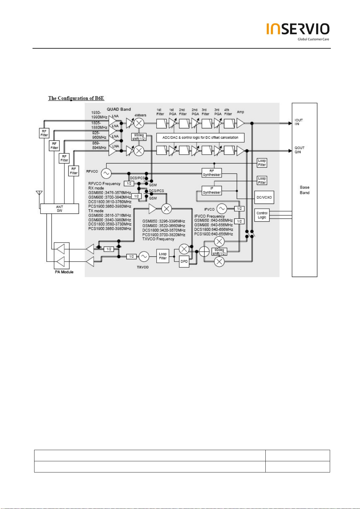
5 Radio Part
The radio part is realizes the conversion of the GMSK-HF-signals from the antenna to the
baseband and vice versa.
In the receiving direction, the signals are split in the I- and Q-component and led to the D/A-
converter of the logic part. In the transmission direction, the GMSK-signal is generated in an
Up Conversion Modulation Phase Locked Loop by modulation of the I- and Q-signals which
were generated in the logic part. After that the signals are amplified in the power amplifier.
Transmitter and Receiver are never active at the same time. Simultaneous receiving in the
GSM850/EGSM900 and GSM1800/GSM1900 band is impossible. Simultaneous
transmission in the GSM850/EGSM900 and GSM1800/GSM1900 band is impossible, too.
However the monitoring band (monitoring timeslot) in the TDMA-frame can be chosen
independently of the receiving respectively the transmitting band (RX- and TX timeslot of
the band).
EF51 RF-part is dimensioned for triple band operation (EGSM900, DCS1800, PCS19000)
supporting GPRS functionality up to multiclass 10.
The RF-circuit consists of the following components:
•Renesas Bright 5PL chip set (HD155153NP) with the following functionality:
PLL for local oscillator LO1 and LO2 and TxVCO
Integrated local oscillators LO1, LO2 (without loop filter)
Integrated TxVCO (without loop filter and core inductors for GSM)
Direct conversion receiver including LNA, DC-mixer, channel filtering and
PGC-amplifier
Active part of 26 MHz reference oscillator
Integrated Polar Loop, phase and amplitude control of transmitted output
power
•Renesas LTCC transmit PA PF09026B (incl. integrated power control circuitry for
GMSK mode)
•Frontend-Module including RX-/TX-switch and EGSM900 / DCS1800 / PCS 1900
receiver SAW-filters
•Crystal and passive circuitry of the 26MHz VCXO reference oscillator
Technical Documentation Release 1.0
TD_Repair_L3 _Theory of Operation_EF51_R1.0.pdf Page 12 of 55
Created by inservio GmbH for BenQ mobile GmbH & Co. OHG - Company Confidential2006©inservio
5.1 Block diagram RF part
Technical Documentation Release 1.0
TD_Repair_L3 _Theory of Operation_EF51_R1.0.pdf Page 13 of 55
Created by inservio GmbH for BenQ mobile GmbH & Co. OHG - Company Confidential2006©inservio
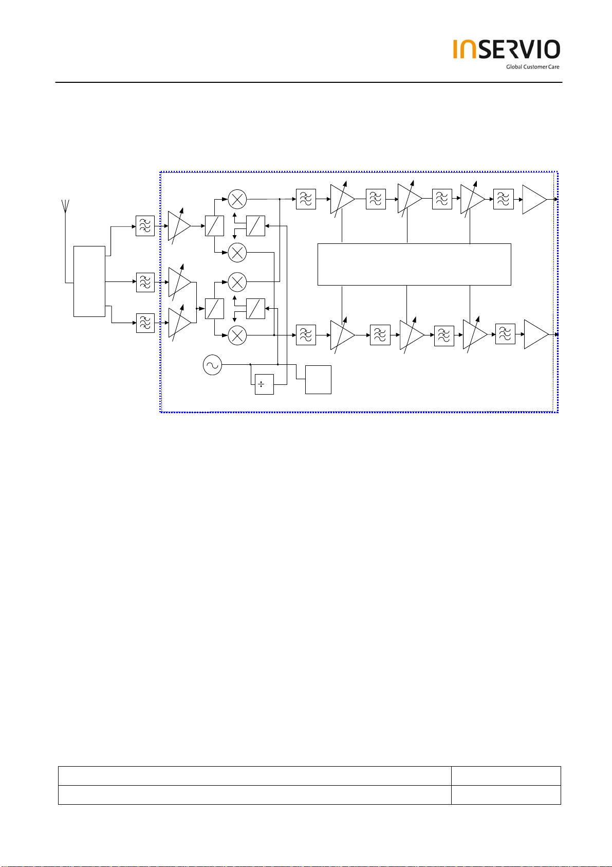
5.2 Receiver Operation
90
0
90
0
90
0
90
0
IRxP
IRxN
GSM LNA
DCS LNA
RX GSM: 925~960 MHz
DCS:
1805~1880 MHz
2
DCS:3610~3760 MHz
GSM:3700~3840 MHz
Shift(1/2)
Shift(1/2)
ADC/DAC & Control Logic for DC Offset Cancellation
RF
Synth
DCS:
1805~1880 MHz
PCS LNA
RFVCO
PCS:3860~3980 MHz
T/R
Switch
PCS:
1930~1990 MHz
GSM:
1850~1920 MHz
PCS:
1930~1990 MHz
QRxP
QRxN
HD155165BP (B6E)
The HD155165BP receiver is based upon the HD155155NP direct conversion design. As
HD155165BP supports quad band, the front end incorporates four LNAs and mixers. The
incoming RF signals are mixed directly down to I/Q base-band by the front-end block. This
incorporates four LNAs / four buffers and Gilbert Cell mixer blocks optimized for operation at
850MHz, 900MHz, 1800MHz, 1900MHz respectively.
The front-end block is followed by two closely matched base-band amplifier chains. These
include distributed low pass filter, three switched gain stages and one fixed gain stage. In
addition, the base-band section integrates A/D and D/A converters which provide automatic
on-chip correction of DC offsets. The three switched gain stages in each channel are DC
coupled and provide 90dB gain control range with 2dB step size. The first PGA has a
voltage gain range (x8-x1) with 6dB steps. The second PGA has a gain range (x8-x0.125)
with 2dB steps. The third PGA has a gain range (x8-x0.125) with 2dB steps. The final fixed
gain amplifier provides a gain of x3 or x6. The gain is set to match the on-chip levels to the
input dynamic range of the base-band. The base-band filtering in each channel comprises a
single RC low pass filter at the input of the first switched gain stage and three 2nd order
Butterworth filters, one at the input of each of the other switched gain stages. The R/C filter
requires an off-chip capacitor for each channel. The Butterworth filters are fully integrated
on-chip.
The base-band PGA includes a DC offset cancellation system. The auto calibration system
uses a successive approximation technique and requires around 20us to perform a three
stages calibration. The system calibrates out the offsets arising in both I and Q receives
channels.

Technical Documentation Release 1.0
TD_Repair_L3 _Theory of Operation_EF51_R1.0.pdf Page 14 of 55
Created by inservio GmbH for BenQ mobile GmbH & Co. OHG - Company Confidential2006©inservio
5.3 Transmitter Operation
Quad-Band PA
T/R
Switch Charge
Pump PFD
2
QTxP
QTxN
ITxP
ITxN
80/82 MHz
TX GSM: 880~ 915 MHz
DCS:1710~1785 MHz
Loop Filter
2
DCS:3580~3730 MHz
GSM:3840~3980 MHz
RFVCO
RF
Synth
IFVCO
I&Q Mod
90
0
Shift(1/2)
IF
Synth
2
2
DCS/
PCS
GSM DCS:1790~1865 MHz
GSM: 960~995 MHz
640/656 MHz
PCS:3860~3980 MHz
PCS:1930~1990 MHz
PCS:1850~1910 MHz
HD155165BP (B6E)
The B6E generates a modulated signal at IF with a quadrature modulator and converts it to
final frequency with an Offset Phase Locked Loop (OPLL).
The Offset Phase Locked Loop is simply a PLL with a down conversion mixer in the
feedback path. Using a down converter in the feedback path acts as an up-converter in the
forward path. This allows the output frequency to be different from the comparison
frequency without affecting the normal operation of the loop. Phase/frequency changes in
the reference signal are not scaled, as they would be if a divider were used in the feedback
path, hence the modulation is faithfully reproduced at the final frequency.
The main advantage of the OPLL in this application is that it forms a tracking band pass
filter around the modulated signal. This is because the loop cannot respond to phase
variations at the reference that are outside its closed loop bandwidth. Thus the broad band
phase noise from the quadrature modulator is shaped by the frequency response of the
closed loop allowing the TX noise specification to be met without further filtering.
A secondary advantage of the OPLL is that the output signal, coming from a VCO, is truly
constant envelope. This removes the problem of spectral spreading caused by AM to AM
and AM to PM conversion in the power amplifier.
The OPLL is formed from an on chip Gilbert cell down converter, limiter and phase detector
with on chip passive loop filter. The phase detector is implemented as a Gilvert cell with
current source output stage. The current output allows an integrator to be included in the
passive loop filter. This is similar to the technique commonly used in PLL synthesizers. A
digital phase detector is used to speed OPLL locking. After locking, the digital phase
detector is switched off and the analogue phase detector becomes active.

Technical Documentation Release 1.0
TD_Repair_L3 _Theory of Operation_EF51_R1.0.pdf Page 15 of 55
Created by inservio GmbH for BenQ mobile GmbH & Co. OHG - Company Confidential2006©inservio
5.4 Frequency generation
DCXO Operation
HD155165BP provides a DCXO function. With that function, we can build a reference
clock generation circuits as shown in the above graph. This means that the VCTCXO
module is not necessary for clock application, and only one crystal with 8ppm tolerance
and one varactor are enough.
The transistor in HD155165BP and two internal capacitors (C1, C2) provide a negative
resistance, and the crystal (X1) combined with some other passive components to provide
a positive resistance. When these two resistance values equal to each other at some
frequency, the oscillation will happen at that frequency. In our design target, the oscillation
frequency should be within 26MHz +/-15 ppm at least.
C2
C1
X1
+R -R

Technical Documentation Release 1.0
TD_Repair_L3 _Theory of Operation_EF51_R1.0.pdf Page 16 of 55
Created by inservio GmbH for BenQ mobile GmbH & Co. OHG - Company Confidential2006©inservio
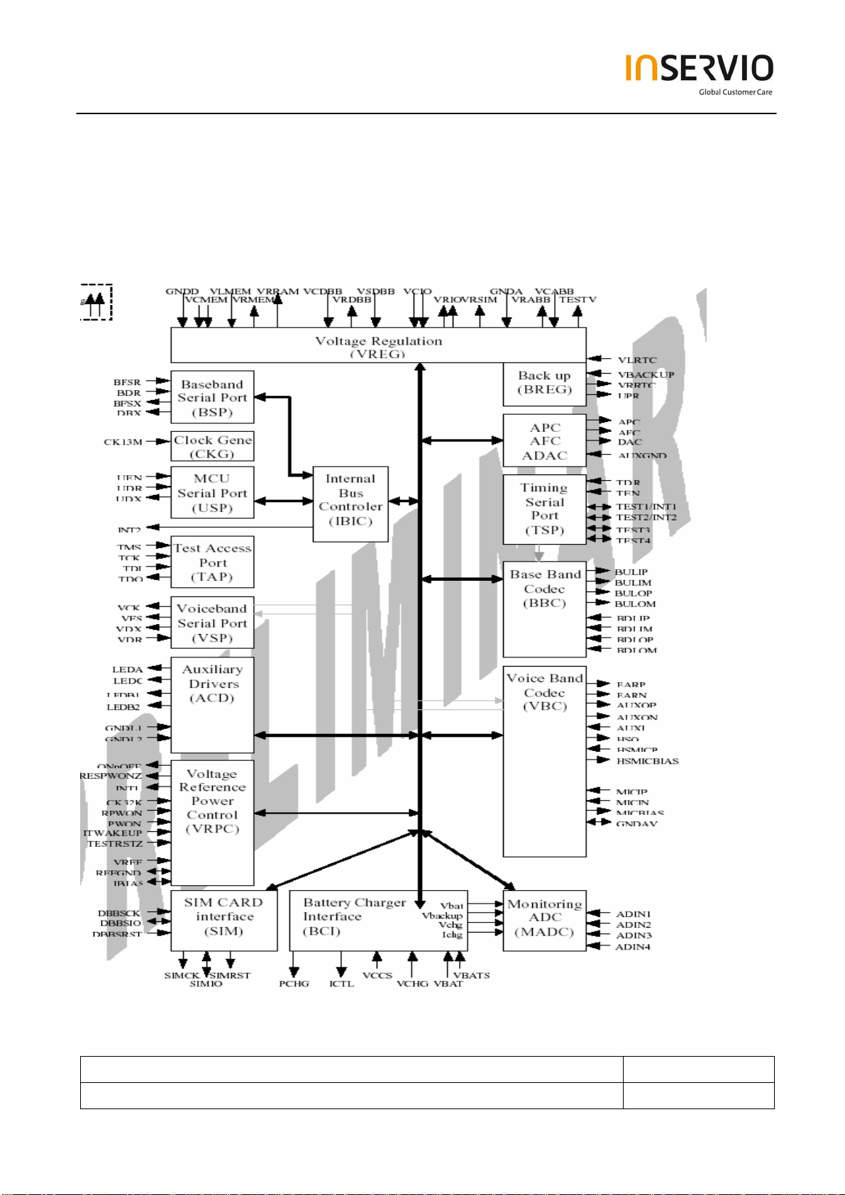
6 Logic / Control
6.1 Overview Hardware Structure
Introduction:
Pandora B2 utilizes TI’s chipsets (CALYPSO and IOTA) and RENESAS’s chipset (SHJ2SL)
as base-band solution. Base-band is composed with three potions: Logic, Analog/Codec
and MMP. CALYPSO is a GSM/GPRS digital base-band logic solution included
microprocessor, DSP, and peripherals. IOTA is a combination of analog/codec solution and
power management which contain base-band codec, voice-band codec, several voltage
regulators and SIM level shifter etc. SHJ2SL is a multimedia solution included
microprocessor, DSP, internal memory, and interrupt controller. In addition, Pandora B2
integrates with other features such as CMOS DSC module, Mini-SD card, vibration, melody
and charging etc. The following sections will present the operation theory with circuitry and
descriptions respectively.
6.2 Block Diagram
Technical Documentation Release 1.0
TD_Repair_L3 _Theory of Operation_EF51_R1.0.pdf Page 17 of 55
Created by inservio GmbH for BenQ mobile GmbH & Co. OHG - Company Confidential2006©inservio
6.3 CALYPSO (HERCROM400 )
Technical Documentation Release 1.0
TD_Repair_L3 _Theory of Operation_EF51_R1.0.pdf Page 18 of 55
Created by inservio GmbH for BenQ mobile GmbH & Co. OHG - Company Confidential2006©inservio

Technical Documentation Release 1.0
TD_Repair_L3 _Theory of Operation_EF51_R1.0.pdf Page 19 of 55
Created by inservio GmbH for BenQ mobile GmbH & Co. OHG - Company Confidential2006©inservio
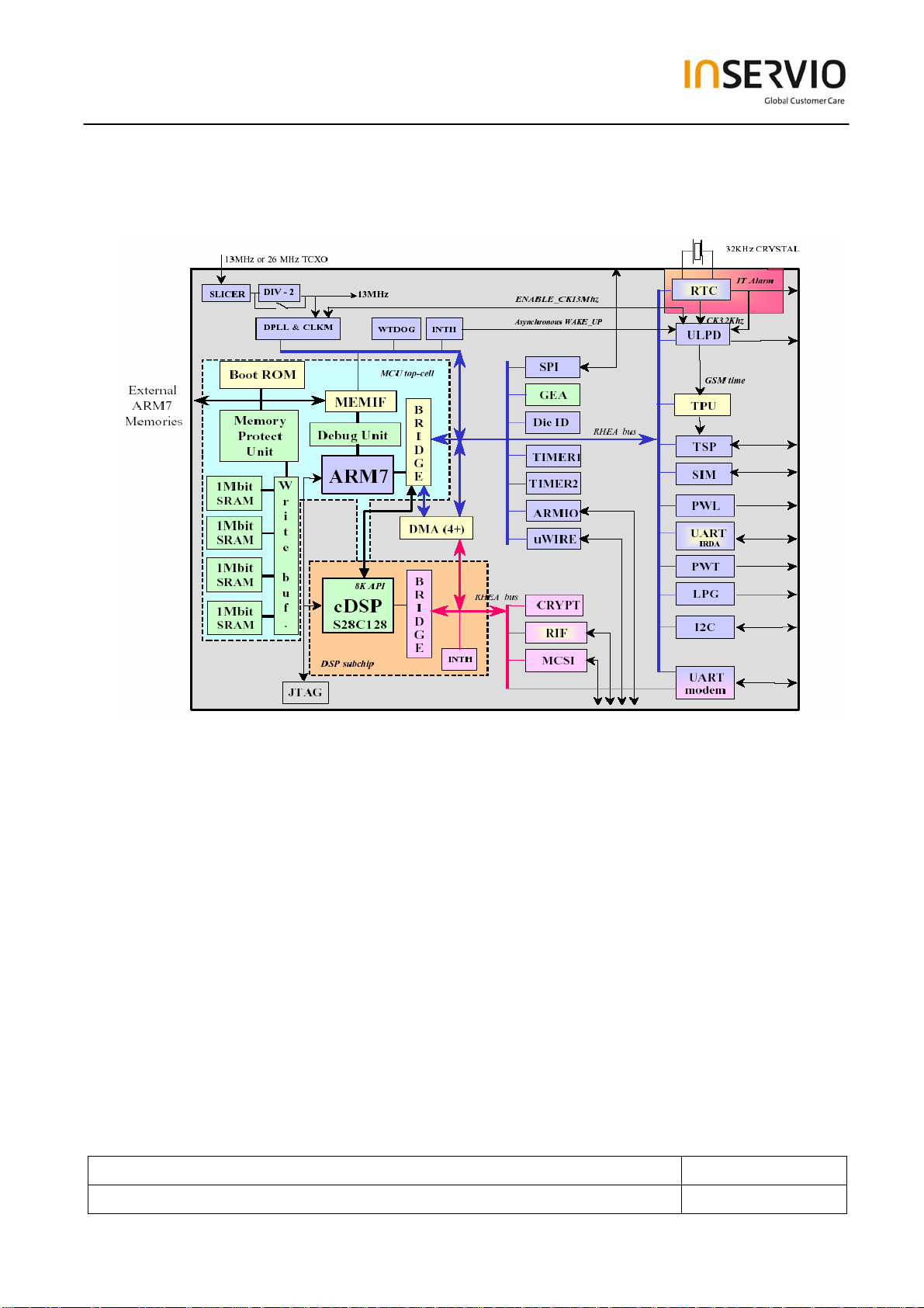
6.4 Calypso
CALYPSO (HERCROM400) is a chip implementing the digital base-band processor of a
GSM/GPRS mobile phone. This chip combines a DSP sub-chip (LEAD2 CPU) with its
program and data memories, a Micro-Controller core with emulation facilities (ARM7TDMIE)
and an internal 4M-bit RAM memory, a clock squarer cell, several compiled single-port or 2-
ports RAM and CMOS gates.
Major functions of this chip are as follows:
6.4.1 Real Time Clock (RTC)
T
2
3
4
T
T
I
I
he RTC block is an embedded RTC module fed with an external 32.768KHz Crystal.
Its basic functions are:
1. Time information (seconds/minutes/hours)
. Calendar information (Day/Month/Year/ Day of the week) up to year 2099
. Alarm function with interrupts (RTCINT is generated to wake up ABB)
. 32KHz oscillator frequency gauging
6.4.2 Pulse Width Light (PWL)
This module allows the control of the backlight of LCD and keypad by employing a 4096 bit
random sequence.
6.4.3 MODEM-UART
his UART interface is compatible with the NS 16C750 device which is devoted to the
connection to a MODEM through a standard wired interface. The module integrates two 64
words (9 and 11 bits) receive and transmit FIFOs which trigger levels are programmable. All
modem operations are controllable either via a software interface or using hardware flow
control signals. In Hyperion B1, we implement software flow control by only two signals:
TXD and RXD.
6.4.4 I2C master serial interface (I2C)
The I2C (Philips standard) is a half-duplex serial port using 2 lines (data and clock) for
data transmission with software addressable external devices. In Hyperion B1, we employ
I2C bus to control CLI in Audio Codec.
he I2C signals are defined as follows:
2C_SCL: programmed to the fast transmission mode (400KHz)
2C_SDA: the serial bi-directional data of the Audio Codec controller

Technical Documentation Release 1.0
TD_Repair_L3 _Theory of Operation_EF51_R1.0.pdf Page 20 of 55
Created by inservio GmbH for BenQ mobile GmbH & Co. OHG - Company Confidential2006©inservio
6.4.5 General Purposes I/O (GPIO)
Calypso provides 16 GPIOs configurable in read or write mode by internal registers. In
Hyperion B1, we utilize all of them as follows:
IO0: Let MMP power-on reset; ‘Low active’
IO1: Enable LCD back light; ‘H’:
enable, ‘L’:
disable
IO2: Control MMP’s MFI mode; ‘H’:
68-type mode, ‘L’:
80-type mode
IO3: Hall sensor INT
IO4: Hall sensor status; ‘L’:
close, ‘H’:
open
IO5: SIM power control
IO6: Accessory detect; ’H’:
no accessory, ’L’:
accessory in
IO7: Reset of external device: For Pandora B2, Reset for 3 combo memory and LCD
IO8: Indicates whether MMP is in software standby mode
IO9: I2C clock signal for FM
IO10: Detection of Mini-SD card; ‘H’:
No plugged in, ‘L’:
plugged in
IO11: BT power enable
IO12: I2C data signal for FM
IO13: INT request for MMP
IO14: SRAM high-byte enable
IO15: SRAM low-byte enable
6.4.6 Serial Port Interface (SPI)
The SPI is a full-duplex serial port configurable from 1 to 32 bits and provides 3 enable
signals programmable either as positive or negative edge or level sensitive. This interface
is working on 13MHz and is used for the GSM/GPRS baseband and voice A/D, D/A with
IOTA
6.4.7 Memory Interface and internal Static RAM
For external memory device (Flash and SRAM), this interface performs read and write
access with adaptation to the memory width. It also provides 6 chip-select signals
corresponding each to an address range of 8 mega bytes. One of these chip-select is
dedicated to the selection of an internal memory. In Hyperion B1, we employ nCS0/nCS1
(nCS0_NROM/nCS1_NROM) for external Flash and nCS2 (nCS2_NSRAM) for external
SRAM.
A 4Mbit SRAM is embedded on the die and memory mapped on the chip-select nCS6 of the
memory interface.
Other manuals for EF51
1
Table of contents
Other BenQ mobile Cell Phone manuals

BenQ mobile
BenQ mobile S88 Setup guide

BenQ mobile
BenQ mobile A38 User manual

BenQ mobile
BenQ mobile A38 User manual

BenQ mobile
BenQ mobile S75 User manual

BenQ mobile
BenQ mobile S88 User manual

BenQ mobile
BenQ mobile SL75 Setup guide

BenQ mobile
BenQ mobile S68 User manual

BenQ mobile
BenQ mobile M315 Setup guide

BenQ mobile
BenQ mobile EF51 User manual


