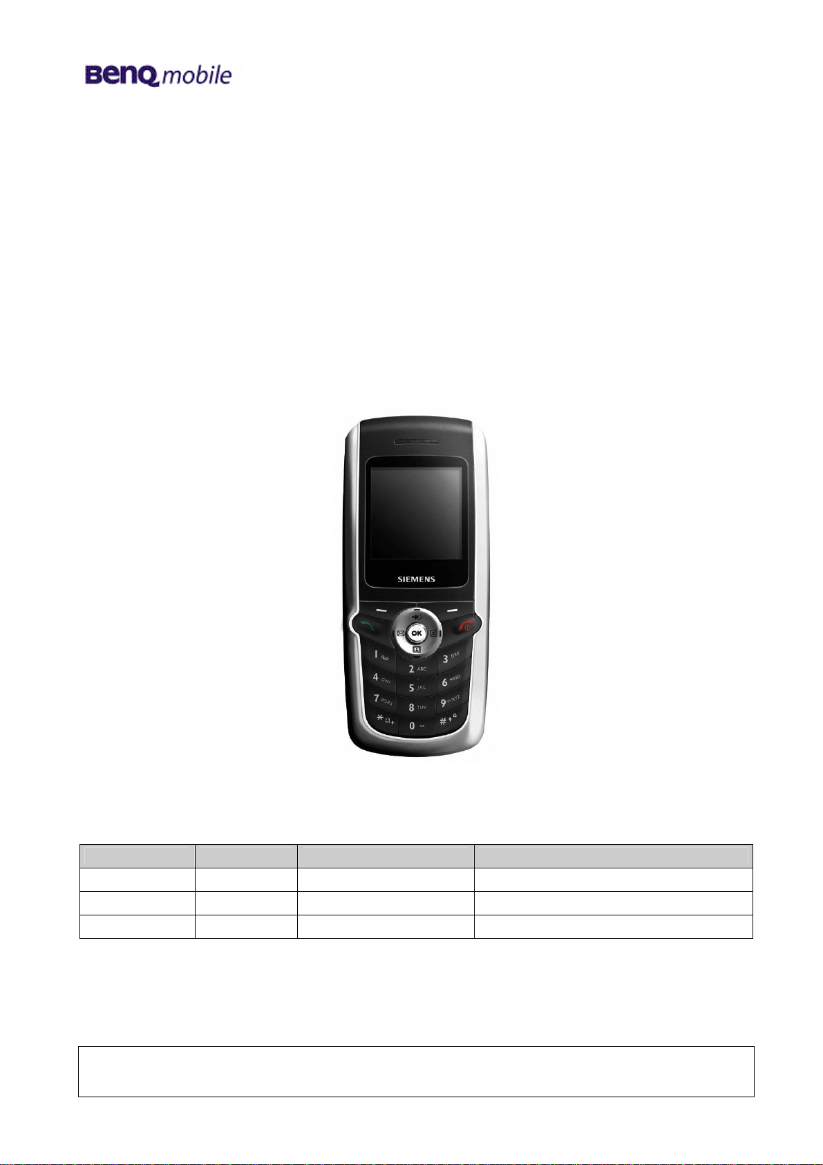
BenQ mobile M315 Setup guide
12/2005
Release 1.0
Technical Documentation
TD_Repair_L4 M315/AP75_R1.0.pdf Page 1 of 42
Service Repair Documentation
Level 4 (level 2,5e)
M315 / AP75
Release Date Department Notes to change
R 1.0 12.12.2005 BenQ Mobile (Taipei/KLF) New document

12/2005
Release 1.0
Technical Documentation
TD_Repair_L4 M315/AP75_R1.0.pdf Page 2 of 42
Table of Content
1Introduction ...............................................................................................................................3
1.1 PURPOSE...............................................................................................................................3
1.2 SCOPE ...................................................................................................................................3
1.3 TERMS AND ABBREVIATIONS ...................................................................................................3
2List of available level 4 (level 2,5e) parts ...............................................................................4
3Required Software for Level 4 (level 2,5e) ..............................................................................5
4Radio Part ..................................................................................................................................6
4.1 RECEIVER OPERATION............................................................................................................6
4.2 TRANSMITTER OPERATION......................................................................................................7
4.3 VCXO OPERATION.................................................................................................................8
4.4 BLUETOOTH OPERATION.........................................................................................................9
5Logic ( Base-Band ).................................................................................................................10
5.1 CALYPSO-LITE......................................................................................................................12
5.2 IOTA....................................................................................................................................15
5.3 POWER SUPPLY ...................................................................................................................19
5.3.1 System power on/off Sequence ...................................................................................21
5.4 MEMORY CIRCUIT .................................................................................................................22
5.5 LCD MODULE ( LCDM).........................................................................................................24
6Interfaces .................................................................................................................................27
6.1 AUDIO CIRCUIT .....................................................................................................................27
6.2 MELODY IC...........................................................................................................................29
6.3 AUDIO CIRCUIT .....................................................................................................................31
6.4 10 PINS I/O CONNECTOR......................................................................................................33
6.5 KEYPAD LED CIRCUIT...........................................................................................................35
6.6 VIBRATOR ............................................................................................................................36
6.7 SIM CIRCUIT ........................................................................................................................37
6.8 KEYPAD................................................................................................................................38
6.9 RTC CIRCUIT.......................................................................................................................40
7Charging circuit.......................................................................................................................41
12/2005
Release 1.0
Technical Documentation
TD_Repair_L4 M315/AP75_R1.0.pdf Page 3 of 42
1 Introduction
1.1 Purpose
This Service Repair Documentation is intended to carry out repairs on BenQ repair level 3-4.
1.2 Scope
This document is the reference document for all BenQ authorised Service Partners which are
released to repair Siemens mobile phones up to level 2.5.
1.3 Terms and Abbreviations

12/2005
Release 1.0
Technical Documentation
TD_Repair_L4 M315/AP75_R1.0.pdf Page 4 of 42
2 List of available level 4 (level 2,5e) parts
(according to Component Matrix V1.xx - check C-market for updates)
Product ID Order Number Description CM
M315
M315
M315
M315
M315
M315
M315
M315
M315
M315
M315
M315
M315
M315
M315
M315
M315
M315
M315
M315
M315
M315
M315
M315
M315
M315
M315
M315
M315
M315
M315

12/2005
Release 1.0
Technical Documentation
TD_Repair_L4 M315/AP75_R1.0.pdf Page 5 of 42
Required Equipment for Level 4 (level 2,5e)
GSM-Tester (CMU200 or 4400S incl. Options)
PC-incl. Monitor, Keyboard and Mouse
Adapter cable for Bootadapter (F30032-xx-A1)
Troubleshooting Frame M315_AP75 (F30032-xx-A1)
Power Supply
Spectrum Analyser
Active RF-Probe incl. Power Supply
Oscilloscope incl. Probe
RF-Connector (N<>SMA(f))
Power Supply Cables
Dongle (F30032-xx-A1)
BGA Soldering equipment
Reference: Equipment recommendation V1.6
(downloadable from the technical support page)
3 Required Software for Level 4 (level 2,5e)
Windows XP
XCSD Tools Level 2
GRT Version 3 or higher
Internet unblocking solution (JPICS)

12/2005
Release 1.0
Technical Documentation
TD_Repair_L4 M315/AP75_R1.0.pdf Page 6 of 42
4 Radio Part
M315 / AP75 utilizes TI’s chipsets (CALYPSO-Lite and IOTA) as base-band solution. Base-band is
composed with two potions: Logic and Analog/Codec. CALYPSO-Lite is a GSM/GPRS digital base-
band logic solution included microprocessor, DSP, and peripherals. IOTA is a combination of
analog/codec solution and power management which contain base-band codec, voice-band codec,
several voltage regulators and SIM level shifter etc. In addition, 56E22 integrates with other
features such as LED backlight, color LCD display, DSC, vibration, melody tone and charging etc.
The following sections will present the operation theory with circuitry and descriptions respectively.
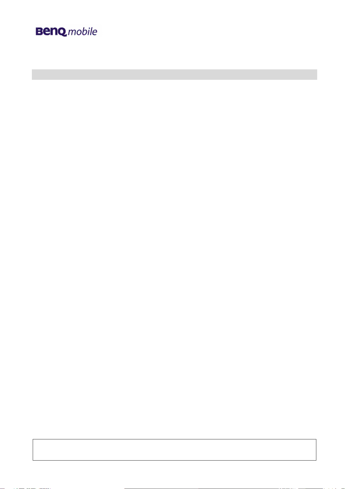
4.1 Receiver Operation
90
0
90
0
90
0
90
0
IRxP
IRxN
GSM LNA
DCS LNA
RX GSM: 925~960 MHz
DCS:
1805~1880 MHz
2
DCS:3610~3760 MHz
GSM:3700~3840 MHz
Shift(1/2)
Shift(1/2)
ADC/DAC & Control Logic for DC Offset Cancellation
RF
Synth
DCS:
1805~1880 MHz
PCS LNA
RFVCO
PCS:3860~3980 MHz
T/R
Switch
PCS:
1930~1990 MHz
GSM:
1850~1920 MHz
PCS:
1930~1990 MHz
QRxP
QRxN
The Receiver structure in HD155155NP is a zero-IF solution. That means RF signal is directly down-
converted to the baseband signal. And by the way, all of the DC-offset canceling processes
are done within chip. We do not have to care about that.
The LNA amplifies the RF signal after passing the T/R switch and RF SAW filter and before it enters
the down-converter section. The RF signal is mixed with a local oscillator (LO) signal to generate the
baseband signal.
Three LPFs are used in the baseband signal processing for reducing blocking signals. The first LPF
employs two external capacitors, and we can check whether the front-end (LNA + Mixer) is
functionally well or not by probing these two capacitors to see if there is any baseband
signal(<200kHz).
After three stages of DC-offset cancelling, the signal (I+/I-/Q+/Q-) then output to the baseband IC for
further processing.
12/2005
Release 1.0
Technical Documentation
TD_Repair_L4 M315/AP75_R1.0.pdf Page 7 of 42
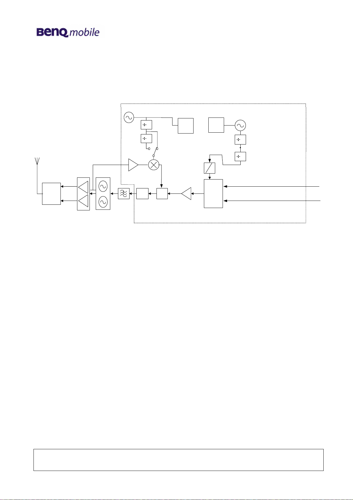
4.2 Transmitter Operation
Quad-Band PA
T/R
Switch Charge
Pump PFD
2
QTxP
QTxN
ITxP
ITxN
80/82 MHz
TX GSM: 880~ 915 MHz
DCS:1710~1785 MHz
Loop Filter
2
DCS:3580~3730 MHz
GSM:3840~3980 MHz
RFVCO
RF
Synth
IFVCO
I&Q Mod
90
0
Shift(1/2)
IF
Synth
2
2
DCS/
PCS
GSM DCS:1790~1865 MHz
GSM: 960~995 MHz
640/656 MHz
PCS:3860~3980 MHz
PCS:1930~1990 MHz
PCS:1850~1910 MHz
The transmitter chain converts differential IQ baseband signals to a suitable format for
transmission by a power amplifier.
The common mode voltage range of the modulator inputs is 1.05 V to 1.45 V and they have 2.0 Vpp
differential swing. The modulator circuit uses double-balanced mixers for the I and Q paths. The
Local signals are generated by dividing the IFLO signals by 8 in GSM band and by 4 in DCS band,
and then passed to the modulator through a phase splitter / shifter. The IF signals generated are
then summed to produce a single modulated IF signal which is amplified and fed into the offset PLL
block.
Within the offset PLL block there are a down converter, a phase comparator and a VCO driver. The
down converter mixes the first local signal and the TXVCO signal to create a reference local signal
for use in the offset PLL circuit. The phase comparator and the VCO driver generate an error
current, which is proportional to the phase differential between the reference IF and the modulated
IF signals. This current is
used in a third order loop filter to generate a voltage, which in turn modulates the TXVCO.
The RF signal is then amplified by PA and power control loop to the assigned power level within the
burst ramping mask. After passing the LPF of the T/R switch, the signal is then radiated through the
antenna.

12/2005
Release 1.0
Technical Documentation
TD_Repair_L4 M315/AP75_R1.0.pdf Page 8 of 42
4.3 VCXO Operation
+R-R
HD155155NP provides a VCXO function. With that function, we can build a reference clock
generation circuits as shown in the above graph. This means that the VCTCXO module is not
necessary for clock application, and only one crystal with 8ppm tolerance and one variocap are
enough.
The transistor in HD155155NP and two internal capacitors (C1, C2) provide a negative
resistance, and the crystal (X1) combined with some other passive components (including
variocap r : D1) to provide a positive resistance. When these two resistance values equal to each
other at some frequency, the oscillation will happen at that frequency. In our design target, the
oscillation frequency should be within 26MHz +/-15 ppm.
12/2005
Release 1.0
Technical Documentation
TD_Repair_L4 M315/AP75_R1.0.pdf Page 9 of 42
4.4 Bluetooth Operation
2402~2480 MHz
BC3-Handphone
LDO
2.8V
VBAT
SPI Interface
G2-lite
IRDA
UART
MCSI
B5E-VCXO
26MHz
INTERRUPT
CLK_SEL OR
Gate TCXOEN
The Bluetooth main chip – BC3-Handphone deals with BT RF signal from chip antenna and
baseband signal from G2-lite including down/up-converting, de/- modulation and de/- coding … The
BC3-Handphone could accept clock frequency from 8MHz to 40MHz. In our application, we feed the
chip with 26MHz clock from RF chip, HD155155N, and share with G2-lite by an OR-Gate. So GSM
part and BT part could go to sleep respectively. BC3-Handphone could wake G2-lite up by a
interrupt. The BC3-Handphone is controlled by AT commands that come from G2-lite via IRDA
UART. The Data between BC3-Handphone and G2-lite are transmitted and received via MCSI
interface. The SPI interface is reserved for firmware downloading for BT chip of Flash-type. The
power BT chip needed outside is 2.8V the same with voltage level of I/O interface of G2-lite.

12/2005
Release 1.0
Technical Documentation
TD_Repair_L4 M315/AP75_R1.0.pdf Page 10 of 42
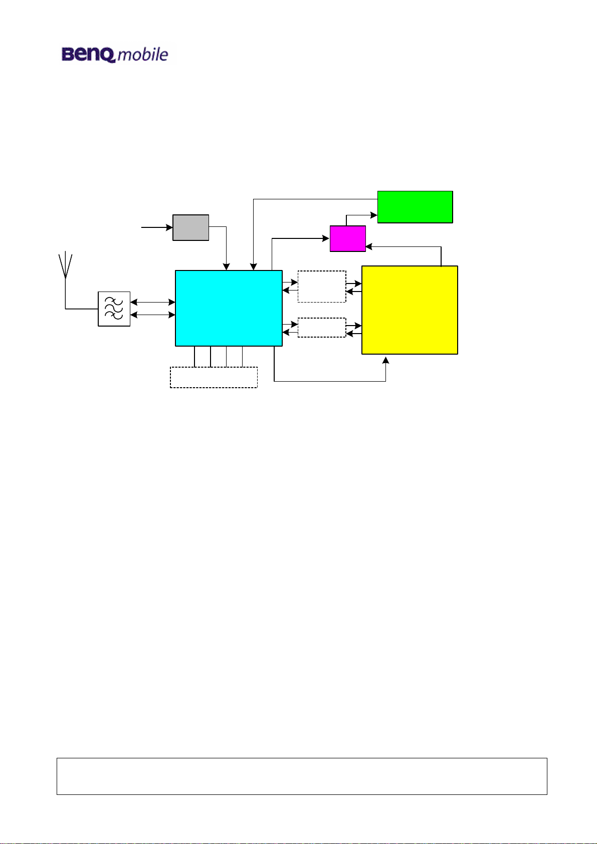
5 Logic ( Base-Band )
Introduction:
56E22 utilizes TI’s chipsets (CALYPSO-Lite and IOTA) as base-band solution. Base-band is
composed with two potions: Logic and Analog/Codec. CALYPSO-Lite is a GSM/GPRS digital
base-band logic solution included microprocessor, DSP, and peripherals. IOTA is a combination
of analog/codec solution and power management which contain base-band codec, voice-band
codec, several voltage regulators and SIM level shifter etc. In addition, 56E30 integrates with
other features such as LED backlight, color LCD display , DSC, vibration, melody tone and
charging etc. The following sections will present the operation theory with circuitry and
descriptions respectively.
Block Diagram CPU CALYPSO (HERCROM40 )
12/2005
Release 1.0
Technical Documentation
TD_Repair_L4 M315/AP75_R1.0.pdf Page 11 of 42
IOTA

12/2005
Release 1.0
Technical Documentation
TD_Repair_L4 M315/AP75_R1.0.pdf Page 12 of 42
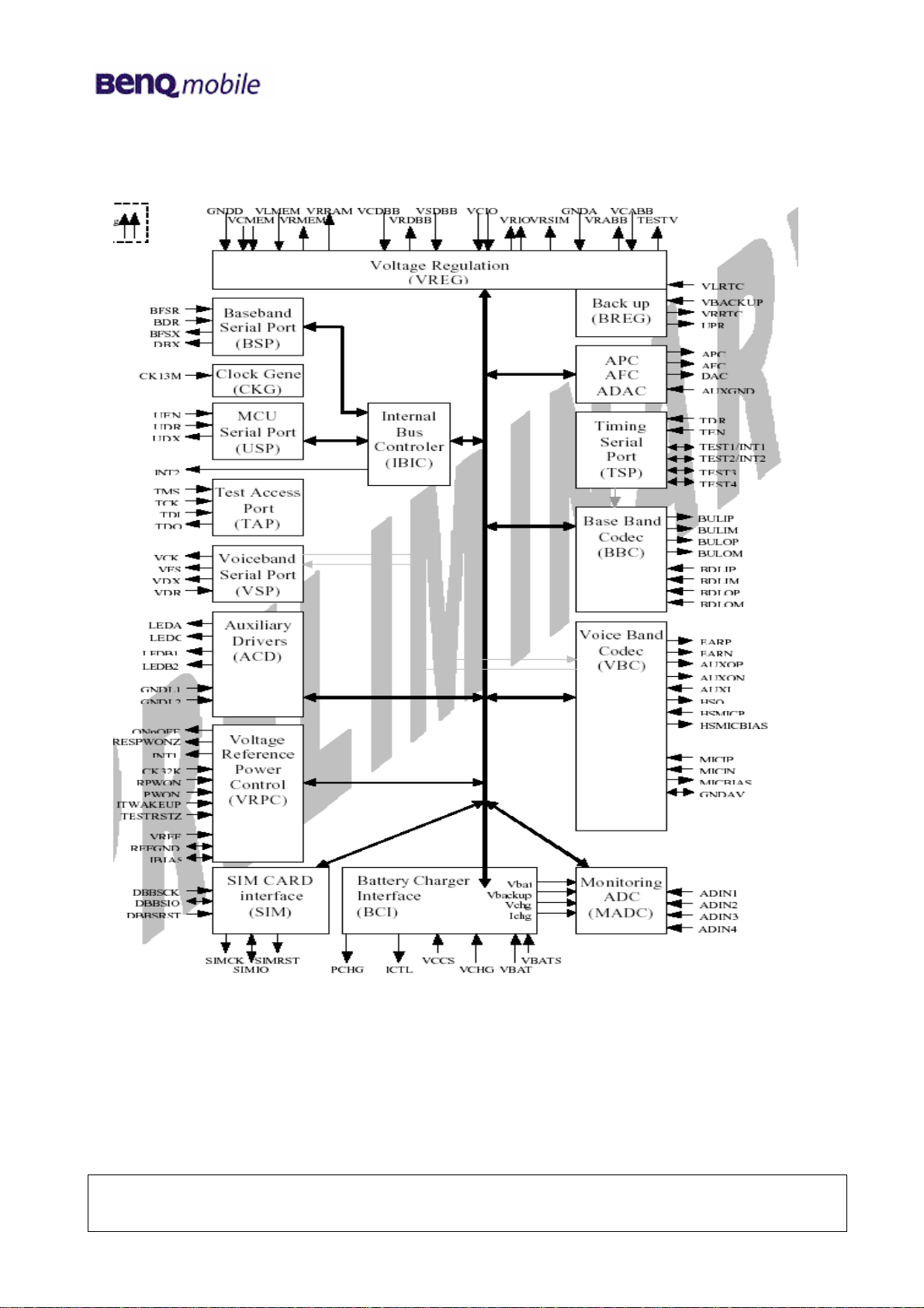
5.1 Calypso-Lite
CALYPSO-Lite (HERCROM400) is a chip implementing the digital base-band processor of a
GSM/GPRS mobile phone. This chip combines a DSP sub-chip (LEAD2 CPU) with its program
and data memories, a Micro-Controller core with emulation facilities (ARM7TDMIE) and an
internal 2M-bit RAM memory, a clock squarer cell, several compiled single-port or 2-ports RAM
and CMOS gates.
Major functions of this chip are as follows:
Real Time Clock (RTC)
The RTC block is an embedded RTC module fed with an external 32.768KHz Crystal. Its basic
functions are:
1. Time information (seconds/minutes/hours)
2. Calendar information (Day/Month/Year/ Day of the week) up to year 2099
3. Alarm function with interrupts (RTCINT is generated to wake up ABB)
4. 32KHz oscillator frequency gauging
Pulse Width Light (PWL)
This module allows the control of the backlight of LCD and keypad by employing a 4096 bit
random sequence .In the 56E30, we use the LT/PWL function to turn on the keypad light LED.
MODEM-UART
This UART interface is compatible with the NS 16C750 device which is devoted to the
connection to a MODEM through a standard wired interface. The module integrates two 64
words (9 and 11 bits) receive and transmit FIFOs which trigger levels are programmable. All
modem operations are controllable either via a software interface or using hardware flow control
signals. In 56E30 , we implement software flow control by only two signals: TXD0 and RXD0.
General Purposes I/O (GPIO)
Calypso-Lite provides 16 GPIOs configurable in read or write mode by internal registers. In
56E30, we utilize 9 of them as follows , others are used in the dual function mode or N/A:
IO 0 : SPK_FM_HF
IO 1 : VOL_CLK
IO 2 : MELODY_INT
IO 3 : VOL_UpDown
IO 4 : FM_SPK

12/2005
Release 1.0
Technical Documentation
TD_Repair_L4 M315/AP75_R1.0.pdf Page 13 of 42
IO 5 : X
IO 6 : ACCESSORY_IN
IO 7 : NRESET_OUT
IO 8 :
IO 9 : NLED_DRIVE_SD
IO 10 : FM_EN
IO 11 : FM_SCL
IO 12 : FM_SDA
IO 13 :
IO14: SRAM high-byte enable
IO15: SRAM low-byte enable
Serial Port Interface (SPI)
The SPI is a full-duplex serial port configurable from 1 to 32 bits and provides 3 enable signals
programmable either as positive or negative edge or level sensitive. This interface is working on
13MHz and is used for the GSM/GPRS baseband and voice A/D, D/A with IOTA
Memory Interface and internal Static RAM
For external memory device (Flash and SRAM), this interface performs read and write access
with adaptation to the memory width. It also provides 6 chip-select signals corresponding each
to an address range of 8 mega bytes. One of these chip-select is dedicated to the selection of
an internal memory. In 56E30, we employ nCS0 (NROM_CS0) for external 64 Mbits Flash and
nCS1 (NRAM_CS1) for external 16Mbits SRAM. A 2Mbit SRAM is embedded on the die and
memory mapped on the chip-select nCS6 of the memory interface .The access cycle is
guaranteed with 0 wait-state for any cycle frequency up to 39MHz. About others chip selects
allocation are nCS2 (NDSCM_CS2) for DSC backend IC and nCS3 (NLCDM_CS3) for LCDM
driver and nCS4 for melody IC ..
SIM Interface
The Subscriber Identity Module interface will be fully compliant with the GSM 11.11 and ISO/IEC
7816-3 standards. Its external interface is 3 Volts only. 5 Volts adaptation will be based on
external level shifters.
JTAG
In 56E30, JTAG is used for software debugging.

12/2005
Release 1.0
Technical Documentation
TD_Repair_L4 M315/AP75_R1.0.pdf Page 14 of 42
Time Serial Port (TSP)
The TPU is a real-time sequencer dedicated to the monitoring of GSM/GPRS baseband
processing. The TSP is a peripheral of the TPU which includes both a serial port (32 bits) and a
parallel interface. The serial port can be programmed by the TPU with a time accuracy of the
quarter of GSM bit. The serial port is uni-directional (transmit only) when used with IOTA. The
serial port provides 4 enable signals programmable either as positive or negative edge or level
sensitive. This serial port is derived from 6.5MHz and used to control the real time GSM windows
for the baseband codec and the windows for ADC conversion.
TSP Parallel interface (ACT)
The parallel interface allows control 13 external individual outputs and 1 internal signal with a
time accuracy of the quarter of GSM bit. These parallel signals are mainly used to control the RF
activity. In 56F05, we employ 5 of them to control RF activity.
TSPACT1: GSM_T/R
TSPACT2: DCS_T/R
TSPACT3: PCS_RX
TSPACT6: TX_ON
TSPACT9: Band Select
TSPACT10: Latch enable
Radio Interface (RIF)
The RIF (Radio Interface) Module is a buffered serial port derived from the BSP peripheral
module of the defined for TMS320C5X. The external serial data transmission is supported by a
full-duplex double-buffered serial port interface. The interface is used for transfer of baseband
transmit and receive data and also to access all internal programmation registers of the device.
Miscellaneous:
Some important Baseband /RF interface signals are defined as follows:
CLKTCXO: 13MHz VTCXO Clock from RF circuit
TCXOEN: 13MHz VTCXO Clock Enable signal

12/2005
Release 1.0
Technical Documentation
TD_Repair_L4 M315/AP75_R1.0.pdf Page 15 of 42
5.2 IOTA
Together with a digital base-band device (Calypso-Lite), IOTA is part of a TI DSP solution
intended for digital cellular telephone applications including GSM 900, DCS 1800 and PCS 1900
standards (dual band capability).
It includes a complete set of base-band functions to perform the interface and processing of voice
signals, base-band in-phase (I) and quadrature (Q) signals which support single-slot and multi-
slot mode, associated auxiliary RF control features, supply voltage regulation, battery charging
control and switch ON/OFF system analysis. IOTA interfaces with the digital base-band device
through a set of digital interfaces dedicated to the main functions of Calypso-Lite, a base-band
serial port (BSP) and a voice-band serial port (VSP) to communicate with the DSP core (LEAD),
a micro-controller serial port to communicate with the micro-controller core and a time serial port
(TSP) to communicate with the time processing unit (TPU) for real time control.
IOTA also includes on chip voltage reference, under voltage detection and power-on reset
circuits.
Major functions of this chip are as follows:
Baseband Codec (BBC)
The baseband codec includes a two-channel uplink path and a two-channel downlink path.
The baseband uplink path (BUL) modulates the bursts of data coming from the DSP via the
baseband serial port (BSP) and to be transmitted at the antenna. Modulation is performed by a
GMSK modulator. The GMSK modulator implemented in digital technique generates In-phase (I)
and Quadrature (Q) components, which are converted into analog base-band by two 10 bits
DACs filters. It also includes secondary functions such as DC offset calibration and I/Q gain
unbalance.
The baseband downlink path (BDL) converts the baseband analog I & Q components coming
from the RF receiver into digital samples and filters these resulting signals through a digital FIR
to isolate the desired data from the adjacent channels. During reception of burst I & Q digital
data are sent to the DSP via the baseband serial port (BSP) at a rate of 270 KHz.
Automatic Frequency control (AFC)
The automatic frequency control function consists of a digital to analog converter optimized for
high resolution DC conversion. Its purpose is to control the frequency of the GSM 13MHz
oscillator to maintain mobile synchronization on the base station and allow proper transmission
and demodulation.

12/2005
Release 1.0
Technical Documentation
TD_Repair_L4 M315/AP75_R1.0.pdf Page 16 of 42
Automatic Power Control (APC)
Purpose of the Automatic Power Control (APC) is to generate an envelope signal to control the
power ramping up, ramping down and power level of the radio burst.
The APC structure is intended to support single slot and multi-slots transmission with smooth
power transition when consecutive bursts are transmitted at different power level. It includes a
DAC and a RAM in which the shape of the edges (ramp-up and ramp-down) of the envelope
signals are stored digitally. This envelope signal is converted to analog by a 10 bits digital to
analog converter. Timing of the APC is generated internally and depends of the real time signals
coming from the TSP and the content of two registers which control the relative position of the
envelope signal versus the modulated I & Q.
Time serial port (TSP)
Purpose of the time serial port is to control in real time the radio activation windows of IOTA
which are BUL power-on, BUL calibration, BUL transmit, BDL power-on, BDL calibration and BDL
receive and the ADC conversion start.
These real time control signals are processed by the TPU of DBB and transmitted serially to
ABB via the TSP, which consists in a very simple two pins serial port. One pin is an enable
(TEN) the other one the data receive (TDR). The master clock CK13M divided by 2 (6.5MHz) is
used as clock for this serial port.
Voice band Codec (VBC)
The VBC processes analog audio components in the uplink path and transmits this signal to DSP
speech coder through the voice serial port (VSP). In the downlink path the VBC converts the
digital samples of speech data received from the DSP via the voice serial port into analog audio
signal. Additional functions such as programmable gain, volume control and side-tone are
performed into the voice band codec.
Micro-controller serial port (USP)
The micro-controller serial port is a standard synchronous serial port. It consists in three
terminals, data transmit (UDX), data receive (UDR) and port enable (UEN). The clock signal is
13MHz clock. The USP receives and sends data in serial mode from and to the external micro-
controller and in parallel mode from and to the internal GSM Baseband a Voice A/D D/A
modules. The micro-controller serial port allow read and write access of all internal registers
under the arbitration of the internal bus controller.

12/2005
Release 1.0
Technical Documentation
TD_Repair_L4 M315/AP75_R1.0.pdf Page 17 of 42
SIM card shifters (SIMS)
The SIM card digital interface in ABB insures the translation of logic levels between DBB and SIM
card, for transmission of 3 different signals; a clock derived from a clock elaborated in DBB, to the
SIM card (DBBSCKSIMCLK). a reset signal from DBB to the SIM card (DBBSRSTSIMRST),
and serial data from DBB to SIM card (DBBSIOSIMIO) and vice-vera.
The SIM card interface can be programmed to drive a 1.8V and 3 V SIM card
Voltage Regulation (VREG)
Linear regulation is performed by several low dropout (LDO) regulators to supply analog and
digital baseband circuits.
(1) LDO VRDBB generates the supply voltage (1.85V, 1.5V,and 1.35V) for the digital core of
DBB. In 56E30, it is programmed to 1.5V. This regulator takes power from the battery
voltage
(2) LDO VRABB generates the supply voltage 2.8V for the analog function of ABB. It is
supplied by the battery.
(3) LDO VRIO generates the supply voltage 2.8V for the digital core of ABB and digital I/O’s of
DBB and ABB. It is supplied from battery voltage.
(4) LDO VRMEM generates the supply voltages 2.8V for DBB memory interfaces I/O’s.
(5) LDO VRRAM generates the supply voltages 2.8V for DBB memory interfaces I/O’s
(6) LDO VRRTC generates the supply voltages (1.85,1.5, or 1.35V) and supply voltage 1.5V for
the following block of DBB (real time clock and 32K oscillator ). It’s supplied by UPR
(7) LDO VRSIM generates the supply voltages (1.8V, 2.9V) for SIM card interface I/O’s
Baseband Serial Port (BSP)
The BSP serial interface is used for both configuration of the GSM baseband and voice A/D D/A
(read and write operation in the internal registers), and transmission of the radio data to the DSP
during reception of a burst by the downlink part of the GSM baseband & voice A/D D/A. Four
pins are used by the serial port: BFSR and BDR for receive, BFSX and BDX for transmit. BDX is
the transmitted serial data output. BFSX is the transmit frame synchronization and is used to
initiate the transfer of the transmit data. BDR is the received serial input. BFSR is the receive
frame synchronization and is used to initiate the reception data.

12/2005
Release 1.0
Technical Documentation
TD_Repair_L4 M315/AP75_R1.0.pdf Page 18 of 42
Battery charger Interface (BCI)
The main function of the ABB charger interface is the charging control of either a 1-cell Li-ion
Battery or 3-serie Ni-MH cell batteries with the support of the micro-controller. The battery
monitoring uses the 10 bit ADC converter from the MADC to measure the battery voltage, battery
temperature, battery type, battery charge current, battery charger input voltage. The magnitude
of the charging current is set by the 10 bits of a programming register converted by an 10 bit
Digital to Analog Converter, whose output sets the reference input of the charging current control
loop. The battery charger interface performs also some auxiliary functions. They are battery pre-
charge, battery trickle charge and back-up battery charge if it is rechargeable.
Monitoring ADC (MADC)
The MADC consists in a 10-bit analog to digital converter combined with a nine inputs analog
multiplexer. Out of the nine inputs five are available externally, the four remaining being
dedicated to main battery voltage, back up battery voltage, charger voltage and charger current
monitoring. On the five available externally three are standard inputs intended for battery
temperature, battery type measurements.
Reference Voltage / Power on Control (VRPC)
An integrated band-gap generates a reference voltage. This reference is available on an external
pin for external filtering purpose only. This filtered reference is internally used for analog
functions. The external resistor connected between pin IBIAS and GNDREF sets, from the band-
gap voltage, the value of the bias currents of the analog functions. The VRPC block is in charge
to control the Power ON, Power OFF, Switch On, and Switch OFF sequences. Even in Switch
OFF state some blocks functions are performed. These “permanent” functions are functions,
which insure the wake-up of the mobile such as ON/OFF button detection or charger detection.
Interrupts are generated at power-down detection of the PWON button and when abnormal
voltage conditions are detected.
Internal bus and interrupt controller (IBIC)
Read and write access to all internal registers being possible via both the BSP and USP,
purpose of the internal bus controller is to arbitrate the access on the internal bus and to direct
the read data to the proper serial port. During reception of a burst the internal bus controller
assign the transmit part of the BSP to the base-band downlink to transfer the I & Q samples to
the DSP.
This block also handles the internal interrupts generated by the MADC, BCI and VRPC blocks
and generates the micro-controller interrupt signal INT2.
12/2005
Release 1.0
Technical Documentation
TD_Repair_L4 M315/AP75_R1.0.pdf Page 19 of 42
5.3 Power Supply
RSIM
1.8/2.9V
10mA
RRAM
1.8/2.8
50mA
RMEM
1.8/2.8V
60mA
RDBB
1.3/1.5/1.8V
120mA
ABB
D Igital
Core
I/O
ABB
Analog
Core
RSIM
1.8/2.9V
10mA
RABB
2.8V
50mA
BBS
ABB
VRPC Core
RIO
2.8V
100mA
SIM
CARD
SRAM
CORE
M enory
IO
CORE
DBB
Memories
I/O
DBB
COre
DBB
I/O
DBB Backup
RTC
I/O R T C
D B B S p lit P ow er
Low Power Domain
VBAT ABB
VCAM
VCMEM
VLMEN
VCDBB
VCIO1
VCIO2
VCABB
VBAT
BACK
UP
VRSIM
VRRAM
VRMEM
VSDBB
VRDBB
VRIO1
VRIO2
VRABB
VLRTC
VRRTC
Sel 1.8V
Sel 1.5V

12/2005
Release 1.0
Technical Documentation
TD_Repair_L4 M315/AP75_R1.0.pdf Page 20 of 42
Description:
The voltage regulators embedded in IOTA consists of seven sub blocks. Several low-dropout (LDO)
regulators perform linear voltage regulation. These regulators supply power to internal analog and
digital circuit, to DBB processor, and to external memory.
· LDO (VRDBB) is a programmable regulator that generates the supply voltages(1.8V,1.5V and
1.3V) for the core of the DBB processor. The main battery supplies VRDBB.
· LDO (VRIO) generate the supply voltage (2.8V) for the digital core and I/O of the TWL3014 device.
The main battery supplies VRIO.
· LDO (VRMEM) is a programmable regulator that generates the supply voltages (2.8V and 1.8V) for
external memories (typically flash memories) and DBB memory interface I/O. The main battery
supplies VRMEM.
· LDO (VRRAM) is a programmable regulator that generate the supply voltages (2.8V and 1.8V) the
external memory (typically SRAM memories) and DBB memory interface I/Os. The main battery
supplies VRRAM.
· LDO (VRABB) generates the supply voltage (2.8V) for the analog functions of the TWL 3014
devices. The main battery supplies VRABB.
· LDO (VRSIM) is a programmable regulator that generates the supply voltages (2.9V and 1.8V) SIM
card and SIM card devices. The main battery supplies VRSIM.
· LDO (VRTC) is a programmable regulator that generate the supply voltage (1.8V.1.5Vand 1.3V) for
real time clock and the 32-KHZ oscillator located in the DBB device during all modes. The main or
backup battery supplies VRTC.
This manual suits for next models
1
Table of contents
Other BenQ mobile Cell Phone manuals

BenQ mobile
BenQ mobile A38 User manual

BenQ mobile
BenQ mobile EF51 User manual

BenQ mobile
BenQ mobile SL75 Setup guide

BenQ mobile
BenQ mobile S68 User manual

BenQ mobile
BenQ mobile S88 User manual

BenQ mobile
BenQ mobile A38 User manual

BenQ mobile
BenQ mobile S88 Setup guide

BenQ mobile
BenQ mobile S75 User manual

BenQ mobile
BenQ mobile EF51 User manual


