BenQ mobile S88 Setup guide
Release 1.0
Technical Documentation
02/2006
TD_Repair_L3_Theory of Operation_S88_R1.0.pdf Page 1 of 54
Service Repair Documentation
Level 3 –S88
Release Date Department Notes to change
R 1.0 BenQ S CC CES New document
Company Confidential
2006©BenQ Mobile

Release 1.0
Technical Documentation
02/2006
TD_Repair_L3_Theory of Operation_S88_R1.0.pdf Page 2 of 54
Table of Content
1
Introduction ...............................................................................................................................4
1.1
P
URPOSE
...............................................................................................................................4
1.2
S
COPE
...................................................................................................................................4
1.3
T
ERMS AND
A
BBREVIATIONS
...................................................................................................4
2
List of available level 3 parts....................................................................................................5
3
Required Equipment for Level 3 ..............................................................................................7
4
Required Software for Level 3..................................................................................................7
5
PCB Main Board Overview .......................................................................................................8
6
Radio Part Introduction.............................................................................................................9
6.1
B
LOCK DIAGRAMS
RF
PART
...................................................................................................10
6.2
BRIGHT
VI
E
CHIPSET
(HD
155165BP) ...............................................................................11
6.2.1
First Local Oscillator.....................................................................................................11
6.2.2
RF-PLL .........................................................................................................................11
6.2.3
RF VCO (LO1)..............................................................................................................11
6.2.4
Second local oscillator (640~656MHz).........................................................................11
6.2.5
Receiver .......................................................................................................................12
6.2.6
Transmitter ...................................................................................................................12
6.2.7
Bright IC Overview .......................................................................................................13
6.3
A
NTENNA SWITCH
(
ELECTRICAL
/
MECHANICAL
).......................................................................14
6.4
RF
M
ICRO
D
EVICES TRANSMITTER POWER AMPLIFIER
RF3166 ..............................................15
7
Logic / Control Introduction...................................................................................................16
7.1
S88
L
OGIC
B
LOCK
D
IAGRAM
.................................................................................................16
7.2
C
ALYPSO
-
TWL3014 ...........................................................................................................17
7.2.1
Operation theory...........................................................................................................18
7.3
IOTA
–
TWL3025 ................................................................................................................21
7.3.1
Operation theory...........................................................................................................22
7.3.2
Power Supply diagram .................................................................................................26
7.3.3
System power on/off Sequence ...................................................................................27
7.4
A
PPLICATION
P
ROCESSOR
SHJ2
+
SD128............................................................................28
7.4.1
Multimedia Processor SH7315.....................................................................................29
Company Confidential
2006©BenQ Mobile

Release 1.0
Technical Documentation
02/2006
TD_Repair_L3_Theory of Operation_S88_R1.0.pdf Page 3 of 54
7.5
C
OMBO
M
EMORY
C
HIP
M6MGA157F2LCWG ......................................................................36
7.5.1
MMP Power—PMIC .....................................................................................................37
7.6
BC3-ROM ...........................................................................................................................38
7.7
10
PIN
I/O.............................................................................................................................38
7.8
T-FLASH
CARD
....................................................................................................................39
7.9
C
HARGING CIRCUIT
...............................................................................................................40
7.10
L
I
-
ION
/L
I
P
OLYMER
B
ATTERY
C
HARGER
ISL6262C................................................................41
7.11
A
UDIO
C
ODEC AND
A
UDIO AMPLIFIER
....................................................................................42
7.12
OLED
M
ODULE
....................................................................................................................46
7.13
C
AMERA MODULE
.................................................................................................................48
7.14
F
LASH
LED
DRIVER CIRCUIT
..................................................................................................50
7.15
K
EYPAD
LED
CIRCUIT
...........................................................................................................51
7.16
K
EYPAD
................................................................................................................................52
7.17
V
IBRATOR CIRCUIT
................................................................................................................54
Company Confidential
2006©BenQ Mobile
Release 1.0
Technical Documentation
02/2006
TD_Repair_L3_Theory of Operation_S88_R1.0.pdf Page 4 of 54
1 Introduction
1.1 Purpose
This Service Repair Documentation is intended to carry out repairs on BenQ repair level 3.
1.2 Scope
This document is the reference document for all BenQ authorised Service Partners which are
released to repair BenQ Mobile phones up to level 3.
1.3 Terms and Abbreviations
Company Confidential
2006©BenQ Mobile

Release 1.0
Technical Documentation
02/2006
TD_Repair_L3_Theory of Operation_S88_R1.0.pdf Page 5 of 54
2 List of available level 3 parts
Product Order Number Description CM
S88 L50634-Z97-C553 CONN DC PWR PA05302-QNJ BQ2B.13120.021
S88 L50634-Z97-C633 CONN AXK7L20227 BQ2K.L1096.020
S88 L50634-Z97-C634 CONN AXK7L30227 BQ2K.L1096.030
S88 L50634-Z97-C635 CONN AXK734245 BQ2K.L1165.034
S88 L50634-Z97-C636 CONN BF1-0115 BQ2K.L1235.010
S88 L50634-Z97-C554 CONN ANT RF05301-PG BQ2K.M0001.001
S88 L50634-Z97-C556 CONN BAT3PD2.5AB303Y-C0G1 BQ2K.N0080.001
S88 L50634-Z97-C558 CONN I/O 10P P0.5 BQ2K.N0081.001
S88 L50634-Z97-C637 CONN SIM BM05306-D18 BQ2K.N5030.011
S88 L50634-Z97-C638 CONN MEMORY 11TFC-001 BQ2K.N5035.001
S88 L50615-Z77-C287 SWI RF ANTENNA MS-147 BQ6J.50017.001
S88 L50615-Z77-C262 SWI 12V50MA EVQPUM02K BQ6B.40043.031
S88 L50615-Z77-C285 SWI EVQQ7GA50 BQ6B.40043.081
S88 L50615-Z77-C286 SWI SLIDE SSSS811101 BQ6B.40081.001
S88 L50640-D5121-D670 DISDIODE ARR DAN222 BQ8C.00222.0A0
S88 L50640-D124-D670 DISDIODE VAR HVD358BKRF-E BQ8C.00358.090
S88 L50640-D5110-D670 DISDIODE RB520S-30 BQ8C.00520.080
S88 L50640-D123-D670 DISDIODE UCLAMP 0505A BQ8C.0505A.010
S88 L50640-D5122-D670 DISDIODE NSR0320MW2T1G BQ8C.1R002.081
S88 L50640-D5123-D670 DISDIODE RB161M-20 BQ8C.1R002.08Q
S88 L50640-D5124-D670 DISDIODE PMEG2020EJ BQ8C.2R002.A8F
S88 L50640-D3142-D670 DISDIODE ZEN 6.06-6.33V BQ8C.6R205.03F
S88 L50640-D5125-D670 DISDIODE 1PS79SB30 BQ8C.R2004.A84
S88 L50640-D5126-D670 DISDIODE PMEG2005EB BQ8C.R5002.A80
S88 L50664-F6101-J CAP ARRAY 100P 50V COG BQ7G.61012.0C2
S88 L50664-F6220-K CAP ARRAY 22P 50V J0805S BQ7G.62203.0C1
S88 L50645-G200-Y28 OSC 48MHZ 30PF 50PPM BQ8B.24800.301
S88 L50645-F102-Y48 OSCCRYST 26MHZ U-860-1-1 BQ8B.30026.D02
S88 L50645-F102-Y63 OSCCRYST 26MHZ NX2520SA BQ8B.32600.F02
S88 L50645-F102-Y64 OSCCRYST 30MHZ 30MHZ 8PF BQ8B.33000.B02
S88 L50645-F102-Y49 OSCCRYST 32.768 DST520 BQ8B.33276.705
S88 L50640-C4083-D670 DIS TRANS ARRAY PUMH10 BQ8D.00010.A1F
S88 L50640-C2143-D670 DISTRANS BC807-40W PNP BQ8D.00807.A1K
S88 L50630-C1198-D670 DISTRANS FDG6303N BQ8D.06303.03K
S88 L50630-C1199-D670 DISTRANS FDG6304P BQ8D.06304.03K
S88 L50630-C1187-D670 DISTRANS FET FDC6506P BQ8D.06506.030
Company Confidential
2006©BenQ Mobile

Release 1.0
Technical Documentation
02/2006
TD_Repair_L3_Theory of Operation_S88_R1.0.pdf Page 6 of 54
S88 L50622-f4103-k NTC 10K 0402 NTH5G BQ6J.60009.001
S88 L50640-D118-D670 DISDIODE TVS TVM0A080MI BQ6J.80009.001
S88 L50640-D110-D670 DISDIODE TVM0A090MIRY BQ6J.80009.011
S88 L50640-D109-D670 DISDIODE TVM1A090KAR BQ6J.80011.011
S88 L50640-D119-D670 DISDIODE TVS SFI0508-050R BQ6J.80022.011
S88 L50645-K280-Y420 FILSAW 1842.5MHZ SAFEH1G BQ6J.10151.001
S88 L50645-K280-Y421 FILSAW 942.5MHZ SAFEH942M BQ6J.10152.001
S88 L50645-K280-Y437 FILSAW 1960MH SAFEH1G96FB BQ6J.10154.001
S88 L50645-K280-Y425 FIL 2.45GHZ LFB212G45B BQ6J.10168.011
S88 L50645-K280-Y453 FIL LFA24-2A1A144MT BQ6J.10189.001
S88 L50645-K280-Y454 FIL NFM18PS474R0J BQ6J.10194.031
S88 L50610-U6243-D670 IC INTF TWL3025BZGMR BQ7A.03025.B0U
S88 L50610-G6315-D670 IC MCU SH7315 BQ7A.07315.B0U
S88 L50610-U6268-D670 IC BC313141A07-IXF-E4 BQ7A.31314.A0U
S88 L50645-J4683-Y34 IC ASIC D751992AZHHR BQ7A.75199.A0U
S88 L50610-C6385-D670 IC ANA TLV3701CDBVR BQ7C.03701.09J
S88 L50610-B6237-D670 IC LOGI MC74VHC1G08DFT1G BC7C.74108.0ZH
S88 L50610-B6217-D670 IC LOGI MC74VHC1G32DFT1 BQ7C.74132.0ZH
S88 L50610-B6238-D670 IC LOGI SN74LVC1T45DCKR BC7C.74145.0HH
S88 L50610-B6239-D670 IC LOGI SN74AVC24T245ZRGR BC7C.74242.09U
S88 L50610-C6386-D670 IC ANA R1114Q281D-TR-FA BQ7D.01114.A3Y
S88 L50610-C6387-D670 IC ANA R1131N121D-TR-F BQ7D.01131.03B
S88 L50610-C6388-D670 IC ANA CXG1180EQ BQ7D.01180.095
S88 L50610-C6389-D670 IC ANA LT1931AES5 BQ7D.01931.A4B
S88 L50610-C6390-D670 IC ANA TPA2010D1YZFR BQ7D.02010.0K0
S88 L50610-C6391-D670 IC ANA MIC2211-SMYML BQ7D.02211.C3F
S88 L50610-C6392-D670 IC ANA NUF2221W1T2G BQ7D.02221.07Y
S88 L50610-C6393-D670 IC ANA MIC2291-34YML BQ7D.02291.03F
S88 L50610-C6287-D670 IC ANASW NC7SB3157L6X BQ7D.03157.090
S88 L50610-U6247-D670 IC PWR AMP RF3166-E6 BQ7D.03166.0K0
S88 L50610-C6290-D670 IC ANA VR MIC5213-2.8YC5 BQ7D.05213.E3Y
S88 L50610-C6394-D670 IC ANA BH6053GU BQ7D.06053.04U
S88 L50610-C6395-D670 IC ANA ISL6292CCR3Z BQ7D.06292.070
S88 L50610-C6396-D670 IC ANA WM8753LGEFL BQ7D.08753.075
S88 L50610-C6289-D670 IC ANA VR MAS9124A2GC06 BQ7D.09124.03B
S88 L50610-C6397-D670 IC ANA MAX9890AEBL+T BQ7D.09890.070
S88 L50610-U6244-D670 IC IR XCVR HD155165BPEB BQ7D.15516.0FU
Company Confidential
2006©BenQ Mobile

Release 1.0
Technical Documentation
02/2006
TD_Repair_L3_Theory of Operation_S88_R1.0.pdf Page 7 of 54
3 Required Equipment for Level 3
GSM-Tester (CMU200 or 4400S incl. Options)
PC-incl. Monitor, Keyboard and Mouse
Power Supply
Board Adapter S88
Spectrum Analyser
Active RF-Probe incl. Power Supply
Oscilloscope incl. Probe
Power Supply Cables
BGA Soldering equipment
Reference: Equipment recommendation V1.6
(downloadable from the technical support page)
4 Required Software for Level 3
Windows XP
BenQ Troubleshooting Software XCST Level3
Company Confidential
2006©BenQ Mobile
Release 1.0
Technical Documentation
02/2006
TD_Repair_L3_Theory of Operation_S88_R1.0.pdf Page 8 of 54
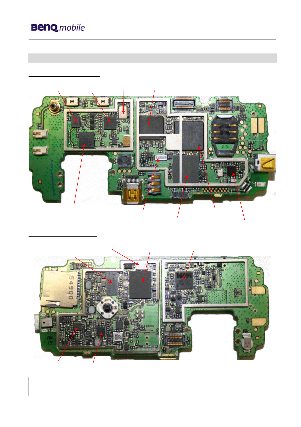
5 PCB Main Board Overview
PCB Main Board Back Side
26 MHz Oscillato
r
IOT
A
A
ntenna Switch Bri
g
ht
P
A
G2 Cal
yp
so
BT Chi
p
Combo Memor
y
32,768 kHz Oscillato
r
PCB Main Board Top Side
MMP
A
udio Codec
48 MHz Oscillato
r
Level Shifter IC
PMIC
Char
g
in
g
IC
Company Confidential
2006©BenQ Mobile

Release 1.0
Technical Documentation
02/2006
TD_Repair_L3_Theory of Operation_S88_R1.0.pdf Page 9 of 54
6 Radio Part Introduction
The radio part is realizes the conversion of the GMSK-HF-signals from the antenna to the
baseband and vice versa.
In the receiving direction, the signals are split in the I- and Q-component and led to the D/A-
converter of the logic part. In the transmission direction, the GMSK-signal is generated in an
Up Conversion Modulation Phase Locked Loop by modulation of the I- and Q-signals which
were generated in the logic part. After that the signals are amplified in the power amplifier.
Transmitter and Receiver are never active at the same time. Simultaneous receiving in the
EGSM900 and GSM1800 band is impossible. Simultaneous transmission in the EGSM900
and GSM1800 band is impossible, too. However the monitoring band (monitoring timeslot)
in the TDMA-frame can be chosen independently of the receiving respectively the
transmitting band (RX- and TX timeslot of the band).
The RF-part is dimensioned for triple band operation (EGSM900, DCS1800, PCS19000).
The RF-circuit consists of the following components:
•Hitachi Bright 6E chip set (HD155165BP) with the following functionality:
oPLL for local oscillator LO1 and LO2 and TxVCO
oIntegrated local oscillators LO1, LO2
oIntegrated TxVCO
oDirect conversion receiver including LNA, DC-mixer, channel filtering and
PGC-amplifier
o26 MHz reference oscillator
•RF 3166 Transmitter power amplifier with integrated power control circuitry
•GSM Quad Band Antenna Switch Module with Dual low-pass filters CXG1180EQ
•Quartz and passive circuitry of the 26MHz VCXO reference oscillator
Company Confidential
2006©BenQ Mobile

Release 1.0
Technical Documentation
02/2006
TD_Repair_L3_Theory of Operation_S88_R1.0.pdf Page 10 of 54
6.1 Block diagrams RF part
RX Part:
TX Part:
Company Confidential
2006©BenQ Mobile

Release 1.0
Technical Documentation
02/2006
TD_Repair_L3_Theory of Operation_S88_R1.0.pdf Page 11 of 54
6.2 BRIGHT VI E chipset (HD 155165BP)
6.2.1 First Local Oscillator
The first local oscillator (LO1) consists of a PLL and VCO inside Bright VI E and an internal
loop filter
6.2.2 RF-PLL
The frequency-step is 400 kHz in DCS1800/PCS1900 mode and 800kHz in
GSM850/EGSM900 mode due to the internal divider by two for DCS1800/PCS1900 and
divider by four for GSM850/EGSM900. To achieve the required settling-time in GPRS
operation, the PLL can operate in fast-lock mode a certain period after programming to
ensure a fast settling. After this the loop filter and current are switched into normal mode to
get the necessary phase noise performance. The PLL is controlled via the tree-wire-bus
(SDI
G2.H11
, SCLK
G2.J14
and SEN
G2.J12
) of Bright VI E.
6.2.3 RF VCO (LO1)
The first local oscillator is needed to generate frequencies which enable the transceiver IC
to demodulate the receiver signal and to perform the channel selection in the TX part. The
full oscillation range is divided into 256 sub-bands. To do so, a control voltage for the LO1 is
used, gained by a comparator. This control voltage is a result of the comparison of the
divided LO1 and the 26MHz reference Signal. The division ratio of the dividers is
programmed by the G2, according to the network channel requirements.
6.2.4 Second local oscillator (640~656MHz)
The second local oscillator (LO2) consists of a PLL and VCO inside Bright (IC201) and an
internal loop filter. Due to the direct conversion receiver architecture, the LO2 is only used
for transmit-operation. The LO2 covers a frequency range of at least 16 MHz (640MHz –
656MHz).
Before the LO2-signal gets to the modulator it is divided by 8. So the resulting TX-IF
frequencies are 80/82 MHz (dependent on the channel and band). The LO2 PLL and power-
up of the VCO is controlled via the tree-wire-bus of Bright (G2 signals SDI
G2.H11
, SCLK
G2.J14
and SEN
G2.J12
). To ensure the frequency stability, the 640MHz VCO signal is
compared by the phase detector of the 2
nd
PLL with the 26 MHz reference signal. The
resulting control signal passes the external loop filter and is used to control the 640/656MHz
VCO.
Company Confidential
2006©BenQ Mobile

Release 1.0
Technical Documentation
02/2006
TD_Repair_L3_Theory of Operation_S88_R1.0.pdf Page 12 of 54
6.2.5 Receiver
The filters are centred to the band frequencies. The symmetrical filter output is matched to
the LNA input of the Bright .The Bright 6E incorporates three RF LNAs for
GSM850/EGSM900, GSM1800 and GSM1900 operation. The LNA/mixer can be switched
in High- and Low-mode to perform an amplification of ~ 20dB. For the “High Gain“ state the
mixers are optimised to conversion gain and noise figure, in the “Low Gain“ state the mixers
are optimised to large-signal behaviour for operation at a high input level. The Bright
performs a direct conversion mixer, which are IQ-demodulators. For the demodulation of the
received GSM signals the LO1 is required. The channel depending LO1 frequencies for
1800MHz/1900MHz bands are divided by 2 and by 4 for 850MHG/900MHz band.
Furthermore the IC includes a programmable gain baseband amplifier PGA (90 dB range,
2dB steps) with automatic DC-offset calibration. LNA and PGA are controlled via G2 (SDI
G2.H11
, SCLK
G2.J14
and SEN
G2.J12
). The channel-filtering is realized inside the chip with
a three stage baseband filter for both IQ chains. The IQ receive signals are fed into the A/D
converters in the IOTA (BIN
IOTA.D10
, BIP
IOTA.D9
BQP
IOTA.C10
, BQN
IOTA.C9
).
6.2.6 Transmitter
Transmitter: Modulator and Up-conversion Loop
The generation of the GMSK-modulated signal in Bright is based on the principle of up
conversion modulation phase locked loop. The incoming IQ-signals from the baseband are
mixed with the divided LO2-signal. The modulator is followed by a lowpass filter (corner
frequency ~80 MHz) which is necessary to attenuate RF harmonics generated by the
modulator. A similar filter is used in the feedback-path of the down conversion mixer.
With help of an offset PLL the IF-signal becomes the modulated signal at the final transmit
frequency. Therefore the GMSK modulated RF-signal at the output of the TX-VCOs is
mixed with the divided LO1-signal to a IF-signal and sent to the phase detector. The I/Q
modulated signal with a centre frequency of the intermediate frequency is send to the phase
detector as well.
The output signal of the phase detector controls the TxVCO and is processed by a loop filter
whose component C619 is external to the Bright. The TxVCO which is realized inside the
Bright chip generates the GSMK modulated frequency.
Company Confidential
2006©BenQ Mobile

Release 1.0
Technical Documentation
02/2006
TD_Repair_L3_Theory of Operation_S88_R1.0.pdf Page 13 of 54
6.2.7 Bright IC Overview
Company Confidential
2006©BenQ Mobile
Release 1.0
Technical Documentation
02/2006
TD_Repair_L3_Theory of Operation_S88_R1.0.pdf Page 14 of 54
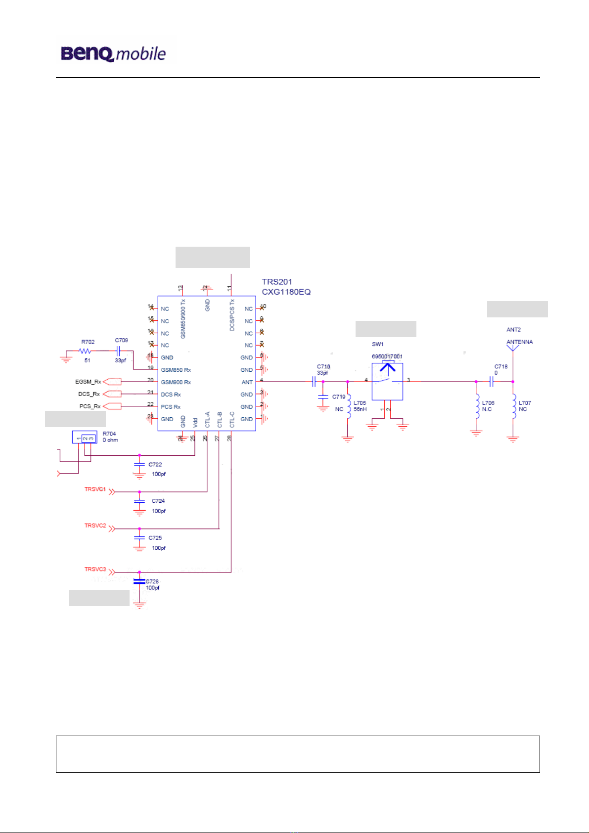
6.3 Antenna switch (electrical/mechanical)
Internal/External <> Receiver/Transmitter
The S88 mobile have two antenna switches.
a) The mechanical antenna switch SW1 for the differentiation between the internal and
external antenna.
b) The electrical antenna switch TRS201, for the differentiation between the receiving
and transmitting signals.
To activate the correct tx pathes of this diplexer, the G2 signals TRSVC1
G2.M14
, TRSVC2
G2.L12
and TRSVC3
G2.L13
are required.
to RX path
In
ternal
External
from PA
from G2
Company Confidential
2006©BenQ Mobile

Release 1.0
Technical Documentation
02/2006
TD_Repair_L3_Theory of Operation_S88_R1.0.pdf Page 15 of 54
6.4 RF Micro Devices transmitter power amplifier RF3166
The RF3166 is a quad-band GSM850, EGSM900, DCS1800, and PCS1900 power amplifier
module that incorporates an indirect closed loop method of power control. The indirect
closed loop is driven directly from the output of the Bright chipset GSMPA
IC201.J5
and
DCSPA
IC201.J4
.
.
Company Confidential
2006©BenQ Mobile

Release 1.0
Technical Documentation
02/2006
TD_Repair_L3_Theory of Operation_S88_R1.0.pdf Page 16 of 54
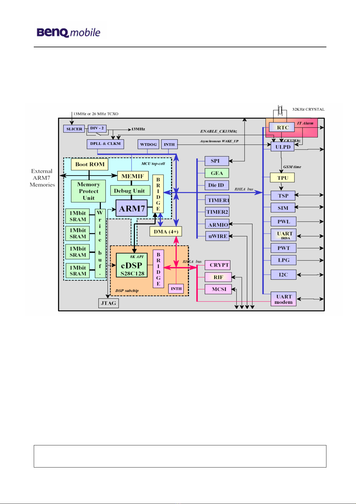
7 Logic / Control Introduction
S88 utilizes TI chipsets (CALYPSO and IOTA) and RENESAS chipset (SHJ2) as base-band
solution. Base-band is composed with three parts: Logic, Analog/Codec and MMP.
CALYPSO is a GSM/GPRS digital base-band logic solution included microprocessor, DSP,
and peripherals. IOTA is a combination of analog/codec solution and power management
which contain base-band codec, voice-band codec, several voltage regulators and SIM level
shifter etc. SHJ2 is a multimedia solution included microprocessor, DSP, internal memory,
and interrupt controller. In addition, S88 integrates with other features such as LED
backlight, OLED display, CMOS DSC module, Micro-SD card, vibration, melody and
charging etc.
7.1 S88 Logic Block Diagram
Company Confidential
2006©BenQ Mobile
Release 1.0
Technical Documentation
02/2006
TD_Repair_L3_Theory of Operation_S88_R1.0.pdf Page 17 of 54
7.2 Calypso - TWL3014
Block diagram
Company Confidential
2006©BenQ Mobile

Release 1.0
Technical Documentation
02/2006
TD_Repair_L3_Theory of Operation_S88_R1.0.pdf Page 18 of 54
7.2.1 Operation theory
CALYPSO (HERCROM400) is a chip implementing the digital base-band processor of a
GSM/GPRS mobile phone. This chip combines a DSP sub-chip (LEAD2 CPU) with its
program and data memories, a Micro-Controller core with emulation facilities (ARM7TDMIE)
and an internal 4M-bit RAM memory, a clock squarer cell, several compiled single-port or 2-
ports RAM and CMOS gates.
Major functions of this chip are as follows:
Real Time Clock (RTC)
The RTC block is an embedded RTC module fed with an external 32.768KHz Crystal. Its
basic functions are:
•Time information (seconds/minutes/hours)
•Calendar information (Day/Month/Year/ Day of the week) up to year 2099
•Alarm function with interrupts (RTCINT is generated to wake up ABB)
•32KHz oscillator frequency gauging
Pulse Width Light (PWL)
This module allows the control of the backlight of LCD and keypad by employing a 4096 bit
random sequence.
MODEM-UART
This UART interface is compatible with the NS 16C750 device which is devoted to the
connection to a MODEM through a standard wired interface. The module integrates two 64
words (9 and 11 bits) receive and transmit FIFOs which trigger levels are programmable. All
modem operations are controllable either via a software interface or using hardware flow
control signals. In Hyperion B1, we implement software flow control by only two signals:
TXD and RXD.
I2C master serial interface (I2C)
The I2C (Philips standard) is a half-duplex serial port using 2 lines (data and clock) for data
transmission with software addressable external devices. In Hyperion B1, we employ I2C
bus to control CLI in Audio Codec.
The I2C signals are defined as follows:
I2C_SCL: programmed to the fast transmission mode (400KHz)
I2C_SDA: the serial bi-directional data of the Audio Codec controller
Company Confidential
2006©BenQ Mobile

Release 1.0
Technical Documentation
02/2006
TD_Repair_L3_Theory of Operation_S88_R1.0.pdf Page 19 of 54
General Purposes I/O (GPIO)
Calypso provides 16 GPIOs configurable in read or write mode by internal registers. In
Hyperion B1, we utilize all of them as follows:
IO0: Let MMP power-on reset; ‘Low active’
IO1: Enable OLED Power; ‘H’ enable, ‘L’ disable
IO2: Control MMP’s MFI mode; ‘H’68-type mode, ‘L’80-type mode
IO3: Camera/Video Mode switch select; ’H’ Camera mode, ’L’ Video mode
IO4: MMP’s MFI INT request; ‘Low active’
IO5: SIM power control
IO6: MMP PMIC mode switch; ’H’ normal mode, ’L’ standby mode
IO7: Reset of external device: For Hyperion B1, Reset for 3 combo memory and OLED
IO8: Indicates whether MMP is in software standby mode
IO9: OLED brightness control; ‘H’ Brighter, ‘L’ Dimmer
IO10:Detection of T-Flash card; ‘H’ No plugged in, ‘L’ plugged in
IO11:OLED brightness control
IO12:OLED brightness control
IO13:INT request for MMP
IO14:SRAM high-byte enable
IO15:SRAM low-byte enable
Serial Port Interface (SPI)
The SPI is a full-duplex serial port configurable from 1 to 32 bits and provides 3 enable
signals programmable either as positive or negative edge or level sensitive. This interface
is working on 13MHz and is used for the GSM/GPRS baseband and voice A/D, D/A with
IOTA
Memory Interface and internal Static RAM
For external memory device (Flash and SRAM), this interface performs read and write
access with adaptation to the memory width. It also provides 6 chip-select signals
corresponding each to an address range of 8 mega bytes. One of these chip-select is
dedicated to the selection of an internal memory. In Hyperion B1, we employ nCS0/nCS1
(nCS0_NROM/nCS1_NROM) for external Flash and nCS2 (nCS2_NSRAM) for external
SRAM. A 4Mbit SRAM is embedded on the die and memory mapped on the chip-select
nCS6 of the memory interface.
SIM Interface
The Subscriber Identity Module interface will be fully compliant with the GSM 11.11 and
ISO/IEC 7816-3 standards. Its external interface is 3 Volts only. 5 Volts adaptation will be
based on external level shifters.
Company Confidential
2006©BenQ Mobile
Release 1.0
Technical Documentation
02/2006
TD_Repair_L3_Theory of Operation_S88_R1.0.pdf Page 20 of 54
Time Serial Port (TSP)
The TPU is a real-time sequencer dedicated to the monitoring of GSM/GPRS baseband
processing. The TSP is a peripheral of the TPU which includes both a serial port (32 bits)
and a parallel interface. The serial port can be programmed by the TPU with a time
accuracy of the quarter of GSM bit. The serial port is uni-directional (transmit only) when
used with IOTA. The serial port provides 4 enable signals programmable either as positive
or negative edge or level sensitive. This serial port is derived from 6.5MHz and used to
control the real time GSM windows for the baseband codec and the windows for ADC
conversion.
TSP Parallel interface (ACT)
The parallel interface allows control 13 external individual outputs and 1 internal signal with
a time accuracy of the quarter of GSM bit. These parallel signals are mainly used to control
the RF activity. In Hyperion B1, we employ 8 of them to control RF activity.
TSPACT0: TR switch power
trol_A
ol_B
rol_C
ection
nable
TSPACT1: TR switch con
TSPACT2: TR switch contr
TSPACT3: TR switch cont
TSPACT5: Band sel
TSPACT6: PA enable
TSPACT8: Crystal e
TSPACT10: Three wires latch enable
Radio Interface (RIF)
The RIF (Radio Interface) Module is a buffered serial port derived from the BSP peripheral
module of the defined for TMS320C5X. The external serial data transmission is supported
by a full-duplex double-buffered serial port interface. The interface is used for transfer of
baseband transmit and receive data and also to access all internal programmation registers
of the device.
Miscellaneous:
Some important Baseband /RF interface signals are defined as follows:
•CLKTCXO: 13MHz VTCXO Clock from RF circuit
•TCXOEN: 13MHz VTCXO Clock Enable signal
Company Confidential
2006©BenQ Mobile
Other manuals for S88
1
Table of contents
Other BenQ mobile Cell Phone manuals

BenQ mobile
BenQ mobile EF51 User manual

BenQ mobile
BenQ mobile EF51 User manual

BenQ mobile
BenQ mobile A38 User manual

BenQ mobile
BenQ mobile M315 Setup guide

BenQ mobile
BenQ mobile S75 User manual

BenQ mobile
BenQ mobile S88 User manual

BenQ mobile
BenQ mobile A38 User manual

BenQ mobile
BenQ mobile S68 User manual

BenQ mobile
BenQ mobile SL75 Setup guide


