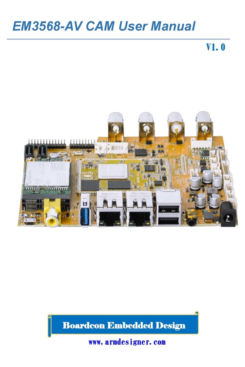
Boardcon Embedded Design EM3566 User manual

EM3566 Hardware Manual
V1.20210730
www.boardcon.com
Boardcon Embedded Design

1
Customize the embedded system based on YourIdea
1. Introduction
1.1. About this Manual
This manual is intended to provide the user with an overview of the board and benefits, complete
features specifications, and set up procedures. It contains important safety information as well.
1.2. Feedback and Update to this Manual
To help our customers make the most of our products, we are continually making additional and
updated resources available on the Boardcon website (www.boardcon.com , www.armdesigner.com).
These include manuals, application notes, programming examples, and updated software and
hardware. Check in periodically to see what’s new!
When we are prioritizing work on these updated resources, feedback from customers is the number
one influence, If you have questions, comments, or concerns about your product or project, please
no hesitate to contact us at support@armdesigner.com.
1.3. Limited Warranty
Boardcon warrants this product to be free of defects in material and workmanship for a period of one
year from date of buy. During this warranty period Boardcon will repair or replace the defective unit
in accordance with the following process:
A copy of the original invoice must be included when returning the defective unit to Boardcon. This
limited warranty does not cover damages resulting from lighting or other power surges, misuse,
abuse, abnormal conditions of operation, or attempts to alter or modify the function of the product.
This warranty is limited to the repair or replacement of the defective unit. In no event shall Boardcon
be liable or responsible for any loss or damages, including but not limited to any lost profits, incidental
or consequential damages, loss of business, or anticipatory profits arising from the use or inability
to use this product.
Repairs make after the expiration of the warranty period are subject to a repair charge and the cost
of return shipping. Please contact Boardcon to arrange for any repair service and to obtain repair
charge information.

2
Customize the embedded system based on YourIdea
Content
1 EM3566 Introduction ......................................................................................................................3
1.1 Summary..............................................................................................................................3
1.2 RK3566 Specifications.........................................................................................................3
1.3 EM3566 Features.................................................................................................................4
1.4 PCB Dimension....................................................................................................................6
1.5 Block Diagram......................................................................................................................7
1.6 CPU module Introduction .....................................................................................................7
2 Peripherals Introduction ...............................................................................................................14
2.1 Power (P1) .........................................................................................................................14
2.2 Audio I/O ............................................................................................................................14
2.3 HDMI OUT (J4) ..................................................................................................................15
2.4 USB OTG (J29)..................................................................................................................16
2.5 USB HOST (P3, J6, J17)....................................................................................................16
2.6 USB3.0/SATA3.0 (J25, J34) ...............................................................................................17
2.7 Ethernet (JP1) ....................................................................................................................18
2.8 eDP/LVDS/MIPI Panel (CON1) ..........................................................................................19
2.9 BT656 (J26) .......................................................................................................................20
2.10 GPIO (CON4)...................................................................................................................21
2.11 ADC (J18).........................................................................................................................21
2.12 MIPI Camera (J30, J31) ...................................................................................................22
2.13 IR (J24) ............................................................................................................................23
2.14 UART (J10, J11, J12) .......................................................................................................23
2.15 RS485 (J32, JP2) .............................................................................................................24
2.16 Button (K3) .......................................................................................................................25
2.17 4G Module (CON2, P4)....................................................................................................25
2.18 Micro SD (J3) ...................................................................................................................26
2.19 WiFi&Bluetooth (U20) ......................................................................................................27
2.20 SSD (CON3) ....................................................................................................................29
2.22 GPS (MU4).......................................................................................................................30
2.23 RTC (BT1)........................................................................................................................31
3 Product Configurations .................................................................................................................32
3.1 Standard Contents .............................................................................................................32
3.2 Optional Parts ....................................................................................................................32

3
Customize the embedded system based on YourIdea
1 EM3566 Introduction
1.1 Summary
The EM3566 is a single-board computer powered by a Rockchip RK3566 processor featuring four
ARM Cortex-A55 CPU cores and Mali-G52-2EE graphics and designed for AIoT applications such
as AI robot, smart POS machine, face recognition terminal, and business display integrated
equipment.
This SBC features 2GB memory (up to 8GB), comes with MIPI/LVDS, HDMI and eDP video out, and
offers Gigabit Ethernet port, as well as M.2 socket which enables expansion with a large hard drive
and plus a miniPCIe, a Nano SIM card socket for 4G cellular connectivity. Display and camera
capabilities with graphics and video hardware acceleration make it suitable for machine vision
applications. And built-in independent NPU, computing power of 0.8 TOPS for AI accelerator extend
the reach of AI solutions. EM3566 supports microphone array input, with high dynamic noise
reduction algorithm, it can accurately recognize human voices even in noisy environments, and
achieve precise voice control of the devices.
1.2 RK3566 Specifications
Specifications
SOC
RockChip RK3566
CPU
Quad-core 64-bit Cortex-A55, 22nm lithography process, frequency up to
1.8GHz
GPU
ARM G52 2EE
Supports OpenGL ES 1.1/2.0/3.2. OpenCL 2.0. Vulkan 1.1
Embedded high-performance 2D acceleration hardware
NPU
0.8Tops@INT8, integrated high-performance AI accelerator RKNN NPU
Supports one-click switching of
Caffe/TensorFlow/TFLite/ONNX/PyTorch/Keras/Darknet
Hardware Features

4
Customize the embedded system based on YourIdea
1.3 EM3566 Features
Specifications
CPU
Rockchip RK3566 quad-core Cortex-A55 @ up to 1.8GHz
Memory
2GB, 4GB, or 8GB LPDDR4 RAM
32Bit, supports all-data-link ECC
Power in
Headphone
USB3.0
Host USB
OTG
HDMI
Ethernet
2x USB2.0
Host
OPT
USB2.0 Host
USB2.0 Host
Camera
Camera
RTC
RS485
LVDS/MIPI/eDPGPIO MEMS
Module
UART2
UART1
WiFi&BT
SIM Card
SD Card
ADC
SATA Power
SATA
SATA/USB3.0
Switch
Recover
Debug
IR
mPCIE
4G&GPS
M.2
NVMe

5
Customize the embedded system based on YourIdea
Storage
8GB / 32GB / 64GB / 128GB eMMC
M.2 PCIe 2.0 socket NVMe SSD (Expand with 2242 NVMe SSD)
MicroSD card slot (Expand with TF card)
SATA3.0 (can switch between SATA and USB 3.0)
Power Supply
12V/3A DC input jack
USB
1x USB OTG 2.0
4x USB Host 2.0 (USB-AF or 4-pin connector)
1x USB 3.0
Connectivity
Gigabit Ethernet RJ45 ports via Realtek RTL8211F-CG controller
2.4G WiFi(802.11b/g/n) with Bluetooth 4.0
mPCIe socket with Nano SIM card port to support 4G&GPS module
Serial
1x Serial port for debug, 3-pin connector
2x UART, 4-pin connectors
1x RS485, 2-pin header or 3-pin connector
Video
HDMI 2.0, 4Kp60
MIPI DSI/LVDS, 1080p60
eDP 1.3, 2560x1600@60Hz
MEMS_Module for Video output
Audio
3.5mm audio I/O jack. ES8388 audio codec
8-channel audio via HDMI
SPDIF out
Camera(optional)
2x Cameras via MIPI CSI (24pin FPC connector)
Keys & Switch
1x Recover Key .1x Switch for switch between SATA and USB 3.0
Other features
RTC with battery connector; IR receiver; GPIO; ADC
Dimension
135mm x 95mm

6
Customize the embedded system based on YourIdea
1.4 PCB Dimension
135mm
95mm

7
Customize the embedded system based on YourIdea
1.5 Block Diagram
1.6 CPU module Introduction
The CPU module CM3566 features 2GB LPDDR4 RAM and 8GB eMMC Flash.
CM3566 specifications
Pin number – 186 pins, 0.9mm pitch
Dimension – 40mm x 47mm
Layer – 8 Layers, complying with EMS/EMI
Power supply – DC 3.3V
Application – smart Device, advertising devices, TV box, POS systems, vehicle control terminals,
AI robot, business display integrated equipment, etc.
4x ARM
Cortex-A55
USB2.0 OTG
USB2.0
OTG PCIe/SATA2 M.2
NVMe
USB3.0/
SATA1
USB3.0/
SATA SDMMC1 Micro SD
CM3566
eDP
UART3
RS485
LPDDR4
up to 8GB iNAND
up to 128GB
Camera1
Debug
UART2 Debug
USB-to-UART
MIPI CSICamera2
UART4
UART5
USB2.0 HOST 2x UART
mPCIe
4G&GPS
40pin header
VOP
HDMIHDMI OUT BT656 14pin header
CIF/GPIO
14pin header
I2S
Codec RTC RTC batteryAudio I/O
UART1/
SDMMC2
USB2.0 HOST
USB HUB WiFi&BT
BL-R8723RD2
4x USB2.0
MIPI/LVDS
option
RGMII MIPI DSI/
LVDS
RJ45 GbE
SIM card
eDP
SARADC ADC
SPDIF
OPT P WM3 _IR IR IN
Power DC/DC

8
Customize the embedded system based on YourIdea
Pin Definition
Pin
Signal
Description or functions
GPIO serial
IO Voltage
1
VCC3V3_SYS
3.3V Main Power input
3.3V
2
VCC3V3_SYS
3.3V Main Power input
3.3V
3
VCC3V3_SYS
3.3V Main Power input
3.3V
4
VCC_RTC
RTC button Cell Power
input
3.0V-1.8V
5
PMIC_32KOUT
RTC clock(32.768khz)
output
3.3V
6
GND
Ground
0V
7
HDMITX_CEC_M0
GPIO4_D1_u
3.3V
8
HDMITX_SDA
Pull up 2.2K inside
GPIO4_D0_u
3.3V
9
HDMITX_SCL
Pull up 2.2K inside
GPIO4_C7_u
3.3V
10
GND
Ground
0V
11
GMAC1_MCLKINOUT
_M0
RGMII reference clock
input(125Mhz)
GPIO3_C0_d
3.3V
12
GND
Ground
0V
13
GMAC1_TXD0_M0
GPIO3_B5_d
3.3V
14
GMAC1_TXD1_M0
GPIO3_B6_d
3.3V
15
GMAC1_TXEN_M0
GPIO3_B7_d
3.3V
16
GMAC1_RXDV_CRS_
M0
GPIO3_B3_d
3.3V
17
GMAC1_RXD1_M0
GPIO3_B2_d
3.3V
18
GMAC1_RXD0_M0
GPIO3_B1_d
3.3V
19
GMAC1_RXD3_M0
GPIO3_A5_d
3.3V
20
GMAC1_RXD2_M0
GPIO3_A4_d
3.3V
21
GMAC1_RXCLK_M0
GPIO3_A7_d
3.3V

9
Customize the embedded system based on YourIdea
Pin
Signal
Description or functions
GPIO serial
IO Voltage
22
GMAC1_TXD2_M0
GPIO3_A2_d
3.3V
23
GMAC1_TXD3_M0
GPIO3_A3_d
3.3V
24
GMAC1_TXCLK_M0
GPIO3_A6_d
3.3V
25
MIPI_DSI_TX0_D3N/L
VDS_TX0_D3N
MIPI DSI or LVDS TXD3N
1.8V
26
MIPI_DSI_TX0_D3P/L
VDS_TX0_D3P
MIPI DSI or LVDS TXD3P
1.8V
27
MIPI_DSI_TX0_D2N/L
VDS_TX0_D2N
MIPI DSI or LVDS TXD2N
1.8V
28
MIPI_DSI_TX0_D2P/L
VDS_TX0_D2P
MIPI DSI or LVDS TXD2P
1.8V
29
MIPI_DSI_TX0_D1N/L
VDS_TX0_D1N
MIPI DSI or LVDS TXD1N
1.8V
30
MIPI_DSI_TX0_D1P/L
VDS_TX0_D1P
MIPI DSI or LVDS TXD1P
1.8V
31
MIPI_DSI_TX0_D0N/L
VDS_TX0_D0N
MIPI DSI or LVDS TXD1N
1.8V
32
MIPI_DSI_TX0_D0P/L
VDS_TX0_D0P
MIPI DSI or LVDS TXD1P
1.8V
33
MIPI_DSI_TX0_CLKN/
LVDS_TX0_CLKN
MIPI DSI or LVDS TXD1N
1.8V
34
MIPI_DSI_TX0_CLKP/
LVDS_TX0_CLKP
MIPI DSI or LVDS TXD1P
1.8V
35
HDMI_TX_HPDIN
HDMI HPD input
3.3V
36
HDMI_TXCLKN
1.8V
37
HDMI_TXCLKP
1.8V
38
HDMI_TX0N
1.8V
39
HDMI_TX0P
1.8V
40
HDMI_TX1N
1.8V
41
HDMI_TX1P
1.8V
42
HDMI_TX2N
1.8V
43
HDMI_TX2P
1.8V
44
MIPI_CSI_RX_CLK1N
MIPI CSI1 CLKN
1.8V
45
MIPI_CSI_RX_CLK1P
MIPI CSI1 CLKP
1.8V
46
MIPI_CSI_RX_D3N
CSI0 RXD3N or CSI1
RXD1N
1.8V
47
MIPI_CSI_RX_D3P
CSI0 RXD3P or CSI1
RXD1P
1.8V
48
MIPI_CSI_RX_D2N
CSI0 RXD2N or CSI1
RXD0N
1.8V
49
MIPI_CSI_RX_D2P
CSI0 RXD2P or CSI1
RXD0P
1.8V

10
Customize the embedded system based on YourIdea
Pin
Signal
Description or functions
GPIO serial
IO Voltage
50
MIPI_CSI_RX_D1P
CSI0 RXD1P
1.8V
51
MIPI_CSI_RX_D1N
CSI0 RXD1N
1.8V
52
MIPI_CSI_RX_D0N
CSI0 RXD0N
1.8V
53
MIPI_CSI_RX_D0P
CSI0 RXD0P
1.8V
54
MIPI_CSI_RX_CLK0N
MIPI CSI0 CLKN
1.8V
55
MIPI_CSI_RX_CLK0P
MIPI CSI0 CLKP
1.8V
56
GND
Ground
0V
57
PWM5
GPIO0_C4_d
3.3V
58
LCD_BL_PWM
PWM4
GPIO0_C3_d
3.3V
59
PWM3_IR
GPIO0_C2_d
3.3V
60
PCIE20_SATA2_RXP
PCIE or SATA2 RXP
1.8V
61
PCIE20_SATA2_RXN
PCIE or SATA2 RXN
1.8V
62
PCIE20_SATA2_TXN
PCIE or SATA2 TXN
1.8V
63
PCIE20_SATA2_TXP
PCIE or SATA2 TXP
1.8V
64
PCIE20_REFCLKP
1.8V
65
PCIE20_REFCLKN
1.8V
66
USB3_HOST1_SSTX
P
USB3.0 or SATA1 TXP
1.8V
67
USB3_HOST1_SSTX
N
USB3.0 or SATA1 TXN
1.8V
68
USB3_HOST1_SSRX
P
USB3.0 or SATA1 RXN
1.8V
69
USB3_HOST1_SSRX
N
USB3.0 or SATA1 RXP
1.8V
70
USB_OTG0_DM
1.8V
71
USB_OTG0_DP
1.8V
72
USB3_HOST1_DP
1.8V
73
USB3_HOST1_DM
1.8V
74
EDP_TX_D2N
1.8V
75
EDP_TX_D2P
1.8V
76
EDP_TX_D1N
1.8V
77
EDP_TX_D1P
1.8V
78
EDP_TX_D0N
1.8V
79
EDP_TX_D0P
1.8V
80
EDP_TX_D3N
1.8V
81
EDP_TX_D3P
1.8V
82
EDP_TX_AUXN
1.8V
83
EDP_TX_AUXP
1.8V
84
SDMMC0_DET_L
GPIO0_A4_u
3.3V
85
SDMMC0_CLK
UART5_TX_M0
GPIO2_A2_d
3.3V
86
GND
Ground
0V
87
SDMMC0_CMD
UART5_RX_M0
GPIO2_A1_u
3.3V

11
Customize the embedded system based on YourIdea
Pin
Signal
Description or functions
GPIO serial
IO Voltage
88
SDMMC0_D3
UART5_RTSn_M0
GPIO2_A0_u
3.3V
89
SDMMC0_D2
UART5_CTSn_M0
GPIO1_D7_u
3.3V
90
SDMMC0_D1
UART6_RX_M1
GPIO1_D6_u
3.3V
91
SDMMC0_D0
UART6_TX_M1
GPIO1_D5_u
3.3V
92
USB_OTG0_ID
3.3V
93
USB_OTG0_VBUSDE
T
USB OTG VBUS input
3.3V
94
UART1_RX_M0
GPIO2_B3_u
1.8V
95
UART1_TX_M0
GPIO2_B4_u
1.8V
96
UART1_RTSn_M0
GPIO2_B5_u
1.8V
97
UART1_CTSn_M0
GPIO2_B6_u
1.8V
98
BT_REG_ON_H
I2S2_SCLK_RX_M0
GPIO2_B7_d
1.8V
99
BT_WAKE_HOST_H
I2S2_LRCLK_RX_M0
GPIO2_C0_d
1.8V
100
HOST_WAKE_BT_H
I2S2_MCLK_M0
GPIO2_C1_d
1.8V
101
WIFI_WAKE_HOST_H
I2C4_SCL_M1
GPIO2_B2_d
1.8V
102
WIFI_REG_ON_H
UART8_RX_M0
GPIO2_C6_d
1.8V
103
I2S2_SCLK_TX_M0
SPI2_MISO_M0
GPIO2_C2_d
1.8V
104
I2S2_LRCK_TX_M0
SPI2_MOSI_M0
GPIO2_C3_d
1.8V
105
I2S2_SDO_M0
SPI2_CS0_M0
GPIO2_C4_d
1.8V
106
I2S2_SDI_M0
UART8_TX_M0
GPIO2_C5_d
1.8V
107
SDMMC1_D3
UART7_TX_M0
GPIO2_A6_u
1.8V
108
SDMMC1_D2
UART7_RX_M0
GPIO2_A5_u
1.8V
109
SDMMC1_D1
UART6_TX_M0
GPIO2_A4_u
1.8V
110
SDMMC1_D0
UART6_RX_M0
GPIO2_A3_u
1.8V
111
SDMMC1_CMD
UART9_RX_M0
GPIO2_A7_u
1.8V
112
SDMMC1_CLK
UART9_TX_M0
GPIO2_B0_d
1.8V
113
GND
Ground
0V
114
SARADC_VIN3
1.8V
115
SARADC_VIN2_HP_H
OOK
1.8V
116
SARADC_VIN0_KEY/
RECOVERY
Pull up 10K inside
1.8V
117
GND
Ground
0V
118
PCIE20_PERSTn_M2
PDM_SDI1_M0
GPIO1_B2_d
3.3V
119
PCIE20_WAKEn_M2
PDM_SDI2_M0
GPIO1_B1_d
3.3V
120
PCIE20_CLKREQn_M
2
PDM_SDI3_M0
GPIO1_B0_d
3.3V
121
UART3_RX_M0
AudioPWM_LOUT_P/I2C3
_SDA_M0
GPIO1_A0_u
3.3V
122
UART3_TX_M0
AudioPWM_LOUT_N/I2C3
_SCL_M0
GPIO1_A1_u
3.3V

12
Customize the embedded system based on YourIdea
Pin
Signal
Description or functions
GPIO serial
IO Voltage
123
UART4_RX_M0
PDM_CLK1_M0/SPDIF_TX
_M0
GPIO1_A4_d
3.3V
124
UART4_TX_M0
AudioPWM_ROUT_P
/PDM_CLK0_M0
GPIO1_A6_d
3.3V
125
I2S1_LRCK_TX_M0_
PMIC
GPIO1_A5_d
3.3V
126
I2S1_SDI0_M0/PDM_
SDI0_M0_PMIC
PDM_SDI0_M0
GPIO1_B3_d
3.3V
127
I2S1_SCLK_TX_M0_
PMIC
UART3_CTSn_M0
GPIO1_A3_d
3.3V
128
I2S1_SDO0_M0_PMI
C
AudioPWM_ROUT_N/UAR
T4_CTSn_M0
GPIO1_A7_d
3.3V
129
I2S1_MCLK_M0_PMI
C
UART3_RTSn_M0
GPIO1_A2_d
3.3V
130
GND
Ground
0V
131
SPI0_CS0_M0
PWM7
GPIO0_C6_d
3.3V
132
SPI0_MISO_M0
PWM6
GPIO0_C5_d
3.3V
133
SPI0_MOSI_M0
I2C2_SDA_M0
GPIO0_B6_u
3.3V
134
SPI0_CLK_M0
I2C2_SCL_M0
GPIO0_B5_u
3.3V
135
SPI3_CS0_M1
I2S3_SDI _M1
GPIO4_C6_d
3.3V
136
SPI3_MISO_M1
I2S3_SDO _M1
GPIO4_C5_d
3.3V
137
SPI3_MOSI_M1
I2S3_SCLK_M1
GPIO4_C3_d
3.3V
138
SPI3_CLK_M1
I2S3_MCLK_M1
GPIO4_C2_d
3.3V
139
LCD_PWREN_H
GPIO0_C7_d
3.3V
140
PWM0_M0
GPIO0_B7_d
3.3V
141
UART5_RX_M1
GPIO3_C3_d
3.3V
142
UART5_TX_M1
GPIO3_C2_d
3.3V
143
UART2DBG_RX
UART2 for Debug
GPIO0_D0_u
3.3V
144
UART2DBG_TX
UART2 for Debug
GPIO0_D1_u
3.3V
145
SPDIF_TX_M2
I2S3_LRCK_M1/EDP_HPD
IN_M0
GPIO4_C4_d
3.3V
146
GPIO0_A6_d
3.3V
147
GPIO0_A3_u
3.3V
148
GPIO0_A0_d
3.3V
149
CAMERAF_RST_L
CAM_CLKOUT1
GPIO4_B0_d
1.8V
150
CAMERAB_RST_L
GPIO4_B1_d
1.8V
151
CIF_8BIT_D7
CIF_D15
GPIO4_A5_d
1.8V
152
CIF_8BIT_D6
CIF_D14
GPIO4_A4_d
1.8V
153
CIF_8BIT_D5
CIF_D13
GPIO4_A3_d
1.8V
154
CIF_8BIT_D4
CIF_D12
GPIO4_A2_d
1.8V
155
CIF_8BIT_D3
CIF_D11
GPIO4_A1_d
1.8V
156
CIF_8BIT_D2
CIF_D10
GPIO4_A0_d
1.8V

13
Customize the embedded system based on YourIdea
Pin
Signal
Description or functions
GPIO serial
IO Voltage
157
CIF_8BIT_D1
CIF_D9
GPIO3_D7_d
1.8V
158
CIF_8BIT_D0
CIF_D8
GPIO3_D6_d
1.8V
159
GND
Ground
0V
160
USB2_HOST2_DM
HOST2_DM
1.8V
161
USB2_HOST2_DP
HOST2_DP
1.8V
162
USB2_HOST3_DP
HOST3_DP
1.8V
163
USB2_HOST3_DM
HOST3_DM
1.8V
164
CIF_8BIT_VSYNC
GPIO4_B7_d
1.8V
165
CIF_8BIT_HREF
GPIO4_B6_d
1.8V
166
CIF_8BIT_CLKIN
GPIO4_C1_d
1.8V
167
GND
Ground
0V
168
CIF_CLKOUT
GPIO4_C0_d
1.8V
169
VOP_BT656_D7_M1
CIF_D7
GPIO3_D5_d
1.8V
170
VOP_BT656_D6_M1
CIF_D6
GPIO3_D4_d
1.8V
171
VOP_BT656_D5_M1
CIF_D5
GPIO3_D3_d
1.8V
172
VOP_BT656_D4_M1
CIF_D4
GPIO3_D2_d
1.8V
173
VOP_BT656_D3_M1
CIF_D3
GPIO3_D1_d
1.8V
174
VOP_BT656_D2_M1
CIF_D2
GPIO3_D0_d
1.8V
175
VOP_BT656_D1_M1
CIF_D1
GPIO3_C7_d
1.8V
176
VOP_BT656_D0_M1
CIF_D0
GPIO3_C6_d
1.8V
177
VOP_BT656_CLK_M1
GPIO4_B4_d
1.8V
178
GPIO4_B5_d_1V8
1.8V
179
I2C4_SDA_M0_1V8
Pull up 2.2K inside
GPIO4_B2_d
1.8V
180
I2C4_SCL_M0_1V8
Pull up 2.2K inside
GPIO4_B3_d
1.8V
181
GND
Ground
0V
182
I2C1_SDA
Pull up 2.2K inside
GPIO0_B4_u
3.3V
183
I2C1_SCL
Pull up 2.2K inside
GPIO0_B3_u
3.3V
184
GPIO0_A5_d
PCIE20_CLKREQn_M0
3.3V
185
GMAC1_MDIO_M0
GPIO3_C5_d
3.3V
186
GMAC1_MDC_M0
GPIO3_C4_d
3.3V
Note:
I2C1 can’t be used for exclusive bus, such as CTP.
RGMII default is 3.3V IO, but can change to 1.8V.

14
Customize the embedded system based on YourIdea
2 Peripherals Introduction
2.1 Power (P1)
The DC JACK is 5.5 x 2.1mm, 3-pin plug Type. Typical 12V/3A DC adapter.
Pin
Signal
Description
Pin
Signal
Description
1
VCC12V_DCIN
Main power supply.
DC 12V power in
2
GND
Ground
3
GND
Ground
2.2 Audio I/O
Headphone (J7, 3.5mm jack)
The EM3566 adopts audio codec ES8388 to provide stereo audio output/input.
Feature
⚫Low power
⚫Integrated ADC and DAC
⚫IIS transfer audio data
⚫Stereo output, support recording
Pin
Signal
Description
Pin
Signal
Description
1
GND
Ground
2
HP_RO
Headphone amplifier
output _Right channel
3
HP_LO
Headphone amplifier
output _Left channel
4
PHE_DET
Headphone Detect
5
MIC2P
Single-end input for microphone
3
1
4
2
5

15
Customize the embedded system based on YourIdea
SPIF-OUT (DJ2)
The Optical Adaptor DLT1120 is used for S/PDIF data output.
Pin
Signal
Description
Pin
Signal
Description
1
SPDIF_TX_M2
SPDIF signal
2
VCC3V3_SYS
3.3V power supply
3
GND
Ground
2.3 HDMI OUT (J4)
EM3566 supports HDMI 2.0 transmitter with HDCP 1.4/2.2, up to 4K@60fps.
⚫HPD input analog comparator
⚫13.5–600MHz input reference clock
⚫Up to 10-bit Deep Color modes
⚫Up to 18Gbps aggregate bandwidth
⚫Up to 1080p at 120Hz and 4kx2k at 60Hz HDTV display resolutions and up to QXGA graphic
display resolutions
⚫3-D video formats
⚫Link controller flexible interface with 30-, 60- or 120-bit SDR data access
Pin
Signal
Description
Pin
Signal
Description
1
HDMI_TX2P
HDMI data 2 pair
2
GND
Ground
3
HDMI_TX2N
4
HDMI_TX1P
HDMI data 1 pair
5
GND
Ground
6
HDMI_TX1N
7
HDMI_TX0P
HDMI data 0 pair
8
GND
Ground
9
HDMI_TX0N
10
HDMI_TXCLKP
HDMI clock pair
11
GND
Ground
12
HDMI_TXCLKN
13
HDMITX_CEC_M0
Consumer
electronics control
14
NC
Not connect
15
HDMI_SCL
HDMI serial clock
16
HDMI_SDA
HDMI serial data
17
GND
Ground
18
HDMI_VCC
5V power supply
19
HDMI_TX_HPDIN
Hot Plug Detect
1
2
3
1
19

16
Customize the embedded system based on YourIdea
2.4 USB OTG (J29)
EM3566 OTG is a Micro USB2.0 port, it is used to download image and ADB transfer file.
Feature
⚫Compatible with USB OTG2.0 specification
⚫Supports USB 2.0 High Speed (480Mbps), Full Speed (12Mbps) and Low Speed (1.5Mbps)
operation in host mode
⚫Supports USB 2.0 High Speed (480 Mbps) and Full Speed (12 Mbps) operation in peripheral
mode.
⚫Hardware support for OTG signaling, session request protocol, and host negotiation protocol.
Pin
Signal
Description
Pin
Signal
Description
1
VCC_OTG
USB OTG Power
2
USB_OTG0DM
USB OTG0 data -
3
USB_OTG0DP
USB OTG0 data+
4
USB_OTG0ID
USB OTG0 ID
indicator
5
GND
Ground
2.5 USB HOST (P3, J6, J17)
EM3566 provides 4x USB2.0 - one dual-USB (P3) and two 4-pin connector (J6, J17).
The 4-ch USB HOST interfaces are extended by GL850G which is a fully compliant with the USB
2.0 hub specification and is designed to work with USB host as a high-speed hub. It is used to
connect USB mouse, U disk, USB camera, and other USB devices. Support hot-plug.
Feature
⚫Supports high-speed (480Mbps), full-speed (12Mbps) and low-speed (1.5Mbps) mode
⚫Supports automatic switching between bus- and self-powered modes
⚫Provides 16 host mode channels
⚫Support periodic out channel in host mode
1
5
1
5
8
4
2 1
3
4

17
Customize the embedded system based on YourIdea
P3 (dual-USB)
Pin
Signal
Description
Pin
Signal
Description
1
VCC_USB
USB Power. DC 5V
2
USB_DM1
USB data-
3
USB_DP1
USB Data+
4
GND
Ground
5
VCC_USB
USB Power. DC 5V
6
USB_DM2
USB data-
7
USB_DP2
USB Data+
8
GND
Ground
J6 / J17 (4-pin connector)
Pin
Signal
Description
Pin
Signal
Description
1
VDD5V0_HOST
2
5V power supply
2
USB_DM4(J6)/
USB_DM3(J17)
USB data-
3
USB_DP4(J6)/
USB_DP3(J17)
USB Data+
4
GND
Ground
2.6 USB3.0/SATA3.0 (J25, J34)
The USB3.0 and SATA3.0 share the same USB signal. The SW1 is a DIP Switch for the selection of
USB3.0 or SATA.
SW1
Mode
1
2
USB3.0
OFF
OFF
SATA
ON
ON
USB3.0(J25)
Pin
Signal
Description
Pin
Signal
Description
1
VCC5V0_HOST1
USB Power. DC 5V
2
USB3_DM
USB data-
3
USB3_DP
USB Data+
4
GND
Ground
5
USB3_SSRXN
USB SSRX Data-
6
USB3_SSRXP
USB SSRX Data+
7
GND
Ground
8
USB3_SSTXN
USB SSTX Data-
9
USB3_SSTXP
USB SSTX Data+
= ON
ON
12
ON
12
1357
24689

18
Customize the embedded system based on YourIdea
EM3566 on-board 7-pin SATA Interface. It requires 5V power supply.
SATA(J34)
Pin
Signal
Description
Pin
Signal
Description
1
GND
Ground
2
USB3_SSTXP
USB SSTX Data+
3
USB3_SSTXN
USB SSTX Data-
4
GND
Ground
5
USB3_SSRXN
USB SSRX Data-
6
USB3_SSRXP
USB SSRX Data+
7
GND
Ground
SATA_Power (J33)
Pin
Signal
Description
Pin
Signal
Description
1
GND
Ground
2
VCC5V0_HOST1
SATA power. DC 5V
2.7 Ethernet (JP1)
EM3566 adopts RTL8211F as the Ethernet chip. RJ45 connector.
Feature
⚫Supports 10/100/1000-Mbps data transfer rates with the MII/RGMII interfaces
⚫Supports both full-duplex and half-duplex operation
⚫Implements the full 802.3 specification
Pin
Signal
Description
Pin
Signal
Description
1
DA+
Bi-directional
transmit/receive pair A
2
DA-
Bi-directional
transmit/receive pair A
3
DB+
Bi-directional
transmit/receive pair B
4
DC+
Bi-directional
transmit/receive pair C
1
7
2 1
1
2
7
8
13
12

19
Customize the embedded system based on YourIdea
Pin
Signal
Description
Pin
Signal
Description
5
DC-
Bi-directional
transmit/receive pair C
6
DB-
Bi-directional
transmit/receive pair B
7
DD+
Bi-directional
transmit/receive pair D
8
DD-
Bi-directional
transmit/receive pair D
9
GND
Ground
10
GND
Ground
11
LED2/CFG_L
DO1
LED2
12
GND
Ground
13
LED1/CFG_L
DO0
LED1
14
GND
Ground
2.8 eDP/LVDS/MIPI Panel (CON1)
EM3566 supports 10.1-inch HD capacitive LCD, up to 1280 x 800 resolution.
Pin
Signal
Description
Pin
Signal
Description
1
VDD5V
5V power supply
2
VDD5V
5V power supply
3
GND
Ground
4
GND
Ground
5
VCC3V3_LCD
3.3V power supply
6
VCC3V3_LCD
3.3V power supply
7
GND
Ground
8
GND
Ground
9
I2C2_SCL_TP
TP I2C serial clock
line
10
I2C2_SDA_TP
TP I2C data line
11
TOUCH_RST
Touch screen reset
12
TOUCH_INT
Touch screen
Interrupt
13
LCD_PWREN_H
LCD Power enable
high
14
LCD_BL_PWM
LCD Backlight PWM
output
15
GND
Ground
16
GND
GND
17
EDP_TX_AUXP
eDP CH-AUX
positive differential
output
18
EDP_TX_AUX
P
eDP CH-AUX
negative differential
output
19
GND
Ground
20
GND
Ground
GND
Power supply
LVDS
SPI
I2C
eDP
LCD
MIPI DSI
Touch
1 3 57 9 11 13 15 17 19 21 23 25
2 4 6 8 10 12 14 16 18 20 22 24 26
21 23 25 27 29 33 35 37 39
28 30
31
32 34 36 38 40
Table of contents
Other Boardcon Embedded Design Motherboard manuals
