Boser HS-2604 User manual

HS-2604
EDEN Embedded Engine Board
•Half Size•All-in-One•CRT/Panel•133MHz FSB•
•ATA/33/66/100•Three LAN•RS-232/422/485•
•4COM•PC/104•IrDA•USB•DOC•
•WDT•H/W Monitor•Single +5V•
•Industrial Embedded Single Board computer•

Copyright Disclaimers
The accuracy of contents in this manual has passed thorough checking and review before
publishing. BOSER Technology Co., Ltd., the manufacturer and publisher, is not liable for
any infringements of patents or other rights resulting from its use. The manufacturer will
not be responsible for any direct, indirect, special, incidental or consequential
damages arising from the use of this product or documentation, even if advised of
the possibility of such damage(s).
This manual is copyrighted and BOSER Technology Co., Ltd. reserves all
documentation rights. Unauthorized reproduction, transmission, translation, and
storage of any form and means (i.e., electronic, mechanical, photocopying, recording)
of this document, in whole or partly, is prohibited, unless granted permission by BOSER
Technology Co., Ltd.
BOSER Technology Co., Ltd. reserves the right to change or improve the contents of
this document without due notice. BOSER Technology Co., Ltd. assumes no
responsibility for any errors or omissions that may appear in this manual, nor does
it make any commitment to update the information contained herein.
T
T
Tr
r
ra
a
ad
d
de
e
em
m
ma
a
ar
r
rk
k
ks
s
s
BOSER is a registered trademark of BOSER Technology Co., Ltd.
ISB is a registered trademark of BOSER Technology Co., Ltd.
VIA is a registered trademark of VIA Technologies, Inc.
AMI is a registered trademark of AMI Software, Inc.
All other trademarks, products and or product names mentioned herein are
mentioned for identification purposes only, and may be trademarks and/or
registered trademarks of their respective companies or owners.
© Copyright 2003 BOSER Technology Co., Ltd.
All Rights Reserved.
Edition 1.1, June 05, 2003

Table of Contents
Chapter 1 General Description ..................................1
1.1 Major Features....................................................................... 2
1.2 Specifications ........................................................................ 3
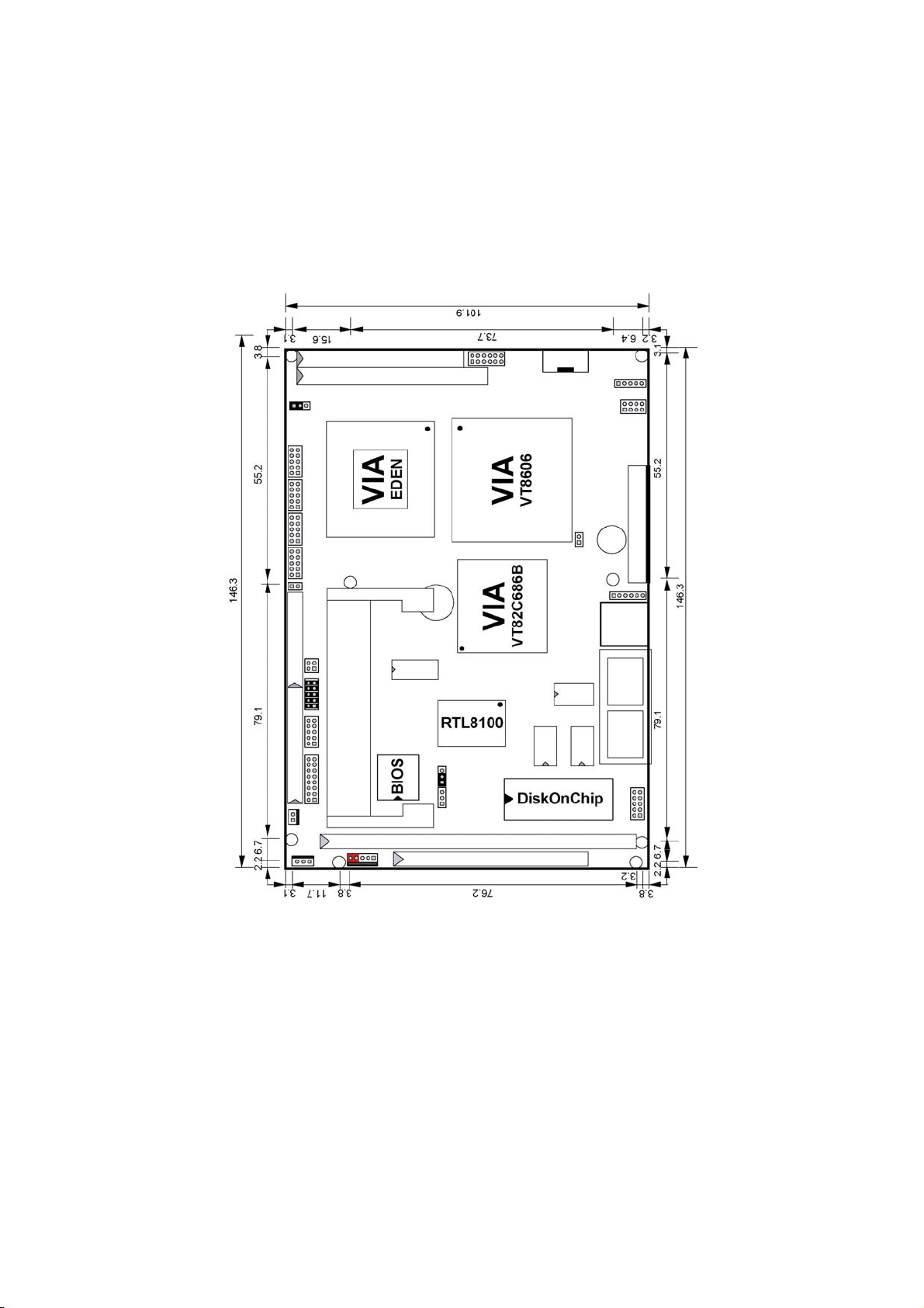
1.3 Board Dimensions................................................................. 4
Chapter 2 Unpacking ..................................................5
2.1 Opening the Delivery Package............................................. 5
2.2 Inspection............................................................................... 5
Chapter 3 Hardware Installation ..............................7
3.1 Before Installation ................................................................. 7
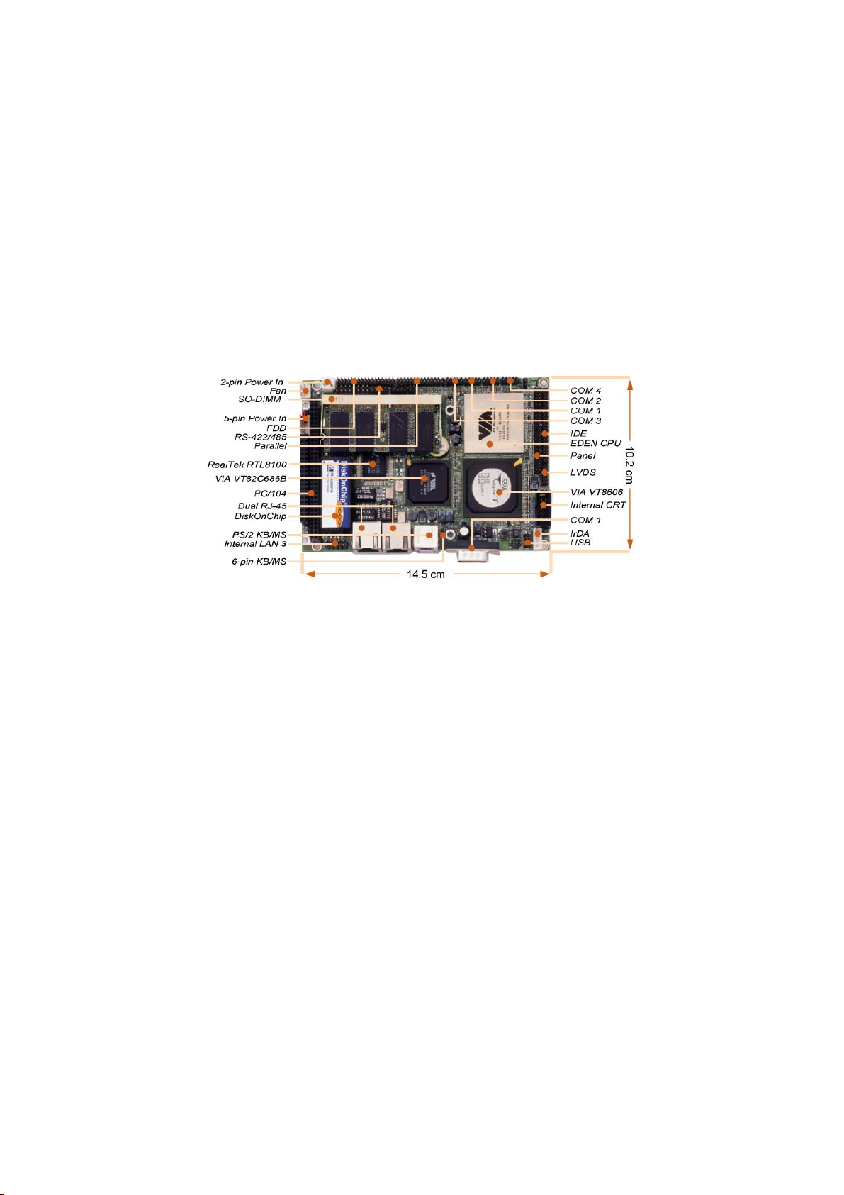
3.2 Board Layout ......................................................................... 8
3.3 Jumper List ............................................................................ 9
3.4 Connector List ....................................................................... 9
3.5 Configuring the CPU ........................................................... 10
3.6 System Memory ................................................................... 10
3.7 DiskOnChipAddress Setting .......................................... 10
3.8 VGA Controller .................................................................... 12
3.9 PCI E-IDE Drive Connector................................................. 14
3.10 Floppy Disk Drive Connector ............................................. 15
3.11 Serial Port Connectors ....................................................... 16
3.12 Parallel Connector............................................................... 18
3.13 Ethernet Connector............................................................. 20
3.14 IrDA Connector.................................................................... 21
3.15 USB Connector.................................................................... 21
3.16 CMOS Data Clear................................................................. 21
3.17 Power and Fan Connectors................................................ 22
3.18 Keyboard/Mouse Connectors ............................................ 22
3.19 System Front Panel Connectors........................................ 23
3.20 Watchdog Timer .................................................................. 24
3.21 Mini PCI Connector ............................................................. 26
3.22 PC/104 Connectors ............................................................. 28
Chapter 4 AMI BIOS Setup .....................................30
4.1 Starting Setup...................................................................... 30
4.2 Using Setup.......................................................................... 31
4.3 Main Menu ............................................................................ 32
4.4 Standard CMOS Setup ........................................................ 33
4.5 Advanced CMOS Setup ...................................................... 34

4.6 Advanced Chipset Setup.................................................... 35
4.7 Power Management Setup ................................................. 36
4.8 PCI / Plug and Play Setup................................................... 37
4.9 Peripheral Setup.................................................................. 38
4.10 Hardware Monitor Setup..................................................... 39
4.11 Auto-Detect Hard Disks ...................................................... 39
4.12 Change Supervisor/User Password .................................. 40
4.13 Auto Configuration with Optimal Settings ....................... 41
4.14 Auto Configuration with Fail Safe Settings...................... 42
4.15 Save Settings and Exit........................................................ 43
4.16 Exit Without Saving............................................................. 44
Chapter 5 Software Utilities..................................... 46
5.1 IDE Driver Installation ......................................................... 46
5.2 VGA Driver Installation ....................................................... 51
5.3 LAN Driver Installation........................................................ 57

Safety Instructions
Integrated circuits on computer boards are sensitive to static electricity. To
avoid damaging chips from electrostatic discharge, observe the following
precautions:
Do not remove boards or integrated circuits from their anti-static packaging
until you are ready to install them.
Before handling a board or integrated circuit, touch an unpainted portion of
the system unit chassis for a few seconds. This helps to discharge any static
electricity on your body.
Wear a wrist-grounding strap, available from most electronic component
stores, when handling boards and components. Fasten the ALLIGATOR clip
of the strap to the end of the shielded wire lead from a grounded object.
Please wear and connect the strap before handle the HS-2604 to ensure
harmlessly discharge any static electricity through the strap.
Please use an anti-static pad when putting down any components or parts or
tools outside the computer. You may also use an anti-static bag instead of
the pad. Please inquire from your local supplier for additional assistance in
finding the necessary anti-static gadgets.
NOTE: DO NOT TOUCH THE BOARD OR ANY OTHER SENSITIVE
COMPONENTS WITHOUT ALL NECESSARY ANTI-STATIC
PROTECTION.


1
Chapter 1
General Description
The HS-2604 is a 100/133MHz FSB VIA VT8606 chipset-based board
designed for Mini PCI Local Bus VIA C3 EDEN 400/667MHz
Embedded CPU. These features combine and make the HS-2604 an
ideal all-in-one industrial single board computer. Additional features
include an enhanced I/O with CRT/Panel, three LAN, and 4COM ports
interfaces.
Its onboard ATA/33/66/100 to IDE drive interface architecture allows
the HS-2604 to support data transfers of 33, 66 or 100MB/sec. to one
IDE drive connection. Designed with the VIA VT8606 core logic
chipset, the board supports VIA C3 EDEN 400/667MHz Embedded
CPU. The VIA VT8606 integrated S3 3D supporting CRT/Panel
displays up to 1920 x 1440.
System memory is also sufficient with the one SO-DIMM socket that
can support up to 256MB.
Additional onboard connectors include an advanced USB and IrDA
ports providing faster data transmission, a DOS-compatible
DiskOnChipsocket with a maximum capacity of 288MB. And two
external RJ-45 connectors and one 10-pin header for 10/100 Based
Ethernet use.

2
To ensure the reliability in an unmanned or standalone system, the
Watchdog Timer (WDT) onboard HS-2604 is designed with pure
hardware that does not need the arithmetical functions of a real-time
clock chip. If any program causes unexpected halts to the system, the
onboard Watchdog Timer (WDT) will automatically reset the CPU or
generate an interrupt to resolve such condition.
1.1 Major Features
The HS-2604 comes with the following features:
VIA C3 EDEN 400/667MHz Embedded CPU
VIA VT8606/VT82C686B system chipset
Supports 100/133MHz FSB
One SO-DIMM socket with a max. capacity of 256MB
SMC 37C669, VIA VT82C686B super I/O chipset
Fast PCI ATA/33/66/100 IDE controller
Three RS-232 and one RS-232/422/485 serial ports
PC/104 Bus connector
VIA VT8606 CRT/Panel display controller
Three RealTek RTL8100 10/100 Based LAN
DiskOnChipsocket supporting memory size of up to 288MB
Two USB connectors
Supports Hardware Monitor function
Supports Single +5V power in

3
1.2 Specifications
CPU: VIA C3 EDEN 400/667MHz embedded CPU
Bus Interface: Mini PCI Local Bus
Memory: One SO-DIMM socket supporting up to 256MB
Chipset: VIA VT8606/VT82C686B
I/O Chipset: SMC 37C669, VIA VT82C686B
VGA: VIA VT8606 integrated S3 3D supporting CRT/Panel displays up
to 1920 x 1440
IDE: Two IDE disk drives supporting ATA/33/66/100 and with transfer
rates of up to 33/66/100MB/sec.
FDD: Supports up to two floppy disk drives
Parallel: One enhanced bi-directional parallel port supporting
SPP/ECP/EPP
LAN: Three RealTek RTL8100 10/100 Based LAN
Serial Port: 16C550 UART-compatible RS-232/422/485 x 1 and RS-232
x 3 serial ports with 16-byte FIFO
PC/104: PC/104 connector for 16-bit ISA Bus
IrDA: One IrDA TX/RX header
USB: Two USB connectors
Keyboard/Mouse: PS/2 6-pin Mini DIN or 6-pin connector
DiskOnChip:DiskOnChipsocket supporting memory sizes of up to
288MB
BIOS: AMI PnP Flash BIOS
Watchdog Timer: Sets 1, 2, 10, 20, 110, 220 seconds, activity trigger
with Reset or NMI
CMOS: Battery backup
Power: Single +5V/3.2A power in
Operating Temperature: -20 ~ +60°C (EDEN 400MHz)
Hardware Monitor: VIA VT82C686B
Board Size: 14.5 x 10.2 cm

4
1.3 Board Dimensions

5
Chapter 2
Unpacking
2.1 Opening the Delivery Package
The HS-2604 is packed in an anti-static bag. The board has
components that are easily damaged by static electricity. Do not
remove the anti-static wrapping until proper precautions have been
taken. Safety Instructions in front of this manual describe anti-static
precautions and procedures.
2.2 Inspection
After unpacking the board, place it on a raised surface and carefully
inspect the board for any damage that might have occurred during
shipment. Ground the board and exercise extreme care to prevent
damage to the board from static electricity.
Integrated circuits will sometimes come out of their sockets during
shipment. Examine all integrated circuits, particularly the BIOS,
processor, memory modules, ROM-Disk, and keyboard controller chip
to ensure that they are firmly seated. The HS-2604 delivery package
contains the following items:
HS-2604 Board x 1
Utility CD Disk x 1
IDE flat cable x 1
FDD flat cable x 1
Printer cable x 1
10-pin VGA cable x 1
One PS/2 KB/MS Transfer cable x 1
One Ethernet cable x 1
One RS-232 COM Port cable x 4
8-pin USB split type cable x 1
2-pin Power cable x 1
Jumper Bag x 1
User’s Manual

6
It is recommended that you keep all the parts of the delivery package
intact and store them in a safe/dry place for any unforeseen event
requiring the return shipment of the product. In case you discover any
missing and/or damaged items from the list of items, please contact
your dealer immediately.

7
Chapter 3
Hardware Installation
This chapter provides the information on how to install the hardware
using the HS-2604. This chapter also contains information related to
jumper settings of switch, watchdog timer, and the DiskOnChip
address selection etc.
3.1 Before Installation
After confirming your package contents, you are now ready to install
your hardware. The following are important reminders and steps to
take before you begin with your installation process.
1. Make sure that all jumper settings match their default settings
and CMOS setup correctly. Refer to the sections on this chapter
for the default settings of each jumper.
2. Go through the connections of all external devices and make
sure that they are installed properly and configured correctly
within the CMOS setup. Refer to the sections on this chapter
for the detailed information on the connectors.
3. Keep the manual and diskette in good condition for future
reference and use.

8
3.2 Board Layout

9
3.3 Jumper List
Jumper
Default Setting Setting Page
JP1 WDT Active Type Setting: Disabled Open 23
JP2 Clear CMOS: Normal Operation Short 1-2 20
JP4(1-4) DOC Address Select: D000 Short 1-2, 3-4 10
JP4(5-10) WDT Timer Select: 1sec. Short 5-6, 7-8,
9-10 23
JP5 RS-422/485 Receiver
Enabled/Disabled Select: Disabled Open 16
JP6 COM2 Use RS-232 or RS-422/485:
RS-232 Open 16
JP7 Panel Voltage: +3.3V Short 1-2 12
3.4 Connector List
Connector
Definition Page
CN1 5-pin ATX Power In Connector 21
CN2 PC/104 40-pin Connector 27
CN3 PC/104 64-pin Connector 27
CN4 2-pin Power In Connector 21
CN6 Floppy Connector 15
CN7 RS-422/485 Connector (5x2 header) 16
CN8 Dual RJ-45 Connector 19
CN9 Parallel Connector 18
CN10 PS/2 6-pin Mini DIN KB/MS Connector 21
CN11 6-pin KB/MS Connector 21
CN12 COM 3 Connector (5x2 header) 16
CN13 COM 1 Connector (DB9) 16
CN14 COM 1 Connector (5x2 header) 16
CN15 COM 2 Connector (5x2 header) 16
CN16 COM 4 Connector (5x2 header) 16
CN17 USB Connector 20
CN19 IrDA Connector 20
CN20 50-pin Panel Connector 12
CN21 CRT Connector (5x2 header) 12
CN22 LVDS Connector 12
CN23 IDE Connector 14
CN24 LAN Connector (5x2 header) 19
DM1 SO-DIMM Socket 10
. . . More on next page . . .

10
Connector Definition Page
FN1 Fan Connector 21
JP3 Front Panel Connector 22
PC1 Mini PCI Connector 25
U1 DiskOnChipTM Socket 10
3.5 Configuring the CPU
The HS-2604 embedded with a VIA C3 EDEN 400/667MHz CPU. User
don’t need to adjust the frequently and check speed of VIA C3 EDEN
CPU.
3.6 System Memory
The HS-2604 provides one SO-DIMM socket at locations DM1. The
maximum capacity of the onboard memory is 256MB.
3.7 DiskOnChipAddress Setting
The DiskOnChipfunction allows the system to boot or operate
without a FDD or a HDD. DiskOnChipmodules may be formatted as
drive C or A. With DiskOnChip, user may also execute DOS
commands such as FORMAT, SYS, COPY, XCOPY, DISCOPY and
DISKCOMP etc.
The U1 location onboard the HS-2604 is the DiskOnChipmodule
socket. Jumper JP4(1-4) assigns the starting memory address of the
installed module. If you have another memory device that has a similar
memory capacity with that of the DOC in your system, please set both
at different memory address mapping to avoid the mapping area
conflicts. Failing to do so will not make the HS-2604 and the additional
memory device function properly.
JP4(1-4): DiskOnChipAddress Select
Address PINS 1-2 PINS 3-4
D000 Short Short
D800 Open Short
E000 Short Open

11
3.7.1 Installing DiskOnChipModules
When installing a DiskOnChipmodule onto your board, please take
note of the following:
1. Orient yourself properly with the location of the DiskOnChip
socket. Try to locate the pin 1 location on your socket. Pin
numbers are usually printed on either the component side or the
solder side of your board.
2. Locate the Pin 1 location on your DiskOnChipmodule. More
often than not, Pin 1 can be found on the lower right corner of
the chip. Please refer to the diagram for the exact location.
3. Once you have figured out where the pin 1 locations are on both
chip and socket, align the module’s pins on an upright angle
against the socket. Using both thumbs, gently press the module
into the socket until all the pins are secured to their
designations.
Pin 1
Location
DiskOnChip
4. The installation is now complete and your module is now ready
for use.
NOTE: If you encounter difficulty installing your DiskOnChip
module,
please consult a qualified technician or engineer to perform the
installation.
3.7.2 Removing DiskOnChipModules
When removing a DiskOnChipmodule from its socket, please take
note of the following:
1. Loosen the contact of the module from its socket using a
screwdriver.

12
2. Insert the screwdriver’s flat head into a gap on either end of the
socket. Do not insert the screwdriver head on either side where
the pins are located. Doing so might damage the pins in the
process.
3. Slowly lift the screwdriver handle upwards. This will disengage
the module from its socket.
NOTE: If you encounter difficulty removing your DiskOnChip
module,
please consult a qualified technician or engineer to remove it for
you.
3.8 VGA Controller
The HS-2604 provides three connection methods of a VGA device.
CN21 offers a single standard CRT connector (5x2 header) while
CN20 is the 50-pin panel connector and CN22 is the LVDS interface
connector onboard reserved for flat panel installation.
CN21: CRT Connector (5x2 header)
PIN
Description
PIN Description
1 Red 2 GND
3 Green 4 GND
5 Blue 6 GND
7 HSYNC 8 SDA
9 VSYNC 10 SCL
2
4
6
8
10
1
3
5
7
9
GND
GND
GND
SCL
SDA
Red
Green
Blue
VSYNC
HSYNC
CN22: LVDS Interface Connector
PIN
Description
PIN
Description
1 VCC3 2 VCC3
3 Y0 4 Y1
5 Y2 6 Y3
7 Y4 8 Y5
9 Y6 10 Y7
11 GND 12 GND
12
1211
VCC3
Y0
Y2
Y4
Y6
GND
VCC3
Y1
Y3
Y5
Y7
GND
NOTE: LVDS cable should be produced very carefully. Y1 & Y2 have to be
fabricated in twister pair (Y2 & Y3, Y4 & Y5, Y6 & Y7 and so on)
otherwise the signal won’t be stable. Please set the proper voltage
of your panel using JP7 before proceeding on installing it.

13
CN20: 50-pin Panel Connector
PIN.
Description
PIN
Description
1 +12V 2 +12V
3 GND 4 GND
5 3.3V / 5V Note 6 ENAVDD
7 ENAVEE 8 GND
9 PD0 10 PD1
11 PD2 12 PD3
13 PD4 14 PD5
15 PD6 16 PD7
17 PD8 18 PD9
19 PD10 20 PD11
21 PD12 22 PD13
23 PD14 24 PD15
25 PD16 26 PD17
27 PD18 28 PD19
29 PD20 30 PD21
31 PD22 32 PD23
33 PD24 34 PD25
35 SHFCLK 36 FLM
37 DE 38 LP
39 GND 40 ENABKL
41 P26 42 P27
43 P28 44 P29
45 P30 46 P31
47 P32 48 P33
49 P34 50 P35
12
5049
+12V
GND
3.3V/5V
ENAVEE
PD0
PD2
PD4
PD6
PD8
PD10
PD12
PD14
PD16
PD18
PD20
+12V
GND
ENAVDD
GND
PD1
PD3
PD5
PD7
PD9
PD11
PD13
PD15
PD17
PD19
PD21
PD22
PD24
SHFCLK
DE
GND
P26
P28
P30
P32
P34
PD23
PD25
FLM
LP
ENABKL
P27
P29
P31
P33
P35
NOTE: Please set the proper voltage of your panel using JP7 before
proceeding on installing it.
The HS-2604 has an onboard jumper that selects the working voltage
of the flat panel connected to the system. Jumper JP7 offers two
voltage settings for the user.
JP7: Panel Voltage Select
Options Settings
3.3 V Short 1-2
5 V Short 2-3
+3.3V
GND
VCC
13

14
3.9 PCI E-IDE Drive Connector
CN23 is a standard 44-pin 2.0mm pitch connector daisy-chain driver
connector serves the PCI E-IDE drive provisions onboard the HS-2604.
A maximum of two ATA/33/66/100 IDE drives can connect to the
HS-2604 via CN23.
CN23: IDE Connector
PIN Description PIN Description
1 Reset 2 GND
3 DATA 7 4 DATA 8
5 DATA 6 6 DATA 9
7 DATA 5 8 DATA 10
9 DATA 4 10 DATA 11
11 DATA 3 12 DATA 12
13 DATA 2 14 DATA 13
15 DATA 1 16 DATA 14
17 DATA 0 18 DATA 15
19 GND 20 N/C
21 PDREQ 22 GND
23 IOW# 24 GND
25 IOR# 26 GND
27 PIORDY 28 PR1PD1-
29 RPDACK- 30 GND
31 Interrupt 32 N/C
33 RPDA1- 34 PATA66
35 RPDA0- 36 RPDA2-
37 RPCS1- 38 RPCS3-
39 HDD Active LED 40 GND
41 VCC 42 VCC
43 GND 44 N/C
-IDERST
PDD7
PDD6
PDD5
PDD4
PDD0
GND
PDDREQ
-PDIOW
-PDIOR
PIORDY
-PDDACK
IRQ14
PDA1
PDD3
PDD2
PDD1
PDA0
-PDCS1
HDD ACTIVE
GND
PDD8
PDD9
PDD10
PDD11
PDD15
N/C
GND
’
GND
GND
GND
GND
N/C
PD33
PDD12
PDD13
PDD14
PDA2
-PDCS3
GND
1
244
43
VCC
GND
VCC
N/C
Table of contents
Other Boser Motherboard manuals