Caen ELS FLUCS CT PCB Series User manual

<
DC Current Transducers
CT PCB Series
User’s Manual
All Rights Reserved
© CAEN ELS s.r.l.
Rev. 1.11 –November 2022
PRECISION CURRENT TRANSDUCERS

2
CAEN ELS s.r.l.
Via Vetraia, 11
55049 Viareggio (LU) –Italy
Mail: [email protected]
Web: www.caenels.com

CT PCB Series User’s Manual
3
Table Of Contents
1. INTRODUCTION................................................................................................8
1.1 CT PCB SERIES OVERVIEW............................................................................8
1.2 CT PCB MODELS AND VERSIONS.................................................................10
2. INSTALLATION AND OPERATION............................................................11
2.1 CONNECTIONS...............................................................................................11
2.2 RECOMMENDED PCB FOOTPRINT .................................................................12
2.3 PCB LAYOUT GUIDELINES ...........................................................................14
2.4 SECONDARY-SIDE SIGNALS...........................................................................14
2.4.1 Power Supply...........................................................................................15
2.4.2 Secondary Current...................................................................................15
2.4.3 Voltage Output (“V” versions only) ........................................................15
2.4.4 OK Signal.................................................................................................16
3. TECHNICAL SPECIFICATIONS ..................................................................18
3.1 EQUIVALENT INPUT NOISE............................................................................19
3.2 EXTERNAL SHUNT RESISTOR ........................................................................20
3.3 ISOLATION DATA ..........................................................................................21
4. MECHANICAL DIMENSIONS.......................................................................22

CT PCB Series User’s Manual
4
Revision
Date
Comment
0.1
March 14th 2013
Document created
1.0
April 4th 2013
First official release
1.1
June 17th 2013
Additional information added
1.2
July 12th 2013
Mechanical dimensions updated
1.3
January 6th 2014
Noise data added and OK+ and OK- changed
pinout
1.4
April 2nd 2014
CT-52 version added
1.5
April 7th 2014
External shunt resistor added
1.6
November 3rd 2014
Manual graphics changed
1.7
March 11th 2015
Offset specification updated
1.8
July 11th 2016
Added data to technical specifications
1.9
March 12th 2018
Added information on GND connection
1.10
June 16th 2020
Added WCT13XLPAAAA model
1.11
November 23rd 2022
Added UKCA compliance logo. Fixed spaces in
Flucs logo along the whole document.

CT PCB Series User’s Manual
5
Safety information - Warnings
CAEN ELS will repair or replace any product within the guarantee period if the
Guarantor declares that the product is defective due to workmanship or materials and
has not been caused by mishandling, negligence on behalf of the User, accident or any
abnormal conditions or operations.
Please read carefully the manual before operating any part of the instrument
WARNING
Do NOT open the boxes
CAEN ELS d.o.o. declines all responsibility for damages or injuries caused
by an improper use of the Modules due to negligence on behalf of the User. It is
strongly recommended to read thoroughly this User's Manual before any kind of
operation.
CAEN ELS d.o.o. reserves the right to change partially or entirely the contents of this
Manual at any time and without giving any notice.
Disposal of the Product
The product must never be dumped in the Municipal Waste. Please check your local
regulations for disposal of electronics products.

CT PCB Series User’s Manual
6
Read over the instruction manual carefully before using the instrument.
The following precautions should be strictly observed before using the CT PCB
series DCCTs:
WARNING
•Do not use this product in any manner not
specified by the manufacturer. The protective
features of this product may be impaired if it is
used in a manner not specified in this manual.
•Do not use the device if it is damaged. Before you
use the device, inspect the instrument for possible
cracks or breaks before each use.
•Do not operate the device around explosives gas,
vapor or dust.
•Always use the device with the cables provided.
•Turn off the device before establishing any
connection.
•Do not operate the device with the cover removed
or loosened.
•Do not install substitute parts or perform any
unauthorized modification to the product.
•Return the product to the manufacturer for service
and repair to ensure that safety features are
maintained
CAUTION
•This instrument is designed for indoor use and in
area with low condensation.

CT PCB Series User’s Manual
7
The following table shows the general environmental requirements for a correct
operation of the instrument:
Environmental Conditions
Requirements
Operating Temperature
0°C to 50°C
Operating Humidity
30% to 85% RH (non-condensing)
Storage Temperature
-10°C to 60°C
Storage Humidity
5% to 90% RH (non-condensing)

Introduction CT PCB Series User’s Manual
8
1.Introduction
This chapter describes the general characteristics and main features of the DC
current transducers of the CT PCB mount series.
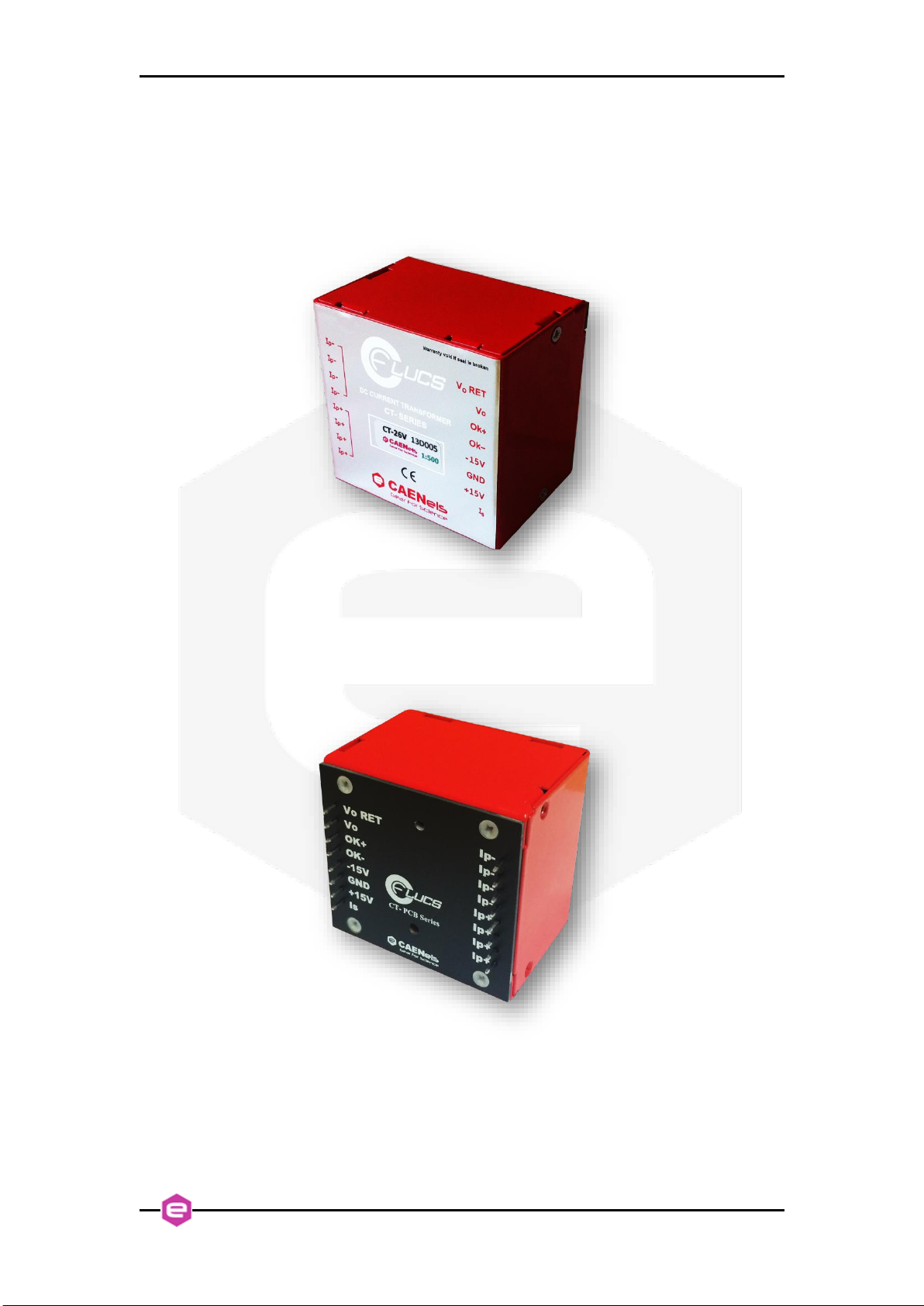
1.1 CT PCB Series Overview
The O-FLUCS < (O-FLUx Current Sensor) is based on a closed loop
technology that allows accurate and precise monitoring of DC and AC currents with
high bandwidth.
The metal casing guarantees higher noise immunity and reduces undesired noise
pick-up from external sources. The transducers CT-13 and CT-26 are PCB-mount
devices rated at maximum currents of 13A, 26A and 52A with primary to secondary
transformation ratio of 1:250, 1:500 and 1:1000 respectively. Galvanic isolation
between the primary and the secondary circuits allows to measure currents at a different
potential and simplifies interfacing if using the < as the feedback element of current
regulated power supplies.
Output from the < sensors can be chosen between two different versions:
standard secondary current output or buffered voltage output (low temperature
coefficient shunt resistor and low-noise amplifier are embedded in the CT-13V, CT-
26V and CT-52V versions).
Main characteristics of the < current transformers are negligible temperature
coefficient on the secondary output current, excellent linearity and extremely low noise.
DC current transformers represents the ideal replacement for systems where
Hall-effect sensors are used as current sensing elements and better performances are
needed.
The compact mechanical dimensions of this transducer series and its limited
weight allows easy mounting on printed circuit boards with a Through Hole (TH)
topology. A plastic cover is placed on the bottom side of the device to allow easier
mounting on the PCB.
Main application fields for these current transducers are precise and extremely
stable regulated power supplies and power inverters.
Due to the excellent characteristics, the O-FLUCS transformers can be used in
a variety of calibration, acceptance testing and quality control applications in the
industrial and automotive fields.

CT PCB Series User’s Manual Introduction
9
Commercially available versions of the PCB-mount O-FLUCS current
transformers are the current-output CT-13, CT-26 and CT-52 with their respective “V”
voltage-output versions CT-13V, CT-26V and CT-52V.
Top view of a sample of the O-FLUCS CT PCB Series current transducer is
presented in Figure 1.
Figure 1: Top view of a CT-26 O-FLUCS current transducer
Bottom view of the same current transducer, with pin connectors and warranty
seals visible, is presented in Figure 2.
Figure 2: Bottom view of a CT-26 O-FLUCS current transducer
All the CT PCB series transducers have the same mechanical dimensions and the
CT-13, CT-26 and CT-52 can be easily interchanged together.

Introduction CT PCB Series User’s Manual
10
1.2 CT PCB Models and Versions
The <CT PCB series of current transducer has three different models that
differ for primary current rating; each model is available in two different output
versions –i.e. secondary current-output (standard) or secondary voltage-output (“V”
version).
The different models and versions of the CT PCB series are summarized in the
following table (Table 1):
Product Code
Model
Description
WCT13XAAAAAA
CT-13
13 A Primary Current <, PCB-mounting
WCT13XLPAAAA
CT-13-LP
13 A Primary Current <, Low Profile, PCB-
mounting
WCT26XAAAAAA
CT-26
26 A Primary Current <, PCB-mounting
WCT52XAAAAAA
CT-52
52 A Primary Current <, PCB-mounting
WCT13VXAAAAA
CT-13V
13 A Primary Current <, PCB-mounting,
Voltage-Output
WCT26VXAAAAA
CT-26V
26 A Primary Current <, PCB-mounting,
Voltage-Output
WCT52VXAAAAA
CT-52V
52 A Primary Current <, PCB-mounting,
Voltage-Output
Table 1: CT-PCB series versions and models
On the rear side of the power supply unit are visible the air outlets for cooling,
output connection terminals, interlock and output status connector, three-phase inputs,
rail fuses and the analog output monitor coaxial connector.

CT PCB Series User’s Manual Installation and Operation
11
2.Installation and Operation
General considerations and description of pinout and recommended PCB layout
are herein presented.
2.1 Connections
Any transducer of the CT PCB series has 16-position pinout connections which
that is used to mount the device to a Printed Circuit Board (PCB). Not all of these
sixteen (16) pins are present in all versions, since the standard secondary current-output
version has different signals with respect to the “V” voltage-output version.
Please refer to the following Figure 3 and the following table –i.e. Table 2 –in
order to perform correct connections to the PCB for each model.
Figure 3: Pinout scheme of the CT PCB series transducers (top view)
Pin #1
Pin #8
Pin #9
Pin #16

Installation and Operation CT PCB Series User’s Manual
12
Pin #
CT-13 or CT-26
or CT-52
(Current Output)
CT-13V or CT-26V
or CT-52V
(Voltage Output)
1
Ip-
2
Ip-
3
Ip-
4
Ip-
5
Ip+
6
Ip+
7
Ip+
8
Ip+
9
IS
nc
10
+ 15 V
11
GND
12
-15 V
13
OK -
14
OK +
15
nc
Vo
16
nc
Vo RET
Table 2: Transducer pinouts
Please note that pins not present on the respective model and version are indicated
in Table 2 as nc = not connected. Please note that, internally, Is is directly connected
to GND.
2.2 Recommended PCB Footprint
In order to correctly place, mount and connect the CT current transducers to the
Printed Circuit Board (PCB), the recommended PCB footprint is represented in Figure
4(dimensions in mils) and Figure 5 (dimensions in mm).
Please note that, referring to Table 2, mounting holes for pin #15 and pin #16 can
be discarded for the CT-13, CT-26 and CT-52 transducers while hole for pin #9 can be
discarded when using the “V”-versions (CT-13V, CT-26V and CT-52V).

CT PCB Series User’s Manual Installation and Operation
13
Figure 4: Recommended PCB footprint (dimensions in mils)
Figure 5: Recommended PCB footprint (dimensions in mm)

Installation and Operation CT PCB Series User’s Manual
14
2.3 PCB Layout Guidelines
Since the primary flowing into the primary conductor can be as high as 52A for
the CT-52 and CT-52V models, it is necessary to correctly connect the current to be
measured to the input pins (#1 to #8).
The recommended PCB layout is herein shown in Figure 6.
Figure 6: Recommended PCB layout for primary conductor
It is highly recommended to make multiple planes/tracks on different PCB
layers in order to bring the primary current to the CT pins. The use of thermal reliefs
(30 mils) to allow easier soldering to the PCB is also strongly suggested.
NOTE: primary current needs to be shared equally among all input pins,
especially for high current values. Failure to do so may heat up the device to
excessive temperature values.
2.4 Secondary-side Signals
The signals on the “secondary” side of the CT current transducers are found from
pin #9 to pin #16 (please note that not all of them are present on all versions).
IP+
IP-

CT PCB Series User’s Manual Installation and Operation
15
2.4.1 Power Supply
Supply voltages for the CT have to be fed to pin #10 (+15V) and to pin #12 (-
15V); both these voltages are referred to pin #11 (GND) and have a rated tolerance of
±6% on the nominal values.
Maximum current that can be drawn from each one of these supply voltages is
of 100 mA.
2.4.2 Secondary Current
On the standard CT-13, CT-26 and CT-52 versions the secondary current output
IS, scaled by the current transformation ratio (1:250 for the CT-13, 1:500 for the CT-26
and 1:1000 for the CT-52), is found on pin #9.
Maximum secondary current is rated at ±52 mA and an external shunt resistor,
which can be placed close to the user’s desired measuring circuit, is needed in order to
convert the current signal to voltage.
The voltage output pins (VOand VORET) are not installed on CT-13, CT-26
and CT-52 versions.
2.4.3 Voltage Output (“V” versions only)
A buffered output voltage signal is present on the voltage output versions of the
CT- series –i.e. CT-13V, CT-26V and CT-52V transducer –in order to allow easier
connection of the DCCT to an external circuit or an Analog to Digital converter.
The full-scale output bipolar signal VO(pin #15) is referred to VORET(pin
#16) and the behavior is as follows:
•+10V output if the primary current is +12.5A (CT-13V), at +25A (CT-26V) or
at +50A (CT-52V);
•-10V output if the primary current is -12.5A (CT-13V), at -25A (CT-26V) or at
-50A (CT-52V).
This behavior can be resumed in the gain parameter G, in [V/A], expressed as
the ratio between the transducer output voltage
and the primary current IP.
This gain value is G = 0.8 V/A for the CT-13V version, G = 0.4 V/A for the
CT-26V version and G = 0.2 V/A for the CT-52V version.
VO RET pin is not internally connected to ground GND (pin #11) and it should
be connected to ground directly in a single-point connection (e.g. on an external ADC
ground pins or VIN- pin). The availability of this “return” signal is very useful in order

Installation and Operation CT PCB Series User’s Manual
16
to avoid additional ground-loop noise pickup on the voltage-output version of the
transducer.
Please note that the maximum differential voltage between the VO RET and
the GND pin has to be kept within ±0.5V.
In the voltage output “V”-version of the transducers the current output pin IS
(pin #9) is not present.
A screenshot of a primary 1A 20-kHz current sine-wave superimposed on a DC
current offset of 0.5A and the respective voltage output of a CT–13V transducer are
shown in Figure 7:
Figure 7: Primary current and voltage output (measured between pins VOand VORET)
Please note that output impedance for the “V”-version models is 50 Ω.
2.4.4 OK Signal
An OK signal, obtained from the outputs of an optocoupler phototransistor
(OK+ and OK-, pins #14 and #13 respectively) is present on all versions of the CT-
series. Please note that the OK- signal is not internally connected to the ground potential
and can be connected to an external reference potential.
A pull-up resistor is needed (between the OK+ and some supply voltage referred
to the OK- potential) in order to correctly obtained the correct signaling.
Two examples on how to connect the OK+ and OK- signals are hereafter
presented in Figure 8 and in Figure 9.
1 A
0.8 V

CT PCB Series User’s Manual Installation and Operation
17
Figure 8: OK signals connections using the +15V and the GND pins
Figure 9: OK signals connections as digital interfacing to +3.3V
Note that the connection scheme presented in Figure 8 is referred to the GND
potential and the OK_SIGNAL is at low level (<0.4V) if the CT transducer is correctly
working while it is at high level (>14.5V) when the transducer is not.
In the configuration presented in Figure 9, the current transducer can be easily
interfaced to a digital microcontroller, a Digital Signal Processor or an FPGA, supplied
by a +3.3V voltage source.
Please note that the +3.3V supply and the OK_SIGNAL is referred to DGND
potential, which can be the same or different from the GND potential on which the CT
device is supplied from. The OK_SIGNAL is found to be at low level (<0.4V) when
the transducer is correctly working and at high-level (>3V) when not.

Technical Specifications CT PCB Series User’s Manual
18
3.Technical Specifications
Technical specifications for < CT-13, CT-26 and CT-52 current transducers
(both current and voltage output versions) are herein presented.
Technical Specifications
CT-13
CT-26
CT-52
Current Transformation
Ratio - N
1:250
1:500
1:1000
Maximum DC Primary
Current - IP(DC)
±13 A
±26 A
±52 A
Maximum RMS Primary
Current - IP(RMS)
9.2 A
18.4 A
36.8 A
Current Polarity
Bipolar
Maximum DC Secondary
Current - IS(DC)
±52mA
Maximum RMS Secondary
Current - IS(RMS)
37 mA
External Shunt Resistor
Value - RS
0…40 Ω
Small Signal Bandwidth
(±3 dB) –typ. BW
500 kHz
200 kHz ("V"-version)
Equivalent Input Noise
(@Bandwidth) *
< 1 ppm/FS @ 200Hz
< 10 ppm/FS @ 50 kHz
Output Voltage
("V"-version) - VOUT
±10.4 V
Output Voltage Gain
("V"-version) - VOUT/IP(DC)
0.8 V/A
0.4 V/A
0.2 V/A
Maximum Output Current
("V"-version)
±15 mA
Temperature Coefficient -
TC
< 0.5 ppm/°C
typ. < 2 ppm/°C ("V"-version)
Non-Linearity
< 5 ppm
< 15 ppm ("V"-version)
Induction into Primary
(0-100 kHz) typ.
140 µV (RMS)
400 µV (RMS, LP
model)
70 µV (RMS)
35 µV (RMS)
Offset *
< 250 ppm / FS
< 10 ppm / FS (with factory calibration)
Protection Signal
OK Status
Supply Voltage (± 6%)
±15 V
Current Consumption
50 mA + IS

CT PCB Series User’s Manual Technical Specifications
19
Secondary Coil Resistance -
RSEC
42 Ω
Accuracy (typ.) *
< 30 ppm / FS
< 0.25% / FS (“V” - version)
Connections
16-pin through-hole PCB mounting
Operating Temperature
Range
0°C –50°C
0°C –50°C
0°C –40°C
Mechanical (Outer)
Dimensions
66 × 64 × 48 mm
Maximum Weight
300 g
* These specifications are guaranteed only when the CT sensor is used with the dedicated CAEN ELS PS1215 power supply
Table 3: Technical Specifications
3.1 Equivalent Input Noise
The typical equivalent input noise of the CT PCB transducer series is hereafter
presented as a function of the measuring bandwidth and of the model. The table and its
graph are valid for all models and for both current and voltage output options.
Equivalent Input Noise for CT-13 and CT-26 and CT-52
Bandwidth
Equivalent Input Noise (ppm/FS)
200 Hz
1.0
1 kHz
6.5
10 kHz
7.5
50 kHz
9.5
Table 4: Equivalent Input Noise (typical values)

Technical Specifications CT PCB Series User’s Manual
20
Figure 10: Equivalent Input Noise graph (typical values)
3.2 External Shunt Resistor
The maximum value of the external shunt resistor that can be connected on the
ISoutput pin in the current-output versions is shown hereafter in the following chart.
Figure 11: Maximum external shunt resistor (Current version only)
0
1
2
3
4
5
6
7
8
9
10
220 200 2000 20000
Equivalent Input Noise (ppm/FS)
Bandwidth (Hz)
100
110
120
130
140
150
160
170
180
190
200
210
220
230
240
250
260
30 35 40 45 50 55
Maximum Shunt Resistor [Ω]
IS[mA]
This manual suits for next models
7
Table of contents
Other Caen ELS Transducer manuals
Popular Transducer manuals by other brands

NK TECHNOLOGIES
NK TECHNOLOGIES VTU Series instructions

Fluke
Fluke PV350 instruction sheet

PICO
PICO WPS600 user guide

Simrad
Simrad 38-9 - REV B datasheet

Setra Systems
Setra Systems Multi-Sense 231RS operating instructions

S+S Regeltechnik
S+S Regeltechnik THERMASGARD TM54 Series Operating Instructions, Mounting & Installation

Veris
Veris PX3ULX05 Connection instructions

S+S Regeltechnik
S+S Regeltechnik RTM-CO2-2S Operating Instructions, Mounting & Installation

Mianyang Weibo Electronic
Mianyang Weibo Electronic WBI417S41 user manual

Desoutter
Desoutter AWT 1-6S User instructions

APAR
APAR AR250 User instruction

DaytonAudio
DaytonAudio HDN-8 user manual