Caen V791 User manual

Technical
Information
Manual
MOD. V 791
28 May 1999
Revision n. 2
32 CH. ICARUS
ANALOG BOARD
NPO:
00100/98:V791x.MUTx/02

&$(1
&$(1
Document type: Title: Revision date: Revision:
User's Manual (MUT) Mod. V791, ICARUS 32-channel analog board 27/05/99 2
NPO: Filename: Number of pages: Page:
00100/98:V791x.MUTx/02 V791MN4.DOC 17 2
TABLE OF CONTENTS
1. GENERAL DESCRIPTION.........................................................................................................................4
1.1. OVERVIEW ...............................................................................................................................................4
1.2. MAIN TECHNICAL SPECIFICATIONS ...........................................................................................................5
2. FUNCTIONAL DESCRIPTION..................................................................................................................6
3. TECHNICAL SPECIFICATIONS..............................................................................................................9
3.1. PACKAGING..............................................................................................................................................9
3.2. POWER REQUIREMENTS .........................................................................................................................11
3.3. EXTERNAL CONNECTIONS ......................................................................................................................11
3.3.1. INPUTS .........................................................................................................................................13
3.3.2. OUTPUTS .....................................................................................................................................14
3.4. DISPLAYS ...............................................................................................................................................14
4. HARDWARE SETTINGS..........................................................................................................................15
5. OUTPUT DATA..........................................................................................................................................17

&$(1
&$(1
Document type: Title: Revision date: Revision:
User's Manual (MUT) Mod. V791, ICARUS 32-channel analog board 27/05/99 2
NPO: Filename: Number of pages: Page:
00100/98:V791x.MUTx/02 V791MN4.DOC 17 3
LIST OF FIGURES
FIG. 2.1 - BLOCK DIAGRAM OF THE MODEL V791....................................................................................................6
FIG. 3.1 - MODEL V791 BOARD AND CONNECTORS ................................................................................................9
FIG. 3.2 - FRONT PANEL OF THE MODEL V791.......................................................................................................10
FIG. 3.3 - PIN CONFIGURATION OF THE CONNECTORS ON THE MODEL V791..........................................................12
FIG. 4.1 - COMPONENT LOCATION ON THE MODEL V791 BOARD...........................................................................16
FIG. 5.1 - FORMAT OF THE OUTPUT DATA PACKET ................................................................................................17
LIST OF TABLES
TABLE 1.1 - MODEL V791C AND MODEL V791Q MAIN TECHNICAL SPECIFICATIONS..............................................5
TABLE 3.1 - POWER REQUIREMENTS......................................................................................................................11

&$(1
&$(1
Document type: Title: Revision date: Revision:
User's Manual (MUT) Mod. V791, ICARUS 32-channel analog board 27/05/99 2
NPO: Filename: Number of pages: Page:
00100/98:V791x.MUTx/02 V791MN4.DOC 17 4
1. General description
1.1. Overview
The CAEN Model V791 is a 32-channel analog board designed for optimum performance
as front-end electronics for the ICARUS experiment (see, for example, the web site:
www.aquila.infn.it:80/icarus/
). Its function is to digitize the signals coming from the
detector and transmit them via a fast serial link. The V791 module can adapted to any
detector which uses a charge (or current) preamplifier in Radeka configuration (folded
cascode). For further details about how to adapt the module, please contact the factory
directly.
A functional block of the V791 module is shown in Fig. 2.1. The 32 input signals are sent
to 32 low-noise preamplifiers and relevant shapers. The processed signals are then
multiplexed and digitized in order to be transmitted via the serial link.
The section for the signal digitization consists of four 8-channel blocks. Each block is
made of two 4-channel analog multiplexers and a 20 MHz ADC. Each channel is sampled
at a 2.5 Ms/s rate and digitized with a 10-bit resolution by using a time division
multiplexing technique. The maximum delay between the sampling of a channel and the
following one is 400 ns.
The Model V791 is housed in a 1-unit wide, 6-unit high Eurocard mechanics with special
shielding for the protection of the low-noise circuits.
The module hosts four external connectors:
•a 64-pin input connector (rear panel),
•a 30-pin power supply and auxiliary signal connector (rear panel),
•a serial link connector (front panel),
•a Σ
out connector (front panel).
Please note that, although the module is housed in a Eurocard standard mechanics, the
rear connectors are not VME standard connectors since the backplane for which the
board has been designed is proprietary.
Two different version are available, specifically the Mod. V791C and the Mod. V791Q
which, respectively, allow for the digitalisation of the input current and the digitalisation of
the input charge. These two version differ only for the values of the components mounted
near the preamplifiers and the shapers. The main technical specifications of both
versions are reported in Table 1.1.

&$(1
&$(1
Document type: Title: Revision date: Revision:
User's Manual (MUT) Mod. V791, ICARUS 32-channel analog board 27/05/99 2
NPO: Filename: Number of pages: Page:
00100/98:V791x.MUTx/02 V791MN4.DOC 17 5
1.2. Main technical specifications
Table 1.1 - Model V791C and Model V791Q main technical specifications
Parameter Mod. V791C Mod. V791Q
Number of channels 32 32
Resolution 10 bits 10 bits
Sampling frequency 2.5 MHz 2.5 MHz
Input sensitivity 10 ± 10% count/nA 3.3 ± 10% count/fC
Input signals 1 nA x 3 µs±3fC
Output data 10-bit double data, 40MHz 10-bit double data, 40MHz
Noise (RMS) < 2 LSB (*) < 2 LSB (*)
S/N (charge) > 10 > 6
Input range 100 ± 10% nA 300 ± 10% fC
Test pulse input range ± 2.5 Vpp ± 2.5 Vpp
Sampling rate 400 ns/channel 400 ns/channel
Preamp. Transconductance 5.6 MΩ// 0.15 pF 100 MΩ// 0.5 pF
Preamplifier time constant 1 µs 50 µs
First shaper time constant 1 µs 0.27 µs
Second shaper time constant 1 µs-
First adder time constant 1 µs1µs
Second adder time constant 1 µs1µs
Adder sensitivity (DC) 1 mV/count 1 mV/count
Offset (count) ± 10 (external setting) ± 10 (external setting)
Crosstalk (dB) < -40 dB < -40 dB
(*) Noise measured @ Detector Capacitance = 400 pF.

&$(1
&$(1
Document type: Title: Revision date: Revision:
User's Manual (MUT) Mod. V791, ICARUS 32-channel analog board 27/05/99 2
NPO: Filename: Number of pages: Page:
00100/98:V791x.MUTx/02 V791MN4.DOC 17 6
2. Functional description
& ADC
Fast OpAmp
& ADC
Fast OpAmp
A
B
Digital
Multiplexer
2:1
10
& ADC
Fast OpAmp
& ADC
Fast OpAmp
A
B
10
Output Link
DS90CR213
SYNC
21
CKLINK
Control
Logic
MAX7032
10
Attenuator
40 dB
Attenuator
40 dB
Rx
Power supply
+1
INA
B_CLK
/
B_CLK
VDAC
+TPULSE
-TPULSE
TPO_EN
TPE_EN
40 MHz
C8
C10
C12
C14
C1
C3
C5
C7
C9
C11
C13
C15
C16
C18
C20
C22
C24
C26
C28
C30
C17
C19
C21
C23
C25
C27
C29
C31
P3
P1
Link
Conn
Pre
Pre
Pre
Pre
C0
C2
C4
C6
Multiplexer
4:1
AD8184
Pre
Pre
Pre
Pre
Multiplexer
4:1
AD8184
Pre
Pre
Pre
Pre
Multiplexer
4:1
AD8184
Pre
Pre
Pre
Pre
Multiplexer
4:1
AD8184
Pre
Pre
Pre
Pre
Multiplexer
4:1
AD8184
Pre
Pre
Pre
Pre
Multiplexer
4:1
AD8184
Pre
Pre
Pre
Pre
Multiplexer
4:1
AD8184
Pre
Pre
Pre
Pre
Multiplexer
4:1
AD8184
out
Acq on
Shaper
Shaper
Shaper
Shaper
Shaper
Shaper
Shaper
Shaper
Shaper
Shaper
Shaper
Shaper
Shaper
Shaper
Shaper
Shaper
Shaper
Shaper
Shaper
Shaper
Shaper
Shaper
Shaper
Shaper
Shaper
Shaper
Shaper
Shaper
Shaper
Shaper
Shaper
Shaper
C
O
N
N
E
C
T
O
R
I
N
P
U
T
Digital
Multiplexer
2:1
C
O
N
N
E
C
T
O
R
O
U
T
P
U
T
C
O
N
N
E
C
T
O
R
P
O
W
E
R
S
U
P
P
L
Y
Fig. 2.1 - Block diagram of the Model V791

&$(1
&$(1
Document type: Title: Revision date: Revision:
User's Manual (MUT) Mod. V791, ICARUS 32-channel analog board 27/05/99 2
NPO: Filename: Number of pages: Page:
00100/98:V791x.MUTx/02 V791MN4.DOC 17 7
Fig. 2.1 shows a detailed block diagram of the V791 module.
The first section, constituted by the preamplifiers and the shapers, provides the
conversion from current to voltage of the input signals and their shaping. The current
signals coming from the detector are converted into voltage signals by the preamplifiers.
These are constituted by two JFET followed by an ASIC specially developed by CAEN
Microelectronics. The output voltage signals are then sent to the shapers having two
1-µsec time constants or one 0.27-µsec time constant for the Mod. V791C and
Mod. V791Q, respectively. In order to allow a check of the channel operation the
preamplifiers have a test input coupled through a 1-pF capacitor.
The signals coming out the shapers are sent to the input of the analog multiplexers in
such an order as to keep the same signal sequence of the input connector. Moreover, the
Σout output connector on the front panel provides the sum of all the shaper outputs.
The second section is constituted by four blocks, each controlling 8 channels. Each block
comprehends two analog multiplexers, a fast operational amplifier and an ADC which is
connected to the input of the digital multiplexer. The 8-channel block connected to the
input A of the digital multiplexer relates to the odd channels, while that connected to the
input B relates to the even ones.
The parallel-connected outputs of the analog multiplexer are amplified by the fast
operational amplifier which has also the function of shifting the ADC baseline by adding a
DC level. The external DAC (VDAC control signal) allows to set this baseline correctly,
according to the type of signal to be converted. The operational amplifier has as well a
capacitor which can be used for limiting the bandwidth in order to reduce the noise,
although this implies a deterioration of the cross-talk. This can be done via hardware by
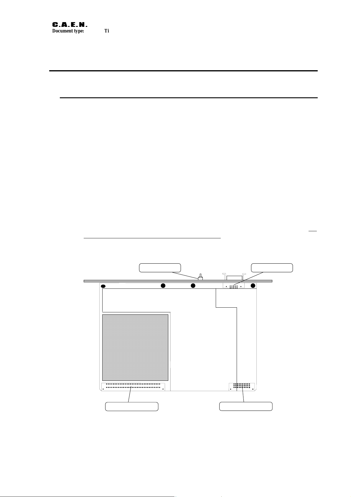
soldering a capacitor on the printed board (capacitor CBL on the printed board; please
refer to Fig. 4.1).
The ADC is a 10-bit 20-MHz converter with external references.
The third section is the digital one and comprehends the digital multiplexers, the control
logic and the output link.
The control logic, hosted in a PAL device (MAX7032-15), generates the multiplexing and
digitizing signals which are sent through the digital multiplexer to the input of the 40-MHz
serial link.
The external control signals accepted by the module are VDAC, +TPULSE, -TPULSE,
TPE_EN, TPO_EN, B_CLK, /B_CLK and EN_BRD.
The VDAC control signal allows to set the baseline to be added to the input of the fast
operational amplifier, according to the type of signal to be converted.
The differential test pulse (+TPULSE and -TPULSE signals) comes from the backplane.
The signal coming from the backplane has to be attenuated by a factor 10 before being
sent to the preamplifiers.
The TPE_EN and TPO_EN signals allow to enable the test pulsing on the even and odd
channels, respectively. Since the test pulse is directly connected to the input of the
preamplifiers, when the test pulse is not used, it is necessary to connect it to ground
through a very low impedance by disabling the TPE_EN and TPO_EN signals.
The differential clock signal (B_CLK and /B_CLK) is the external clock used to
synchronise all the V791 modules in the crate. The selection of the clock, external or
internal, can be made by means of a soldering (soldering pad S2 on the printed board;
please refer to Fig. 4.1). The external clock is the default setting.
The EN_BRD logic signal is used to force the control logic in the reset state and,
consequently, to stop the digitization of the signals.
All these control signals are sent to the board via the relevant pins of the power supply
connector.

&$(1
&$(1
Document type: Title: Revision date: Revision:
User's Manual (MUT) Mod. V791, ICARUS 32-channel analog board 27/05/99 2
NPO: Filename: Number of pages: Page:
00100/98:V791x.MUTx/02 V791MN4.DOC 17 8
Moreover, a further output signal (RTXPWS) of the output connector
Link Conn
has been
foreseen to supply +5 V to a possible, external optical decoupler used to break the ground
loop. This can be done by making a solder on an appropriate pad in the printed board (S1
soldering pad, please refer to Fig. 4.1).
The output serial link features a 21-bit data word which is composed as follows:
•10-bit ADC datum coming, in turn, from one of the channels 0-15;
•10-bit ADC datum coming, in turn, from one of the channels 16-31;
•1-bit SYNC datum for the synchronisation of the signals.
The transmission sequence is such that each couple of 10-bit ADC data is relative to the
channels n and n + 16, with n running from 0 to 15. The SYNC bit is set to 1 in
correspondence with the couple of ADC data relative to the channels 15 and 31.

&$(1
&$(1
Document type: Title: Revision date: Revision:
User's Manual (MUT) Mod. V791, ICARUS 32-channel analog board 27/05/99 2
NPO: Filename: Number of pages: Page:
00100/98:V791x.MUTx/02 V791MN4.DOC 17 9
3. Technical Specifications
3.1. Packaging
The board is housed in a 1-unit wide, 6-unit high Eurocard standard mechanics.
The front panel of the Model V791 is shown in Fig. 3.2.
The module hosts four external connectors:
rear part of the module
: 64-pin input connector;
30-pin power supply and auxiliary signal connector;
front panel
: serial link output connector (Link Conn);
Σout output connector.
Fig. 3.1 shows the location of the connectors on the board and the three main functional
sections:
•preamplifier and shaper section,
•ADC and analog multiplexer section,
•digital section.
Please note that, although the module is housed in a Eurocard standard mechanics, the
rear connectors are not VME standard connectors since the backplane for which the
board has been designed is proprietary.
Input connector
a
b
c
a
b
c
a
b
c
ADC+MUX
SECTION
PREAMPLIFIER AND SHAPER
SECTION (SHIELDED) DIGITAL
SECTION
Power supply connector
Output connector
P1
P3
Link Conn
Output connector
Σout
Fig. 3.1 - Model V791 board and connectors

&$(1
&$(1
Document type: Title: Revision date: Revision:
User's Manual (MUT) Mod. V791, ICARUS 32-channel analog board 27/05/99 2
NPO: Filename: Number of pages: Page:
00100/98:V791x.MUTx/02 V791MN4.DOC 17 10
32 CH
ICARUS
DIGITIZER
Mod.
V791
L
I
N
K
40 MHz output
serial link
ACQ
ON
Σ
OUT
Acquisition On
LED
Σ
out
output
connector
Fig. 3.2 - Front panel of the Model V791

&$(1
&$(1
Document type: Title: Revision date: Revision:
User's Manual (MUT) Mod. V791, ICARUS 32-channel analog board 27/05/99 2
NPO: Filename: Number of pages: Page:
00100/98:V791x.MUTx/02 V791MN4.DOC 17 11
3.2. Power Requirements
The power requirements of the board are:
Table 3.1 - Power requirements
Power Supply Section Absorption (max)
+5 V analog 1 A
+5 V digital 1.2 A
-5 V analog 0.25 A
The crate must have a low-noise linear power supply with separate analog and digital
supply sections. It is suggested the use of a π-filter regulator for the analog section.
The board has three common terminals: AGND, AGND1, DGND. AGND refers to the
preamplifiers, AGND1 refers to the analog multiplexers, shapers and ADCs and DGND is
the common terminal of the digital section. The Σout output signal is referred to the
AGND1 common terminal.
3.3. External connections
The external connection pin configurations of the V791 module are shown in Fig. 3.3,
while their function and electro-mechanical specifications are listed in the following
sections.

&$(1
&$(1
Document type: Title: Revision date: Revision:
User's Manual (MUT) Mod. V791, ICARUS 32-channel analog board 27/05/99 2
NPO: Filename: Number of pages: Page:
00100/98:V791x.MUTx/02 V791MN4.DOC 17 12
1C
VCCD
VCCD
B_CLK
/
B_CLK
DGND
1A 1BIN0
IN1
IN2
IN3
AGND
AGND
AGND
AGND
1C 1A
IN4
IN5
IN6
IN7
IN8
IN9
AGND
AGND
AGND
AGND
AGND
AGND VEEA
VEEA1
VDAC
TPO_EN
DGND
AGND1
AGND1
VCCA1
VCCA
+TPULSE
-TPULSE
TPE_EN
AGND1
AGND
AGND
IN10
IN11
IN12
IN13
IN14
IN15
AGND
AGND
AGND
AGND
AGND
AGND
IN16
IN17
IN18
IN19
IN20
IN21
AGND
AGND
AGND
AGND
AGND
AGND
POWER SUPPLY
CONNECTOR (P1)
TX2
/
TX2
OUTPUT CONNECOTR
DGND
TX1
/
TX1
DGND
TX0
/
TX0
IN22
IN23
IN24
IN25
IN26
IN27
AGND
AGND
AGND
AGND
AGND
INPUT CONNECTOR
IN28
IN29
IN30
IN31
AGND
AGND
AGND
AGND
AGND
(Link Conn)
(P3)
EN_BRD
DGND
CKX
/
CKX
RTX_PWS
Fig. 3.3 - Pin configuration of the connectors on the Model V791

&$(1
&$(1
Document type: Title: Revision date: Revision:
User's Manual (MUT) Mod. V791, ICARUS 32-channel analog board 27/05/99 2
NPO: Filename: Number of pages: Page:
00100/98:V791x.MUTx/02 V791MN4.DOC 17 13
3.3.1. INPUTS
INPUT CONNECTOR (P3)
Mechanical specifications:
64-pin, C-type, A/C lines, DIN41612 standard connector;
Electrical specifications:
•AIN0..AIN31: analog inputs referring to the channels 0..31;
•AGND: common terminal of the analog inputs.
POWER SUPPLY CONNECTOR (P1)
Mechanical specifications:
30-pin, C-type, A/B/C lines, DIN41612 standard connector;
Electrical specifications:
•VCCD: +5V for the digital section;
•VCCA: +5V for the preamplifiers;
•VCCA1: +5V for the shapers and the analog multiplexer and ADC section;
•VEEA: -5V for the preamplifier;
•VEEA1: -5V for the analog multiplexer and shapers;
•DGND: common terminal of the digital section;
•AGND: common terminal of the preamplifiers;
•AGND1: common terminal of the shapers, analog multiplexers and ADCs;
•B_CLK: 40 MHz clock coming from the backplane, differential LVDS;
•/B_CLK: 40 MHz clock coming from the backplane, differential LVDS, inverted
phase;
•VDAC: setting voltage of the baseline (in the range ±2.5 V);
•TPO_EN: test pulse enable for the odd channels, TTL;
•TPE_EN: test pulse enable for the even channels, TTL;
•TPULSE: test pulse signal; this signal must be trapezoidal and have edge
amplitude and width so as to inject the desired current through a 1-pF
capacitor after a 1:11-attenuation. Optionally, the test signal can be
generated externally according to the test method used in the
experiment;
•-TPULSE: test pulse signal, inverted phase;
•EN_BRD: as long as it is high, the V791 Logic is forced in the reset state, TTL.

&$(1
&$(1
Document type: Title: Revision date: Revision:
User's Manual (MUT) Mod. V791, ICARUS 32-channel analog board 27/05/99 2
NPO: Filename: Number of pages: Page:
00100/98:V791x.MUTx/02 V791MN4.DOC 17 14
3.3.2. OUTPUTS
OUTPUT CONNECTOR (LINK CONN)
Mechanical specifications:
N102145212JL-type, Mini D ribbon connector.
Electrical specifications:
•TX0..TX2: data output of the digital link;
•/TX0../TX2: data output of the digital link, inverted phase;
•CKX: clock output of the digital link;
•/CKX: clock output of the digital link, inverted phase;
•DGND: common terminal for the digital link outputs;
•RTXPWS: power supply for a possible optical decoupler.
ANALOG ADDER OUTPUT CONNECTOR (ΣOUT)
Mechanical specifications:
SMB connector.
Electrical specifications:
•ΣOUT: sum of the outputs of all the shapers.
WARNING: the Σout output signal is referred to the shaper ground (AGND1) and,
consequently, the user must be very careful to avoid ground loops.
CAUTION
ΣΣ
OUT
IS REFERRED TO THE SHAPER GROUND (
AGND1
COMMON TERMINAL)
AND CONSEQUENTLY, IF
ΣΣ
OUT
IS USED,
THE USER MUST BE VERY CAREFUL TO AVOID GROUND LOOPS!
3.4. Displays
ACQ ON:
Colour:
red.
Function:
it lights up during data acquisition.

&$(1
&$(1
Document type: Title: Revision date: Revision:
User's Manual (MUT) Mod. V791, ICARUS 32-channel analog board 27/05/99 2
NPO: Filename: Number of pages: Page:
00100/98:V791x.MUTx/02 V791MN4.DOC 17 15
4. Hardware settings
The hardware settings described in the following are foreseen for both the versions,
nominally the Mod.V791C and the Mod.V791Q.
Selection of the clock source (external/internal):
it is performed by using the relevant soldering jumper pad (S2) placed on the PCB (refer
to Fig. 4.1):
•Soldering placed in Position A (high position, EXT):
Æ
external clock selected;
•Soldering placed in Position B (low position, INT):
Æ
internal clock selected.
The default setting is external clock.
Generation of the RTXPWS power supply:
the RTXPWS output signal is used to supply +5 V to a possible external optical decoupler
which can be used to break the ground loop. The RTXPWS power supply is provided at
the relevant pin of the output connector (LINK CONN) when a soldering is performed on
the relevant soldering pad (S1) placed on the PCB (refer to Fig. 4.1):
•No Soldering:
Æ
no RTXPWS power supply on the LINK connector;
•Soldering on the S2 pad:
Æ
the RTXPWS power supply is present on the relevant
pin of the LINK connector.
By default there is no soldering on the S2 pad.
Limitation of the Op-Amp bandwidth:
the PCB houses four empty pads(refer to Fig. 4.1), one for each Op-Amp, which allow to
solder an additional capacitor CBL to reduce the bandwidth of the relevant Op-Amp:
•No CBL capacitor:
Æ
default Op-Amp bandwidth;
•C
BL capacitor soldered on the pad:
Æ
the bandwidth of the relevant Op-Amp is
reduced.
By default there is no capacitor soldered on the pad.

&$(1
&$(1
Document type: Title: Revision date: Revision:
User's Manual (MUT) Mod. V791, ICARUS 32-channel analog board 27/05/99 2
NPO: Filename: Number of pages: Page:
00100/98:V791x.MUTx/02 V791MN4.DOC 17 16
EXT
CLK
INT
Position A (default)
:
External clock
selected
Position B
:
Internal clock
selected
EXT
CLK
INT
S2
INT
CLK
EXT
31 30
29 28
27 26
25 24
23 22
21 20
19 18
17 16
15 14
13 12
11 10
9 8
7 6
5 4
3 2
1 0
CH
CH
CH
CH
CH
CH
CH
CH
1
No soldering (default)
:
no RTXPWS
p
ower su
pp
l
y
on the LINK
connector
S1
Soldering:
the RTXPWS
p
ower su
pp
l
y
is
p
resent
on the LINK connector
No capacitor (default)
:
Default O
p
-Am
p
bandwidth
C
BL
C
BL
capacitor inserted:
O
p
-Am
p
bandwidth limited
Fig. 4.1 - Component location on the Model V791 board

&$(1
&$(1
Document type: Title: Revision date: Revision:
User's Manual (MUT) Mod. V791, ICARUS 32-channel analog board 27/05/99 2
NPO: Filename: Number of pages: Page:
00100/98:V791x.MUTx/02 V791MN4.DOC 17 17
5. Output data
The data at the serial link output are 21-bit words and are structured as follows (refer to
Fig. 5.1):
•10 bits containing the ADC datum of the channel n,
•10 bits containing the ADC datum of the channel n + 16,
•1 bit containing the SYNC signal,
with n running from 0 to 15.
The SYNC bit (Bit 20 in the figure) is set to 1 in correspondence with the couple of ADC
data relative to the channels 15 and 31 (n = 15).
CHANNEL 0CHANNEL 16
0
CHANNEL 1CHANNEL 17
0
CHANNEL 2CHANNEL 18
0
CHANNEL 3CHANNEL 19
0
CHANNEL 4CHANNEL 20
0
CHANNEL 5CHANNEL 21
0
CHANNEL 6CHANNEL 22
0
CHANNEL 7CHANNEL 23
0
CHANNEL 8CHANNEL 24
0
CHANNEL 9CHANNEL 25
0
CHANNEL 10CHANNEL 26
0
CHANNEL 11CHANNEL 27
0
CHANNEL 12CHANNEL 28
0
CHANNEL 13CHANNEL 29
0
CHANNEL 14CHANNEL 30
0
CHANNEL 15CHANNEL 31
1
Bit
20 Bits 19...10 Bits 9...0
Fig. 5.1 - Format of the output data packet
This manual suits for next models
2
Table of contents
Other Caen Media Converter manuals
Popular Media Converter manuals by other brands

Cross Technologies
Cross Technologies 3116-192 instruction manual

Tascam
Tascam SB-16D owner's manual

Grandbeing
Grandbeing SH0101-002 operating instructions

GPX
GPX HM3817DTBLK instruction manual

Advanced Technology International USA
Advanced Technology International USA QSP-660 Owner's manual & operating instructions

Stradis
Stradis HDM500 user guide