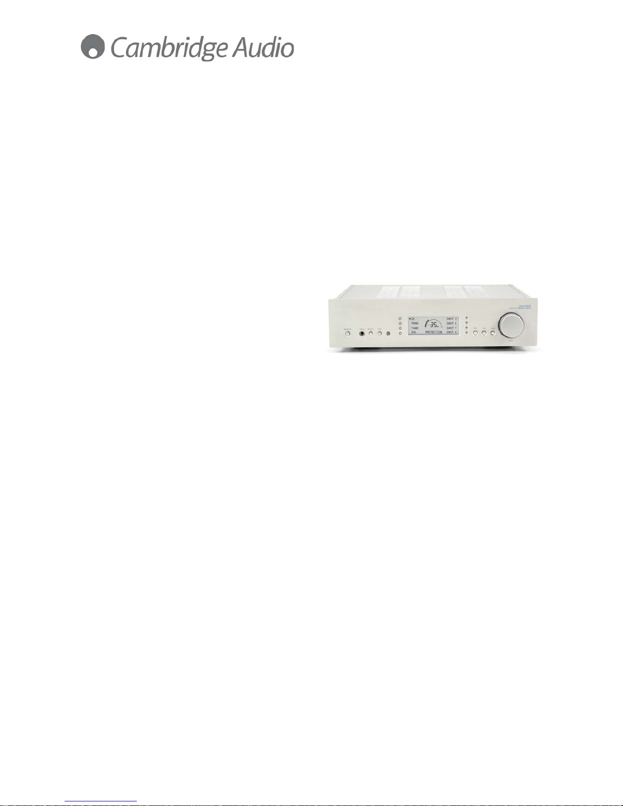
Cambridge Audio azur 840A Quick reference guide
Other Cambridge Audio Amplifier manuals

Cambridge Audio
Cambridge Audio cp2 User manual

Cambridge Audio
Cambridge Audio AZUR 550A User manual

Cambridge Audio
Cambridge Audio CXA81 User manual

Cambridge Audio
Cambridge Audio AXA35 User manual

Cambridge Audio
Cambridge Audio Azur 540A V2.0 User manual

Cambridge Audio
Cambridge Audio Alva Solo User manual

Cambridge Audio
Cambridge Audio Azur 540A V2 User manual

Cambridge Audio
Cambridge Audio 851E User manual

Cambridge Audio
Cambridge Audio Azur 540A V2 User manual

Cambridge Audio
Cambridge Audio AXA25 User manual

Cambridge Audio
Cambridge Audio Azur 540A User manual

Cambridge Audio
Cambridge Audio azur 350A User manual

Cambridge Audio
Cambridge Audio AZUR 650A User manual

Cambridge Audio
Cambridge Audio azur 651 W User manual

Cambridge Audio
Cambridge Audio AZUR 840A V2 User manual

Cambridge Audio
Cambridge Audio Integrated Amplifier Azur 740A User manual

Cambridge Audio
Cambridge Audio AZUR 651A User manual

Cambridge Audio
Cambridge Audio C10974 User manual

Cambridge Audio
Cambridge Audio Azur 340A User manual

Cambridge Audio
Cambridge Audio EDGE A User manual