Chimei N150X3-L09 User manual
RGB ELEKTRONIKA AGACIAK CIACIEK
SPÓŁKA JAWNA
Jana Dlugosza 2-6 Street
51-162 Wrocław
Poland
biuro@rgbelektronika.pl
+48 71 325 15 05
www.rgbautomatyka.pl
www.rgbelektronika.pl
DATASHEET
www.rgbautomatyka.pl
www.rgbelektronika.pl
OTHER SYMBOLS:
N150X3-L09
N150X3L09, N150X3 L09, N150X3-L09
CHI MEI

YOUR
PARTNER IN
MAINTENANCE
At our premises in Wrocław, we have a fully equipped servicing facility. Here we perform all the repair
works and test each later sold unit. Our trained employees, equipped with a wide variety of tools and
having several testing stands at their disposal, are a guarantee of the highest quality service.
OUR SERVICES
ENCODERS
SERVO
DRIVERS
LINEAR
ENCODERS
SERVO AMPLIFIERS
CNC
MACHINES
MOTORS
POWER
SUPPLIERS
OPERATOR
PANELS
CNC
CONTROLS
INDUSTRIAL
COMPUTERS
PLC
SYSTEMS
Repair this product with RGB ELEKTRONIKA ORDER A DIAGNOSIS ∠
Buy this product at RGB AUTOMATYKA BUY ∠

www.DataSheet.net/
Datasheet pdf - http://www.DataSheet4U.co.kr/
Issued Date: Sep.27, 2005
Model No.: N150X3 - L09
Approval
2 / 27
Version 2.2
- CONTENTS -
REVISION HISTORY ------------------------------------------------------- 3
1. GENERAL DESCRIPTION ------------------------------------------------------- 4
1.1 OVERVIEW
1.2 FEATURES
1.3 APPLICATION
1.4 GENERAL SPECIFICATIONS
1.5 MECHANICAL SPECIFICATIONS
2. ABSOLUTE MAXIMUM RATINGS ------------------------------------------------------- 5
2.1 ABSOLUTE RATINGS OF ENVIRONMENT
2.2 ELECTRICAL ABSOLUTE RATINGS
2.2.1 TFT LCD MODULE
2.2.2 BACKLIGHT UNIT
3. ELECTRICAL CHARACTERISTICS ------------------------------------------------------- 6
3.1 TFT LCD MODULE
3.2 BACKLIGHT UNIT
3.3 EDID DATA
4. BLOCK DIAGRAM ------------------------------------------------------- 13
TFT LCD MODULE w/ INVERTER
5. INPUT TERMINAL PIN ASSIGNMENT ------------------------------------------------------- 13
5.1 TFT LCD MODULE
5.2 TIMING DIAGRAM OF LVDS INPUT SIGNAL
5.3 COLOR DATA INPUT ASSIGNMENT
6. INTERFACE TIMING ------------------------------------------------------- 16
6.1 INPUT SIGNAL TIMING SPECIFICATIONS
6.2 POWER ON/OFF SEQUENCE
7. OPTICAL CHARACTERISTICS ------------------------------------------------------- 18
7.1 TEST CONDITIONS
7.2 OPTICAL SPECIFICATIONS
8. PRECAUTIONS ------------------------------------------------------- 23
8.1 ASSEMBLY AND HANDLING PRECAUTIONS
8.2 SAFETY PRECAUTIONS
9. DEFINITION OF LABELS ------------------------------------------------------- 24
9.1 CMO MODULE LABEL
9.2 Dell LABEL
10.2.1 MAL PPID LABEL
10.2.2 CARTON LABEL
10.2.3 PALLET LABEL
10. PACKING ------------------------------------------------ 25
10.1 CARTON
10.2 PALLET
www.DataSheet.net/
Datasheet pdf - http://www.DataSheet4U.co.kr/
Issued Date: Sep.27, 2005
Model No.: N150X3 - L09
Approval
3 / 27
Version 2.2
REVISION HISTORY
Version Date Page
(New) Section Description
Ver 1.0
Ver 2.0
Ver 2.1
Ver 2.2
Jan.31 ‘05
May.23 ’05
Aug.31 ‘05
Sep 27,’05
All
9
25
14
15
All
3.3
10
4.2
5.1
Perminaliary specification was first issued
Added EDID code
Modified Carton & pallet
Added 4.2 BLU unit
Modified pin assignment
www.DataSheet.net/
Datasheet pdf - http://www.DataSheet4U.co.kr/

Issued Date: Sep.27, 2005
Model No.: N150X3 - L09
Approval
4 / 27
Version 2.2
1. GENERAL DESCRIPTION
1.1 OVERVIEW
N150X3- L09 is a 15.0” TFT Liquid Crystal Display module. This module supports 1024 x 768 XGA mode
and can display 262,144 colors. The optimum viewing angle is at 6 o’clock direction.
1.2 FEATURES
- Thin and Light Weight
- XGA (1024 x 768 pixels) resolution
- DE only mode
- 3.3V LVDS (Low Voltage Differential Signaling) interface with 1 pixel/clock
- SPWG (Standard Panel Working Group) Style B compatible
- Single CCFL
- ROHS product
1.3 APPLICATION
- TFT LCD Notebook
1.4 GENERAL SPECIFICATI0NS
Item Specification Unit Note
Active Area 304.1 (H) x 228.1 (V) (15.0” diagonal) mm
Bezel Opening Area 307.8 (H) x 231.6 (V) mm (1)
Driver Element a-si TFT active matrix - -
Pixel Number 1024 x R.G.B. x 768 pixel -
Pixel Pitch 0.297 (H) x 0.297 (V) mm -
Pixel Arrangement RGB vertical stripe - -
Display Colors 262,144 color -
Transmissive Mode Normally white - -
Surface Treatment Hard coating (3H), Anti-glare (Haze 25) - -
1.5 MECHANICAL SPECIFICATIONS
Item Min. Typ. Max. Unit Note
Horizontal(H) 316.8 317.3 317.8 mm (1)
Vertical(V) 241.5 242 242.5 mm (1)
Module Size
Depth(D) - 5.7 6.0 mm (1)
Weight - 550 565 g -
Note (1) Please refer to the attached drawings for more information of front and back outline dimensions.
www.DataSheet.net/
Datasheet pdf - http://www.DataSheet4U.co.kr/

Issued Date: Sep.27, 2005
Model No.: N150X3 - L09
Approval
5 / 27
Version 2.2
2. ABSOLUTE MAXIMUM RATINGS
2.1 ABSOLUTE RATINGS OF ENVIRONMENT
Value
Item Symbol Min. Max.
Unit Note
Storage Temperature TST -20 +60 ºC (1)
Storage Humidity HST 10 90 %RH (1)
Operating Ambient Temperature TOP 0 +50 ºC (1), (2)
Operating Ambient Humidity HOP 20 90 %RH (1)
Shock (Non-Operating) SNOP - 200/2 G/ms (3), (4), (5)
Vibration (Non-Operating) VNOP - 1.5/10-200 G/Hz (4), (5)
Note (1) (a) 90 %RH Max. (Ta ≦40 ºC).
(b) Wet-bulb temperature should be 39 ºC Max. (Ta > 40 ºC).
(c) No condensation.
Note (2) The temperature of panel surface should be 0℃min. and 50 ℃max.
Note (3) Condition for 200/2 G/ms is Half Since Wave.
Note (4) The fixing condition is shown as below:
Note (5) At testing Vibration and Shock, the fixture in holding the module has to be hard and rigid enough
so that the module would not be twisted or bent by the fixture.
Side Mount Fixing Screw
Side Mount Fixing Screw
Sta
g
e
Bracket
LCD Module
gap=2mm
www.DataSheet.net/
Datasheet pdf - http://www.DataSheet4U.co.kr/
Issued Date: Sep.27, 2005
Model No.: N150X3 - L09
Approval
6 / 27
Version 2.2
2.2 ELECTRICAL ABSOLUTE RATINGS
2.2.1 TFT LCD MODULE
Value
Item Symbol
Min. Max.
Unit Note
Power Supply Voltage VCC -0.3 +4.0 V
Logic Input Voltage VIN -0.3 VCC+0.3 V (1)
2.2.2 BACKLIGHT UNIT
Value
Item Symbol
Min. Max.
Unit Note
Lamp Voltage VL- (2.5K) VRMS (1), (2), IL= 6.0 mA
Lamp Current IL2.0 6.5 mARMS
Lamp Frequency FL50 80 KHz (1), (2)
Note (1) Permanent damage to the device may occur if maximum values are exceeded. Function operation
should be restricted to the conditions described under Normal Operating Conditions.
Note (2) Specified values are for lamp (Refer to 3.2 for further information).
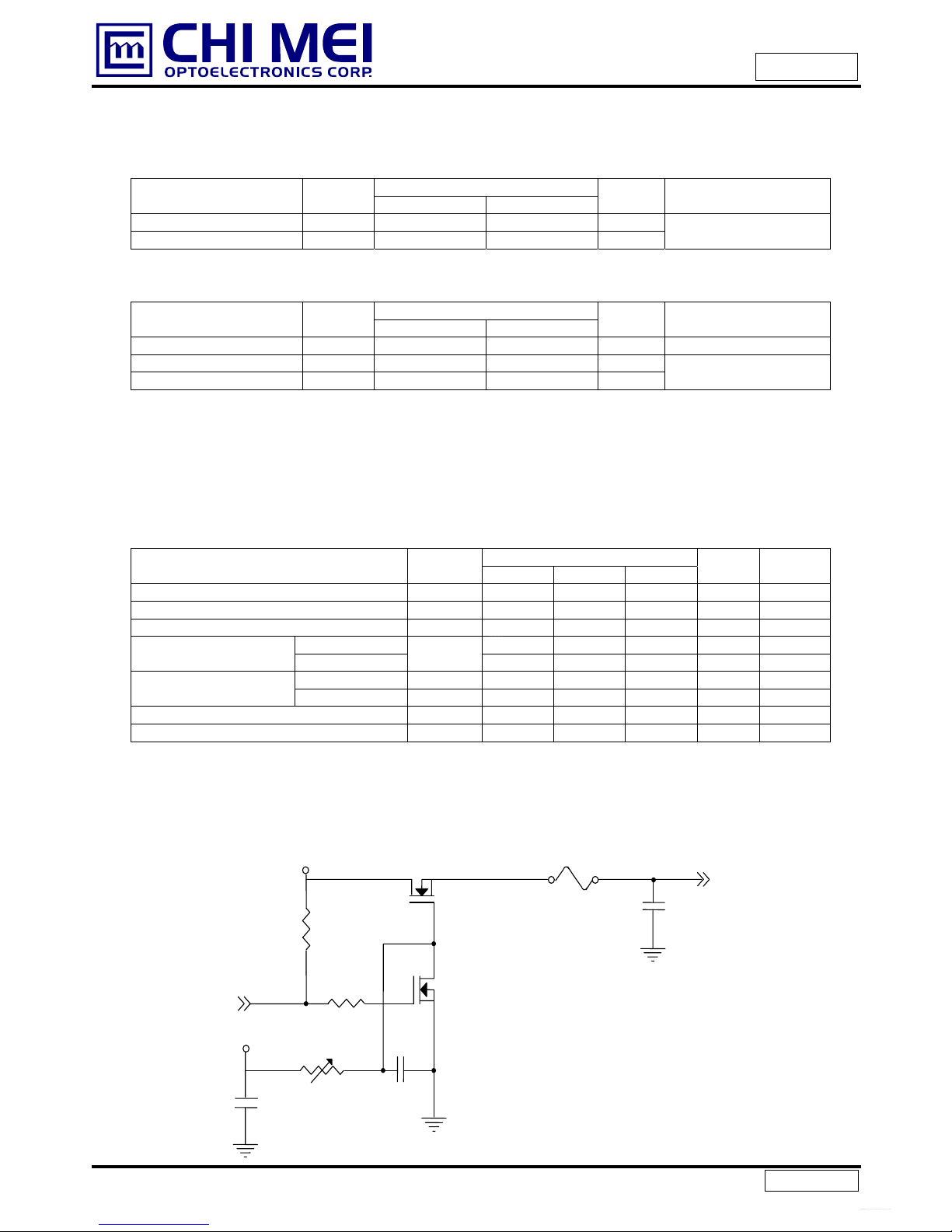
3. ELECTRICAL CHARACTERISTICS
3.1TFTLCDMODULE Ta=25±2ºC
Value
Parameter Symbol Min. Typ. Max.
Unit Note
Power Supply Voltage Vcc 3.0 3.3 3.6 V -
Ripple Voltage VRP - 100 - mV -
Rush Current IRUSH - - 1.5 A (2)
White - 300 350 mA (3)a
Power Supply Current Black Lcc - 350 400 mA (3)b
“H” Level VIL - - +100 mV -Logical Input Voltage
(LVDS) “L” Level VIH -100 - - mV -
Terminating Resistor RT- 100 - Ohm -
Power per EBL WG PEBL - 3.224 - W (4)
Note (1) The module should be always operated within above ranges.
Note (2) Measurement Conditions:
R1
(High to Low)
(Control Signal)
+12V
SW
Q2
C1
1uF
Vcc
+3.3V
2SK1470
Q1 2SK1475
47K
R2
1K
VR1 47K C2
0.01uF
C3
1uF
FUSE (LCD Module Input)
www.DataSheet.net/
Datasheet pdf - http://www.DataSheet4U.co.kr/
Issued Date: Sep.27, 2005
Model No.: N150X3 - L09
Approval
7 / 27
Version 2.2
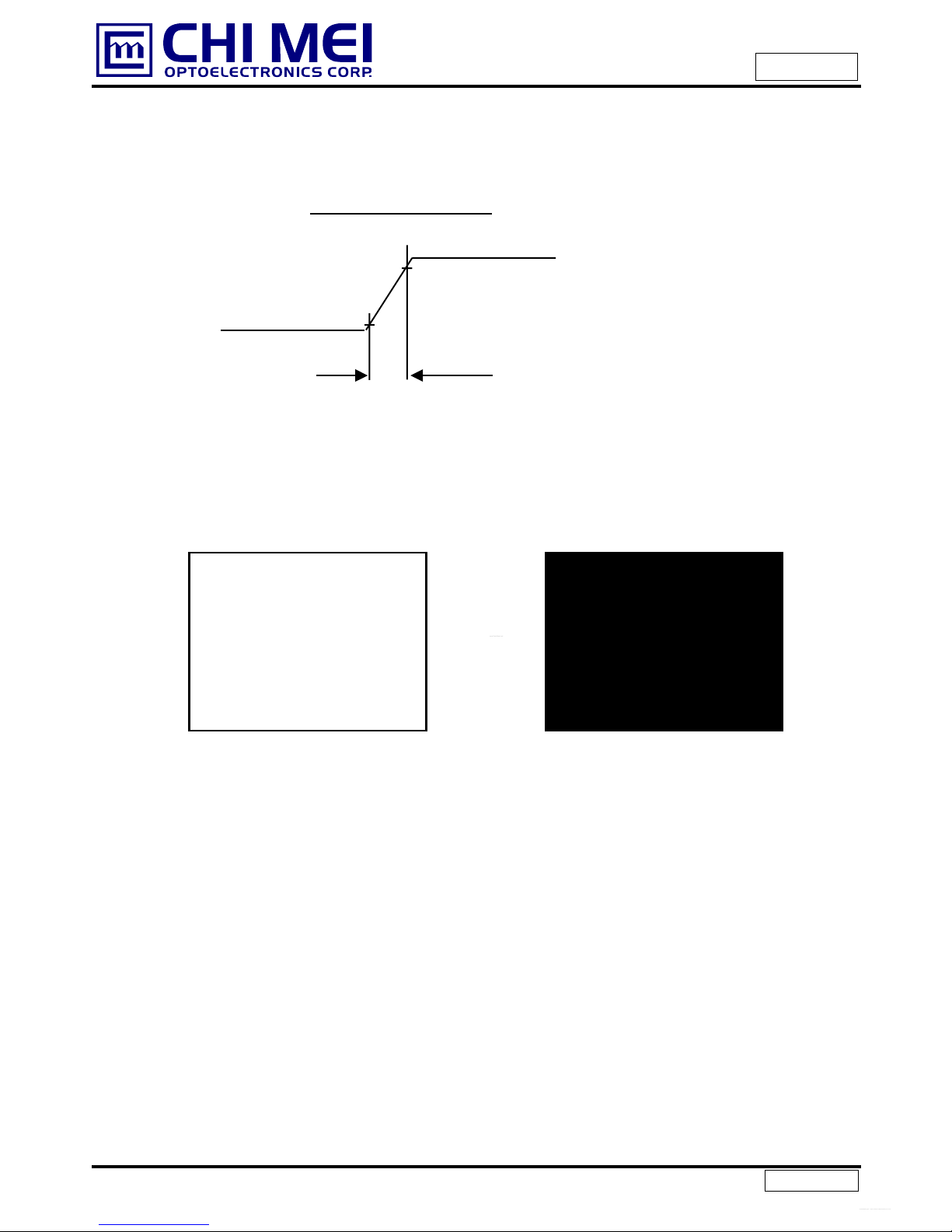
Note (3) The specified power supply current is under the conditions at Vcc = 3.3 V, Ta = 25 ± 2 ºC, fv= 60
Hz, whereas a power dissipation check pattern below is displayed.
Note (4) The specified power are the sum of LCD panel electronics input power and the inverter input
power. Test conditions are as follows.
(a) Vcc = 3.3 V, Ta = 25 ± 2 ºC, fv= 60 Hz,
(b) The pattern used is a black and white 32 x 36 checkerboard, slide #100 from the VESA file
“Flat Panel Display Monitor Setup Patterns”, FPDMSU.ppt.
(c) Luminance: 60 nits.
(d) The inverter used is provided from O2Micro (www.o2micro.com). Please contact O2Mirco for detail
information. CMO doesn’t provide the inverter in this product.
Vcc rising time is 470µs
470µs
+3.3V
GND
0.9Vcc
0.1Vcc
Active Area
a. White Pattern
Active Area
b. Black Pattern
www.DataSheet.net/
Datasheet pdf - http://www.DataSheet4U.co.kr/

Issued Date: Sep.27, 2005
Model No.: N150X3 - L09
Approval
8 / 27
Version 2.2
3.2 BACKLIGHT UNIT Ta=25±2ºC
Value
Parameter Symbol
Min. Typ. Max.
Unit Note
Lamp Input Voltage VL627 660 693 VRMS I
L= 6.0 mA
Lamp Current IL2.0 6.0 6.5 mARMS (1)
--- --- 1165 (25
oC) VRMS (2)
Lamp Turn On Voltage VS--- --- 1400 (0
oC) VRMS (2)
Operating Frequency FL50 --- 80 KHz (3)
Lamp Life Time LBL 15,000 - Hrs (5)
Power Consumption PL- 3.96 - W (4), IL= 6.0 mA
Note (1) Lamp current is measured by utilizing a high frequency current meter as shown below:
Note (2) The voltage shown above should be applied to the lamp for more than 1 second after startup.
Otherwise the lamp may not be turned on.
Note (3) The lamp frequency may produce interference with horizontal synchronous frequency from the
display, and this may cause line flow on the display. In order to avoid interference, the lamp
frequency should be detached from the horizontal synchronous frequency and its harmonics as far
as possible.
Note (4) PL= IL×VL
Note (5) The lifetime of lamp can be defined as the time in which it continues to operate under the condition
Ta = 25 ±2 oC and IL= 6.0 mArms until one of the following events occurs:
(a) When the brightness becomes or lower than 50% of its original value.
(b) When the effective ignition length becomes or lower than 80% of its original value. (Effective
ignition length is defined as an area that has less than 70% brightness compared to the
brightness in the center point.)
Note (6) The waveform of the voltage output of inverter must be area-symmetric and the design of the
inverter must have specifications for the modularized lamp. The performance of the Backlight,
such as lifetime or brightness, is greatly influenced by the characteristics of the DC-AC inverter for
the lamp. All the parameters of an inverter should be carefully designed to avoid producing too
much current leakage from high voltage output of the inverter. When designing or ordering the
inverter please make sure that a poor lighting caused by the mismatch of the Backlight and the
inverter (miss-lighting, flicker, etc.) never occurs. If the above situation is confirmed, the module
should be operated in the same manners when it is installed in your instrument.
LCD
Module
1
Inverter
A
Current Meter
HV (White)
LV (Black) 2
www.DataSheet.net/
Datasheet pdf - http://www.DataSheet4U.co.kr/
Issued Date: Sep.27, 2005
Model No.: N150X3 - L09
Approval
9 / 27
Version 2.2
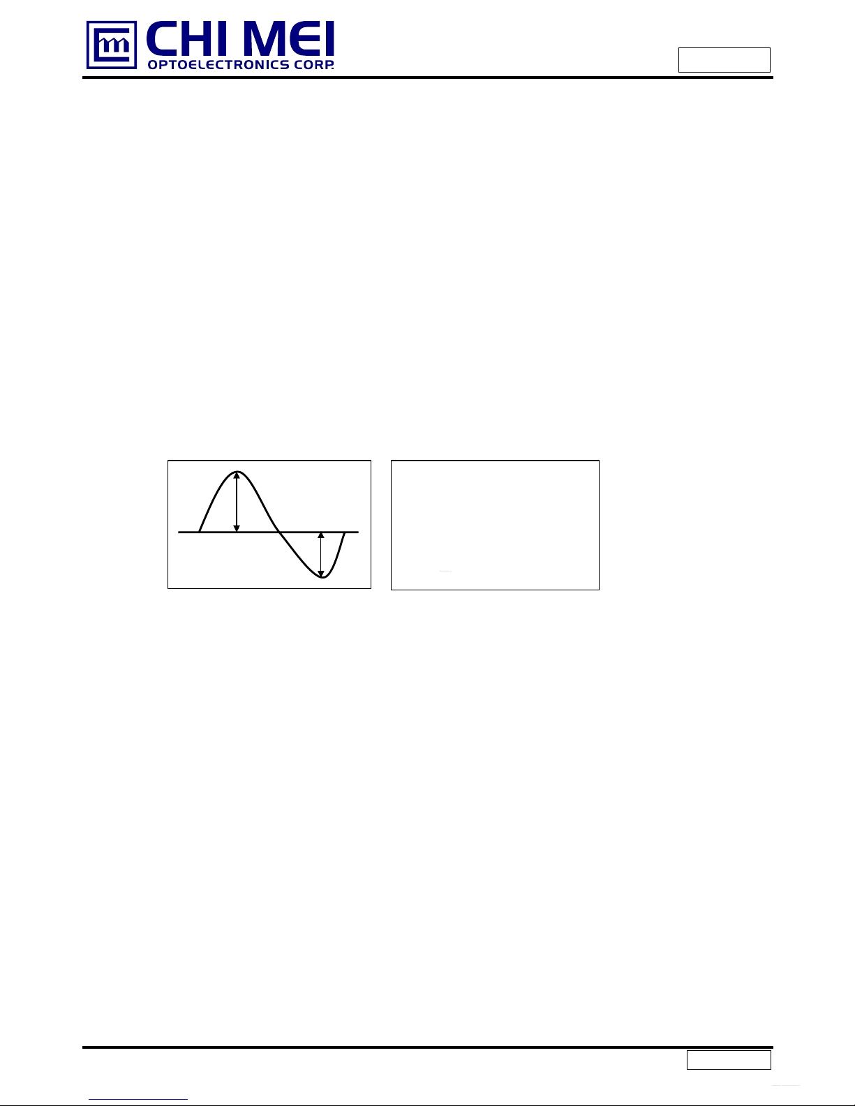
The output of the inverter must have symmetrical (negative and positive) voltage waveform and
symmetrical current waveform.(Unsymmetrical ratio is less than 10%) Please do not use the inverter
which has unsymmetrical voltage and unsymmetrical current and spike wave. Lamp frequency may
produce interface with horizontal synchronous frequency and as a result this may cause beat on the
display. Therefore lamp frequency shall be as away possible from the horizontal synchronous
frequency and from its harmonics in order to prevent interference.
Requirements for a system inverter design, which is intended to have a better display performance, a
better power efficiency and a more reliable lamp. It shall help increase the lamp lifetime and reduce its
leakage current.
a. The asymmetry rate of the inverter waveform should be 10% below;
b. The distortion rate of the waveform should be within √2 ± 10%;
The ideal sine wave form shall be symmetric in positive and negative polarities.
I p
I -p
* Asymmetry rate:
|I
p– I –p | / Irms * 100%
* Distortion rate
I
p(or I –p) / Irms
www.DataSheet.net/
Datasheet pdf - http://www.DataSheet4U.co.kr/
Issued Date: Sep.27, 2005
Model No.: N150X3 - L09
Approval
10 / 27
Version 2.2
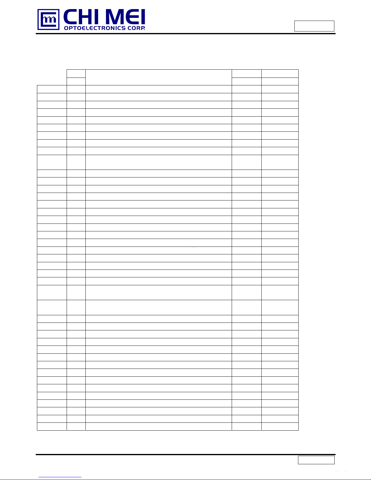
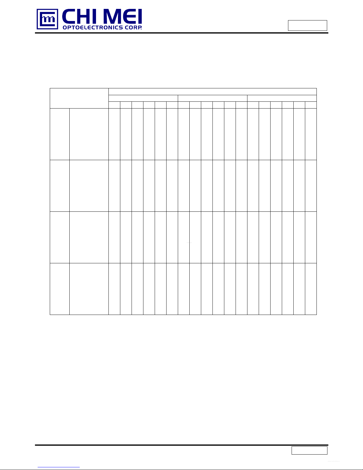
3.3 EDID DATA
The following data is based on VESA Enhanced EDID proposal.
Byte # Byte Value Value
(decimal) (hex) Field Name and Comments (hex) (binary)
0 0 Header 00 00000000
1 1 Header FF 11111111
2 2 Header FF 11111111
3 3 Header FF 11111111
4 4 Header FF 11111111
5 5 Header FF 11111111
6 6 Header FF 11111111
7 7 Header 00 00000000
8 8 EISA ID manufacturer name (“CMO”) 0D 00001101
9 9 EISA ID manufacturer name (Compressed ASCII) AF 10101111
10 0A ID product code 13 00010011
11 0B ID product code 15 00010101
12 0C ID S/N (fixed “0”) 00 00000000
13 0D ID S/N (fixed “0”) 00 00000000
14 0E ID S/N (fixed “0”) 00 00000000
15 0F ID S/N (fixed “0”) 00 00000000
16 10 Week of manufacture (fixed week code) 00 00000000
17 11 Year of manufacture (fixed year code) 00 00000000
18 12 EDID structure version # (“1”) 01 00000001
19 13 EDID revision # (“3”) 03 00000011
20 14 Video I/P definition (“digital”) 80 10000000
21 15 Max H image size (“30.4128 cm”) 1E 00011110
22 16 Max V image size (“22.8096 cm”) 17 00010111
23 17 Display Gamma (Gamma = ”2.2”) 78 01111000
24 18 Feature support (“Active off, RGB Color”) 0A 00001010
25 19 Red/Green (Rx1, Rx0, Ry1, Ry0, Gx1, Gx0, Gy1, Gy0) 77 01110111
26 1A Blue/White (Bx1, Bx0, By1, By0, Wx1, Wx0, Wy1, Wy0) F1 11110001
27 1B Red-x (Rx = “0.626”) A0 10100000
28 1C Red-y (Ry = “0.355”) 5A 01011010
29 1D Green-x (Gx = ”0.294”) 4B 01001011
30 1E Green-y (Gy = ”0.589”) 96 10010110
31 1F Blue-x (Bx = ”0.144”) 24 00100100
32 20 Blue-y (By = ”0.097”) 18 00011000
33 21 White-x (Wx = ”0.309”) 4F 01001111
34 22 White-y (Wy = ”0.329”) 54 01010100
35 23 Established timings 1 00 00000000
36 24 Established timings 2 08 00001000
37 25 Manufacturer’s reserved timings 00 00000000
38 26 Standard timing ID # 1 01 00000001
39 27 Standard timing ID # 1 01 00000001
40 28 Standard timing ID # 2 01 00000001
41 29 Standard timing ID # 2 01 00000001
www.DataSheet.net/
Datasheet pdf - http://www.DataSheet4U.co.kr/

Issued Date: Sep.27, 2005
Model No.: N150X3 - L09
Approval
11 / 27
Version 2.2
42 2A Standard timing ID # 3 01 00000001
43 2B Standard timing ID # 3 01 00000001
44 2C Standard timing ID # 4 01 00000001
45 2D Standard timing ID # 4 01 00000001
46 2E Standard timing ID # 5 01 00000001
47 2F Standard timing ID # 5 01 00000001
48 30 Standard timing ID # 6 01 00000001
49 31 Standard timing ID # 6 01 00000001
50 32 Standard timing ID # 7 01 00000001
51 33 Standard timing ID # 7 01 00000001
52 34 Standard timing ID # 8 01 00000001
53 35 Standard timing ID # 8 01 00000001
54 36 Detailed timing description # 1 Pixel clock (“65 MHz”) 64 01100100
55 37 # 1 Pixel clock (hex LSB first) 19 00011001
56 38 # 1 H active (“1024”) 00 00000000
57 39 # 1 H blank (“320”) 40 01000000
58 3A # 1 H active : H blank (“1024 : 320”) 41 01000001
59 3B # 1 V active (”768”) 00 00000000
60 3C # 1 V blank (”38”) 26 00100110
61 3D # 1 V active : V blank (”768 : 38”) 30 00110000
62 3E # 1 H sync offset (”24”) 18 00011000
63 3F # 1 H sync pulse width (”136”) 88 10001000
64 40 # 1 V sync offset : V sync pulse width (”3 : 6”) 36 00110110
65 41
# 1 H sync offset : H sync pulse width : V sync offset : V
sync width (”24 : 136 : 3 : 6”) 00 00000000
66 42 # 1 H image size (”304.128 mm”) 30 00110000
67 43 # 1 V image size (”228.096 mm”) E4 11100100
68 44 # 1 H image size : V image size (”304 : 228”) 10 00010000
69 45 # 1 H boarder (”0”) 00 00000000
70 46 # 1 V boarder (”0”) 00 00000000
71 47
# 1 Non-interlaced, Normal, no stereo, Separate sync,
H/V pol Negatives 18 00011000
72 48 Detailed timing description # 2 00 00000000
73 49 # 2 Flag 00 00000000
74 4A # 2 Reserved 00 00000000
75 4B
# 2 FE (hex) defines ASCII string (Model Name
“N150X3-L09”, ASCII) FE 11111110
76 4C # 2 Flag 00 00000000
77 4D # 2 1st character of name (“N”) 4E 01001110
78 4E # 2 2nd character of name (“1”) 31 00110001
79 4F # 2 3rd character of name (“5”) 35 00110101
80 50 # 2 4th character of name (“0”) 30 00110000
81 51 # 2 5th character of name (“X”) 58 01011000
82 52 # 2 6th character of name (“3”) 33 00110011
83 53 # 2 7th character of name (“-”) 2D 00101101
84 54 # 2 8th character of name (“L”) 4C 01001100
85 55 # 2 9th character of name (“0”) 30 00110000
86 56 # 2 10th character of name (“9”) 39 00111001
www.DataSheet.net/
Datasheet pdf - http://www.DataSheet4U.co.kr/
Issued Date: Sep.27, 2005
Model No.: N150X3 - L09
Approval
12 / 27
Version 2.2
87 57
(If <13 char, then terminate with ASCII code 0Ah, set
remaining char = 20h) 0A 00001010
88 58
(If <13 char, then terminate with ASCII code 0Ah, set
remaining char = 20h) 20 00100000
89 59
(If <13 char, then terminate with ASCII code 0Ah, set
remaining char = 20h) 20 00100000
90 5A Detailed timing description # 3 00 00000000
91 5B # 3 Flag 00 00000000
92 5C # 3 Reserved 00 00000000
93 5D # 3 FE (hex) defines ASCII string (Vendor “CMO”, ASCII) FE 11111110
94 5E # 3 Flag 00 00000000
95 5F # 3 1st character of string (“C”) 43 01000011
96 60 # 3 2nd character of string (“M”) 4D 01001101
97 61 # 3 3rd character of string (“O”) 4F 01001111
98 62
(If <13 char, then terminate with ASCII code 0Ah, set
remaining char = 20h) 0A 00001010
99 63
(If <13 char, then terminate with ASCII code 0Ah, set
remaining char = 20h) 20 00100000
100 64
(If <13 char, then terminate with ASCII code 0Ah, set
remaining char = 20h) 20 00100000
101 65
(If <13 char, then terminate with ASCII code 0Ah, set
remaining char = 20h) 20 00100000
102 66
(If <13 char, then terminate with ASCII code 0Ah, set
remaining char = 20h) 20 00100000
103 67
(If <13 char, then terminate with ASCII code 0Ah, set
remaining char = 20h) 20 00100000
104 68
(If <13 char, then terminate with ASCII code 0Ah, set
remaining char = 20h) 20 00100000
105 69
(If <13 char, then terminate with ASCII code 0Ah, set
remaining char = 20h) 20 00100000
106 6A
(If <13 char, then terminate with ASCII code 0Ah, set
remaining char = 20h) 20 00100000
107 6B
(If <13 char, then terminate with ASCII code 0Ah, set
remaining char = 20h) 20 00100000
108 6C Detailed timing description # 4 00 00000000
109 6D # 4 Flag 00 00000000
110 6E # 4 Reserved 00 00000000
111 6F
# 4 FE (hex) defines ASCII string (Model
Name“N150X3-L09”, ASCII) FE 11111110
112 70 # 4 Flag 00 00000000
113 71 # 4 1st character of name (“N”) 4E 01001110
114 72 # 4 2nd character of name (“1”) 31 00110001
115 73 # 4 3rd character of name (“5”) 35 00110101
116 74 # 4 4th character of name (“0”) 30 00110000
117 75 # 4 5th character of name (“X”) 58 01011000
118 76 # 4 6th character of name (“3”) 33 00110011
119 77 # 4 7th character of name (“-”) 2D 00101101
120 78 # 4 8th character of name (“L”) 4C 01001100
121 79 # 4 9th character of name (“0”) 30 00110000
122 7A # 4 10th character of name (“9”) 39 00111001
123 7B
(If <13 char, then terminate with ASCII code 0Ah, set
remaining char = 20h) 0A 00001010
www.DataSheet.net/
Datasheet pdf - http://www.DataSheet4U.co.kr/
Issued Date: Sep.27, 2005
Model No.: N150X3 - L09
Approval
13 / 27
Version 2.2
124 7C
(If <13 char, then terminate with ASCII code 0Ah, set
remaining char = 20h) 20 00100000
125 7D
(If <13 char, then terminate with ASCII code 0Ah, set
remaining char = 20h) 20 00100000
126 7E Extension flag 00 00000000
127 7F Checksum 0E 00001110
www.DataSheet.net/
Datasheet pdf - http://www.DataSheet4U.co.kr/

Issued Date: Sep.27, 2005
Model No.: N150X3 - L09
Approval
14 / 27
Version 2.2
4. BLOCK DIAGRAM
4.1 TFT LCD MODULE
4.2 BACKLIGHT UNIT
5. INPUT TERMINAL PIN ASSIGNMENT
5.1 TFT LCD MODULE
Pin Symbol Description Polarity Remark
1 Vss Ground
2 Vcc Power Supply +3.3 V (typical)
3 Vcc Power Supply +3.3 V (typical)
4 VEDID DDC 3.3V Power DDC 3.3V Power
5 NC Non-Connection
6 CLKEDID DDC Clock DDC Clock
7 DATAEDID DDC Data DDC Data
8 Rxin0- LVDS Differential Data Input Negative
9 Rxin0+ LVDS Differential Data Input Positive
R0~R5,G0
-
10 Vss Ground
11 Rxin1- LVDS Differential Data Input Negative G1~G5,B0,B1
VEDID
DataEDID
Vcc
GND
VL
CLK(+/-)
Rxin2(+/-)
Rxin1(+/-)
Rxin0(+/-)
TFT LCD PANEL
(1024xR.G.B.x768)
DATA DRIVER IC
SCAN DRIVER IC
BACKLIGHT UNIT
LVDS INPUT /
TIMING CONTROLLER
DC/DC CONVERTER &
REFERENCE VOLTAGE
GENERATOR
INPUT CONNECTOR
(JAE-FI-XB30S-HF10)
LAMP CONNECTOR
(JST-BHSR-02VS-1)
EDID
EEPROM
CLKEDID
1 HV (White)
2 LV
(
Black
)
www.DataSheet.net/
Datasheet pdf - http://www.DataSheet4U.co.kr/

Issued Date: Sep.27, 2005
Model No.: N150X3 - L09
Approval
15 / 27
Version 2.2
12 Rxin1+ LVDS Differential Data Input Positive
-
13 Vss Ground
14 Rxin2- LVDS Differential Data Input Negative
15 Rxin2+ LVDS Differential Data Input Positive
B2~B5,DE,Hsync,Vsync
16 Vss Ground
17 CLK- LVDS Clock Data Input Negative
18 CLK+ LVDS Clock Data Input Positive LVDS Level Clock
19 Vss Ground
20 NC Non-Connection
21 NC Non-Connection
22 Vss Ground
23 NC Non-Connection
24 NC Non-Connection
25 Vss Ground
26 NC Non-Connection
27 NC Non-Connection
28 Vss Ground
29 NC Non-Connection
30 NC Non-Connection
Note (1) Connector Part No.: JAE-FI-XB30SL-HF10 or equivalent
Note (2) User’s connector Part No: JAE-FI-X30C2L or equivalent
Note (3) The first pixel is even.
5.2 TIMING DIAGRAM OF LVDS INPUT SIGNAL
IN6 IN5 IN4 IN3 IN2 IN1 IN0
IN13 IN12 IN11 IN10 IN9 IN8 IN7
IN20 IN19 IN18 IN17 IN16 IN15 IN14
G0 R3 R2 R1 R0R5 R4
B1 G4 G3 G2 G1B0 G5
DE B5 B4 B3 B2Vsync Hsync
T/7
Signal for 1 DCLK Cycle (T)
Rxin0
Rxin1
Rxin2
CLK+
www.DataSheet.net/
Datasheet pdf - http://www.DataSheet4U.co.kr/
Issued Date: Sep.27, 2005
Model No.: N150X3 - L09
Approval
16 / 27
Version 2.2
5.3 COLOR DATA INPUT ASSIGNMENT
The brightness of each primary color (red, green and blue) is based on the 6-bit gray scale data input for
the color. The higher the binary input, the brighter the color. The table below provides the assignment of
color versus data input.
Data Signal
Red Green Blue
Color
R5 R4 R3 R2 R1 R0 G5 G4 G3 G2 G1 G0 B5 B4 B3 B2 B1 B0
Basic
Colors
Black
Red
Green
Blue
Cyan
Magenta
Yellow
White
0
1
0
0
0
1
1
1
0
1
0
0
0
1
1
1
0
1
0
0
0
1
1
1
0
1
0
0
0
1
1
1
0
1
0
0
0
1
1
1
0
1
0
0
0
1
1
1
0
0
1
0
1
0
1
1
0
0
1
0
1
0
1
1
0
0
1
0
1
0
1
1
0
0
1
0
1
0
1
1
0
0
1
0
1
0
1
1
0
0
1
0
1
0
1
1
0
0
0
1
1
1
0
1
0
0
0
1
1
1
0
1
0
0
0
1
1
1
0
1
0
0
0
1
1
1
0
1
0
0
0
1
1
1
0
1
0
0
0
1
1
1
0
1
Gray
Scale
Of
Red
Red(0)/Dark
Red(1)
Red(2)
:
:
Red(61)
Red(62)
Red(63)
0
0
0
:
:
1
1
1
0
0
0
:
:
1
1
1
0
0
0
:
:
1
1
1
0
0
0
:
:
1
1
1
0
0
1
:
:
0
1
1
0
1
0
:
:
1
0
1
0
0
0
:
:
0
0
0
0
0
0
:
:
0
0
0
0
0
0
:
:
0
0
0
0
0
0
:
:
0
0
0
0
0
0
:
:
0
0
0
0
0
0
:
:
0
0
0
0
0
0
:
:
0
0
0
0
0
0
:
:
0
0
0
0
0
0
:
:
0
0
0
0
0
0
:
:
0
0
0
0
0
0
:
:
0
0
0
0
0
0
:
:
0
0
0
Gray
Scale
Of
Green
Green(0)/Dark
Green(1)
Green(2)
:
:
Green(61)
Green(62)
Green(63)
0
0
0
:
:
0
0
0
0
0
0
:
:
0
0
0
0
0
0
:
:
0
0
0
0
0
0
:
:
0
0
0
0
0
0
:
:
0
0
0
0
0
0
:
:
0
0
0
0
0
0
:
:
1
1
1
0
0
0
:
:
1
1
1
0
0
0
:
:
1
1
1
0
0
0
:
:
1
1
1
0
0
1
:
:
0
1
1
0
1
0
:
:
1
0
1
0
0
0
:
:
0
0
0
0
0
0
:
:
0
0
0
0
0
0
:
:
0
0
0
0
0
0
:
:
0
0
0
0
0
0
:
:
0
0
0
0
0
0
:
:
0
0
0
Gray
Scale
Of
Blue
Blue(0)/Dark
Blue(1)
Blue(2)
:
:
Blue(61)
Blue(62)
Blue(63)
0
0
0
:
:
0
0
0
0
0
0
:
:
0
0
0
0
0
0
:
:
0
0
0
0
0
0
:
:
0
0
0
0
0
0
:
:
0
0
0
0
0
0
:
:
0
0
0
0
0
0
:
:
0
0
0
0
0
0
:
:
0
0
0
0
0
0
:
:
0
0
0
0
0
0
:
:
0
0
0
0
0
0
:
:
0
0
0
0
0
0
:
:
0
0
0
0
0
0
:
:
1
1
1
0
0
0
:
:
1
1
1
0
0
0
:
:
1
1
1
0
0
0
:
:
1
1
1
0
0
1
:
:
0
1
1
0
1
0
:
:
1
0
1
Note (1) 0: Low Level Voltage, 1: High Level Voltage
www.DataSheet.net/
Datasheet pdf - http://www.DataSheet4U.co.kr/
Issued Date: Sep.27, 2005
Model No.: N150X3 - L09
Approval
17 / 27
Version 2.2
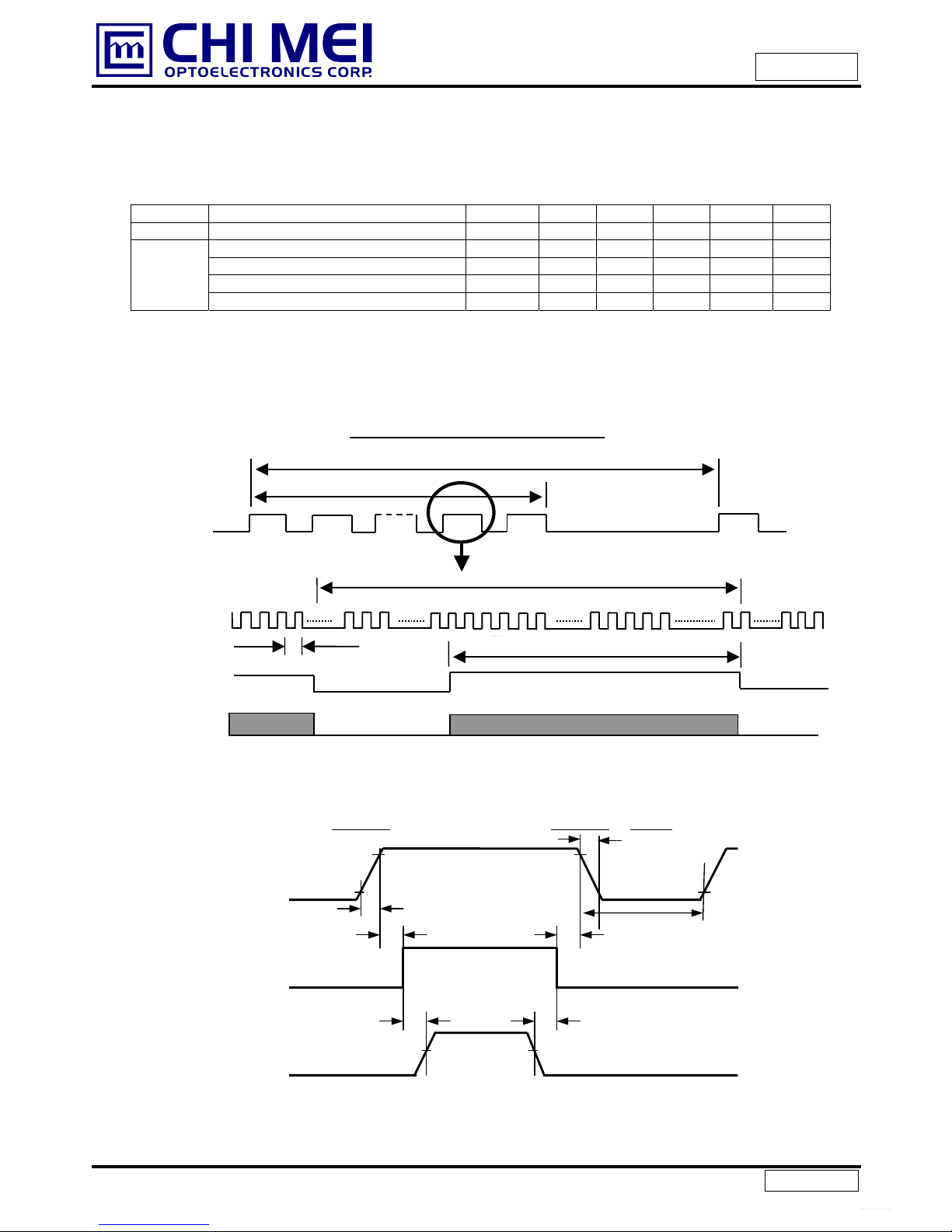
6. INTERFACE TIMING
6.1 INPUT SIGNAL TIMING SPECIFICATIONS
The input signal timing specifications are shown as the following table and timing diagram.
Signal Item Symbol Min. Typ. Max. Unit Note
DCLK Frequency 1/Tc 50 65 68 MHz -
Frame Time Cycle TV 771 806 850 TH -
Vertical Active Display Period TVD 768 768 768 TH -
One Line Scanning Time Cycle TH 1200 1344 1600 Tc -
DE
Horizontal Active Display Period THD 1024 1024 1024 Tc -
Note (1) Because this module is operated by DE only mode, Hsync and Vsync input signals should be set
to low logic level or ground. Otherwise, this module would operate abnormally.
INPUT SIGNAL TIMING DIAGRAM
6.2 POWER ON/OFF SEQUENCE
-
Power Supply
for LCD, Vcc
- Interface Signal
(LVDS Signal of
Transmitter), VI
-Power for Lamp
Restart
Power On Power Off
50%50%
0V
0V
10%
t6t5
t4
t3t2
t1
90%
10%
90%
Valid Data
ONOFF OFF
T
H
TC
DCLK
THD
T
VD
T
v
DE
DE
DATA
t7
10%
www.DataSheet.net/
Datasheet pdf - http://www.DataSheet4U.co.kr/

Issued Date: Sep.27, 2005
Model No.: N150X3 - L09
Approval
18 / 27
Version 2.2
Timing Specifications:
0.47 < t1 ≦10 msec
0 < t2 ≦50 msec
0 < t3 ≦50 msec
t4 ≧500 msec
t5 ≧200 msec
t6 ≧200 msec
Note (1) Please avoid floating state of interface signal at invalid period.
Note (2) When the interface signal is invalid, be sure to pull down the power supply of LCD Vcc to 0 V.
Note (3) The Backlight inverter power must be turned on after the power supply for the logic and the
interface signal is valid. The Backlight inverter power must be turned off before the power supply
for the logic and the interface signal is invalid.
Note (4) Sometimes some slight noise shows when LCD is turned off (even backlight is already off). To
avoid this phenomenon, we suggest that the Vcc falling time had better to follow
t7 ≧5 msec
www.DataSheet.net/
Datasheet pdf - http://www.DataSheet4U.co.kr/
Table of contents
Other Chimei Monitor manuals


Popular Monitor manuals by other brands


Dell
Dell S2719DM user guide

Daktronics
Daktronics Galaxy Series DISPLAY MANUAL

Siebert
Siebert Series S102 operating instructions

IEE
IEE 03858-21-0105 reference guide

TSI Instruments
TSI Instruments PRESSURA RPM10 Installation instructions and safety information

Sun Microsystems
Sun Microsystems GDM-5510 Quick setup guide


