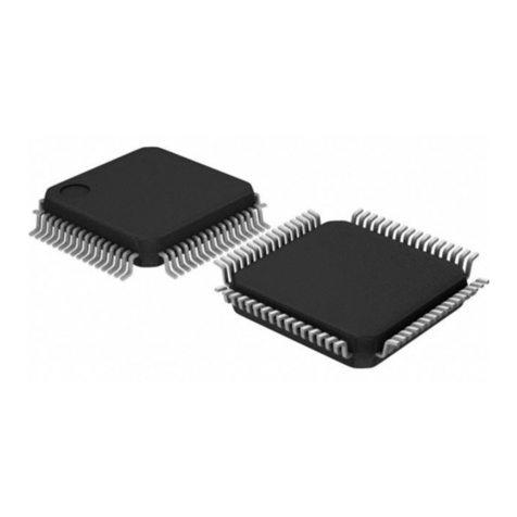
Cirrus Logic Crystal LAN CS8900A User manual

1
Copyright Cirrus Logic, Inc. 2001
(All Rights Reserved)
Cirrus Logic, Inc.
P.O. Box 17847, Austin, Texas 78760
(512) 445 7222 FAX: (512) 445 7581
http://www.cirrus.com
AN83
Application Note
&U\VWDO/$1 CS8900A ETHERNET CONTROLLER
TECHNICAL REFERENCE MANUAL
By Deva Bodas
Revised by James Ayres
JUN ‘01
AN83REV3

AN83
2AN83REV3
TABLE OF CONTENTS
SCHEMATIC CHECKLIST ...................................................................................................................................4
SOFTWARE CHECKLIST ....................................................................................................................................5
INTRODUCTION TO CS8900A TECHNICAL REFERENCE MANUAL ..............................................................6
HARDWARE DESIGN ..........................................................................................................................................7
CS8900A: CONNECTING TO NON-ISA BUS SYSTEMS ...................................................................................7
The CS8900A Architecture.............................................................................................................................7
ISA Bus ....................................................................................................................................................8
CS8900A in I/O Mode ..............................................................................................................................8
CS8900A in Memory Mode......................................................................................................................8
DMA Interface of the CS8900A................................................................................................................8
Selection of I/O, Memory and DMA Modes ....................................................................................................9
Design Example: CS8900A Interface to MC68302 ........................................................................................9
Address Generation .................................................................................................................................9
Read and Write Signals .........................................................................................................................10
SBHE Signal ..........................................................................................................................................10
Other Control Signals.............................................................................................................................10
Status Signals from CS8900A ...............................................................................................................11
Databus (SD[0:15]) Connection....................................................................................................................11
Checklist for Signal Connections to the CS8900A .......................................................................................11
EEPROM Optional........................................................................................................................................11
Design Example: CS8900A Interface to Cirrus Logic CL-PS7111 ...............................................................12
Design Example: CS8900A Interface to Hitachi SH3 ...................................................................................12
Summary ......................................................................................................................................................12
ETHERNET HARDWARE DESIGN FOR EMBEDDED SYSTEMS AND MOTHERBOARDS ..........................15
General Description ...............................................................................................................................15
Board Design Considerations ................................................................................................................15
Crystal Oscillator .............................................................................................................................15
ISA Bus Interface ............................................................................................................................15
External Decode Logic ....................................................................................................................15
EEPROM.........................................................................................................................................15
LEDs................................................................................................................................................18
10BASE-T Interface ........................................................................................................................18
10BASE-2 and AUI Interfaces.........................................................................................................18
Logic Schematics...................................................................................................................................18
Component Placement and Signal Routing ........................................................................................20
Bill of Material ........................................................................................................................................20
Contacting Cirrus Logic Support
For a complete listing of Direct Sales, Distributor, and Sales Representative contacts, visit the Cirrus Logic web site at:
http://www.cirrus.com/corporate/contacts/
Crystal LAN, StreamTransfer, PacketPage, and SMART Analog are trademarks of Cirrus Logic.
Ethernet is a registered trademark of Xerox Corp.. Artisoft and LANtastic are registered trademarks of Artisoft, Inc.. Banyan and VINES are registered trademarks
of Banyan Systems.. Digital and PATHWORKS are registered trademarks of Digital Equipment Corporation.. Intel is a registered trademark of Intel Corporation..
LAN Server and IBM are registered trademarks of International Business Machines Corp.. Microsoft, LAN Manager, Windows 95, Windows for Workgroups, and
Windows NT are registered trademarks of Microsoft.. Novell and Netware are registered trademarks of Novell, Inc..
SCO is a registered trademark of Santa
Cruz Organization, Inc
.. UNIX is a registered trademark of AT&T Technologies, Inc.
Preliminary product information describes products which are in production, but for which full characterization data is not yet available. Advance product infor-
mation describes products which are in development and subject to development changes. Cirrus Logic, Inc. has made best efforts to ensure that the information
contained in this document is accurate and reliable. However, the information is subject to change without notice and is provided “AS IS” without warranty of
any kind (express or implied). No responsibility is assumed by Cirrus Logic, Inc. for the use of this information, nor for infringements of patents or other rights
of third parties. This document is the property of Cirrus Logic, Inc. and implies no license under patents, copyrights, trademarks, or trade secrets. No part of
this publication may be copied, reproduced, stored in a retrieval system, or transmitted, in any form or by any means (electronic, mechanical, photographic, or
otherwise) without the prior written consent of Cirrus Logic, Inc. Items from any Cirrus Logic website or disk may be printed for use by the user. However, no
part of the printout or electronic files may be copied, reproduced, stored in a retrieval system, or transmitted, in any form or by any means (electronic, mechanical,
photographic, or otherwise) without the prior written consent of Cirrus Logic, Inc.Furthermore, no part of this publication may be used as a basis for manufacture
or sale of any items without the prior written consent of Cirrus Logic, Inc. The names of products of Cirrus Logic, Inc. or other vendors and suppliers appearing
in this document may be trademarks or service marks of their respective owners which may be registered in some jurisdictions. A list of Cirrus Logic, Inc. trade-
marks and service marks can be found at http://www.cirrus.com.

AN83
AN83REV3 3
LOW COST ETHERNET COMBO CARD REFERENCE DESIGN: CRD8900 ..................................................21
General Description ...............................................................................................................................21
Board Design .........................................................................................................................................21
Crystal Oscillator .............................................................................................................................21
ISA Bus Interface ............................................................................................................................21
External Decode Logic ....................................................................................................................21
EEPROM.........................................................................................................................................21
Socket for Optional Boot PROM .....................................................................................................21
LEDs ...............................................................................................................................................26
10BASE-T Interface ........................................................................................................................26
AUI Interface ...................................................................................................................................26
10BASE-2 Interface ........................................................................................................................27
Logic Schematics...................................................................................................................................27
Component Placement and Routing of Signals .....................................................................................27
Bill of Material ........................................................................................................................................27
Addressing the CS8900A: I/O Mode, Memory Mode ...................................................................................27
I/O Mode................................................................................................................................................27
Memory Mode........................................................................................................................................31
Lower Memory Mode ......................................................................................................................31
Extended Memory Mode .................................................................................................................31
Layout Considerations for the CS8900A......................................................................................................35
General Guidelines ................................................................................................................................35
Power Supply Connections....................................................................................................................35
Two Layered Printed Circuit Board (PCB) ......................................................................................35
Multi-layered Printed Circuit Board .................................................................................................35
Routing of the Digital Signals.................................................................................................................35
Routing of the Analog Signals ...............................................................................................................35
RECOMMENDED MAGNETICS FOR THE CS8900A .......................................................................................44
JUMPERLESS DESIGN.....................................................................................................................................45
Serial EEPROM............................................................................................................................................45
Reset Configuration Block .....................................................................................................................45
Driver Configuration Information............................................................................................................47
Format of Driver Configuration Block.....................................................................................................47
IEEE Physical Address ...................................................................................................................49
ISA Configuration Flags ..................................................................................................................49
PacketPage Memory Base..............................................................................................................50
Boot PROM Memory Base.............................................................................................................50
Boot PROM Mask ..........................................................................................................................50
Transmission Control ......................................................................................................................50
Adapter Configuration Word............................................................................................................51
EEPROM Revision..........................................................................................................................51
Manufacturing Date.........................................................................................................................52
IEEE Physical Address (Copy)........................................................................................................52
16-bit Checksum .............................................................................................................................52
EISA ID ...........................................................................................................................................52
Serial Number .................................................................................................................................53
Serial ID Checksum ........................................................................................................................53
Maintaining EEPROM Information.........................................................................................................54
Embedded Designs......................................................................................................................................54
BIOS-Based Design Considerations......................................................................................................54
Driver Interface with BIOS-Based Configuration ...................................................................................54
OBTAINING IEEE ADDRESSES ....................................................................................................................... 55
DEVICE DRIVERS AND SETUP/INSTALLATION SOFTWARE.......................................................................56
DOS Setup and Installation Utility ................................................................................................................56
Installation Procedure ............................................................................................................................56
CONTACTING CUSTOMER SUPPORT AT CIRRUS .......................................................................................57
Cirrus Web Site ............................................................................................................................................57

AN83
4AN83REV3
SCHEMATIC CHECKLIST
Before getting into the meat of the technical refer-
ence manual here is a schematic checklist. It’s pre-
sented here, at the beginning, to help the hardware
designer implement the design quickly and easily.
-No caps across the crystal. The CS8900A
implements these internally.
-4.99K 1% resistor between pin 93 and pin 94. A
common mistake is the resistor is connected to
Vcc instead of ground.
-RESET is active high, not active low.
-Check addressing.
-On non-ISA systems, if the processor is Big
Endian, it may be beneficial to byte swap the
data lines to minimize byte swapping in
software.
-SBHE (16 bit mode) -- must be low on IO or Mem
address. And it must toggle at least once to put
the CS8900 in 16 bit mode.
-IO and Memory Accesses: SBHE, AEN, etc.
must be stable for 10ns (read) and 20ns (write)
before access.
-IOCHRDY - Generally not connected in non-ISA
bus.
-CHIPSEL (active low). Tie to ground if not using
ELCS.
-Make sure interrupt line is active high. It is best
to put a pull down (10K) on INT line since
selected IRQ line is tristated during software
initiated reset.
-ELCS should be pulled to ground or left floating
if not used.
-EEDataIn should be pulled to ground if not used.
-10Base-T circuit -- no caps on TX lines between
isolation transformer and 10 Base-T connector.
-10Base-T circuit -- no center tap caps on
isolation transformer and 10 Base-T connector.
Good to have pads, don’t populate except for
EMI problems.
-Isolation transformer -- start with one that does
not have a common mode choke. If there are
EMI considerations, then use one with common
mode choke. The pin outs are the same. For
3.3V operation, use a transformer with 1:2.5
turns ration on TX and 1:1 on RX like the Halo
TG41-2006N.
-For EMI problems, 1) add choke, 2) add center
tap caps on isolation transformer
-If using a shielded RJ45 connector, make sure
the shield pins are connected to chassis ground.
-AEN connected to ground if not using DMA.
-AEN can be used as an active low chip select if
not using DMA.
-AUI Interface -- use a 1AMP fuse. MAU can use
.5amps even better use a thermistor ("poly
switch"). Also, use a diode so can’t back-drive
from an externally powered MAU. Use a Halo
TnT integrated module to simplify 10Base2
interface.
-TX series termination resistors are R: 24.3 Ohm
1% (8 or 8.2 Ohm 1% for 3.3V)
-RX shunt termination resistor is 100 Ohm
-Put a 68pF shunt across TX on primary side
(560pF for 3.3V)
-Don’t use split analog/digital power and ground
planes.
-Void ground/power plane from transformer to
RJ45
-Put .1uF cap on each supply pin very close to
CS8900
The schematic checklist and the example connec-
tion diagrams to the Hitachi SH3, Cirrus Logic CL-
PS7211 and the Motorola MC68302 microproces-
sors should make clear the necessary the hardware
connections for a wide variety of situations.

AN83
AN83REV3 5
SOFTWARE CHECKLIST
-When servicing the interrupt always read the
Interrupt Status Queue (ISQ) first. Process that
individual event before reading the ISQ again.
-Having read an ISQ event indicating a valid
recieve frame, never read the ISQ again before
either 1) reading in the entire current receive
frame or 2) issuing an explicit skip command.
Either of these actions will correctly clear that
frame from the CS8900A’s internal memory.
-Always continue reading and processing ISQ
events until reading a 0x0000 from the ISQ.
-After a software or hardware reset, always wait
until the SelfStatus register, bit 7 (INITD) is set
before reading or writing any other registers.
-Allow only one transmit in progress at any given
time. Since the chip dynamically allocates
memory between transmit and recieve frames, it
is possible to fill the internal buffers with transmit
frames. This would prevent reception.
-Don’t reinvent the wheel. Port one of the sample
drivers, if there isn’t a driver for your operating
system. You can find sample drivers at
http://www.cirrus.com/drivers/ethernet/.
AN83
6AN83REV3
INTRODUCTION TO CS8900A
TECHNICAL REFERENCE MANUAL
This Technical Reference Manual provides the in-
formation which will be helpful in designing a
board using the CS8900A, programming the asso-
ciated EEPROM, and installing and running the
CS8900A device drivers. It is expected that the
user of this technical reference manual will have a
general knowledge of hardware design, Ethernet,
the ISA bus, and networking software. Recom-
mended sources of background information are:
ISA System Architecture by Shanley and
Anderson, Mindshare Press, 1992, ISBN 1-
881609-05-7
Ethernet, Building a Communication Infra-
structure, by Hegering and Lapple, Addison-
Wesley, 1993, ISBN 0-201-62405-2
Netware Training Guide: Networking Technol-
ogies, by Debra Niedenmiller-Chaffis, New
Riders Publishing, ISBN 1-56205-363-9
As shown in the Figure 1, the CS8900A requires a
minimum number of external components. The
EEPROM stores configuration information such as
interrupt number, DMA channel, I-O base address,
memory base address, and IEEE Individual Ad-
dress. The EEPROM can be eliminated on a PC
motherboard if that information in stored in the sys-
tem CMOS. Note also that the Boot PROM is only
needed for diskless workstations that boot DOS at
system power up, over the network. Also, the LEDs
are optional.
The hardware design considerations for both moth-
erboards and adapter cards are discussed in
“HARDWARE DESIGN”on page 7. The EE-
PROM programming considerations are described
in “JUMPERLESS DESIGN”on page 45.
Cirrus provides a complete set of device drivers, as
discussed in “DEVICE DRIVERS AND SET-
UP/INSTALLATION SOFTWARE”on page 56.
The drivers reside between the networking operat-
ing system (NOS) and the CS8900A. On the
CS8900A side, the drivers understand how to pro-
Boundary
RAM
ISA
Bus
Logic
Memory
Manager
Media Access
Control
(MAC).
Ethernet
protocol
processing.
EEPROM
Control
Encoder,
Decoder
&
PLL
10BASE-T
RX Filters &
Receiver
10BASE-T
TX Filters &
Transmitter
AUI
Transmitter
AUI
Collision
AUI
Receiver
Clock
Power
Manage
Scan
Test Logic
LED
Control
EEPROM:
Stores Configuration
Information &
IEEE Address
57
pins
ISA Bus
Boot PROM:
Used to boot diskless
workstations.
AUI
Transformer
(Attachment
Unit
Interface)
10BASE-T
Transformer
Figure 1. Hardware Application Summary

AN83
AN83REV3 7
gram and read the CS8900A control and status reg-
isters, and how to transfer user data between the
CS8900A and the PC main memory via the ISA
bus. On the NOS side, the drivers provide the stan-
dardized services and functions required by the
NOS, and hide all details of the CS8900A hardware
from the NOS. The EEPROM device programs the
CS8900A whenever the a hardware reset occurs,
and call also store state/configuration information
for the driver.
Cirrus’s Software Driver (&U\VWDO/$1) Distribu-
tion Policy is as follows. The CS8900A developer
kit contains a single-user copy of object code which
is available only for internal testing and evaluation
purposes. This object code may not be distributed
without first signing a LICENSE FOR DISTRIBU-
TION OF EXECUTABLE SOFTWARE, which
may be obtained by contacting your sales represen-
tative. The LICENSE FOR DISTRIBUTION OF
EXECUTABLE SOFTWARE gives you unlimit-
ed, royalty-free rights to distribute Cirrus-provided
object code.
HARDWARE DESIGN
This section give design guidance for both embed-
ded and adapter card designs, including recommen-
dations for dealing with the upper ISA address lines
(LA[20:23]), choosing transformers, and laying out
the board.
CS8900A: CONNECTING TO NON-ISA
BUS SYSTEMS
The CS8900A includes a direct interface to the ISA
bus. At the same time, the CS8900A offers a com-
pact, efficient, and cost-effective, full-duplex
Ethernet solution for non-ISA architectures. The
purpose of this section is to illustrate how to inter-
face the CS8900A to non-Intel and non ISA sys-
tems. Design examples include the MC68302,
Cirrus Logic CL-PS7211 ARM and Hitachi SH3.
The CS8900A Architecture
The CS8900A is a highly integrated Ethernet con-
troller chip. It includes the digital logic, RAM and
analog circuitry required for an Ethernet interface.
This high level of integration allows a product de-
signer to design an Ethernet interface in 1.5 square
inches of space on a printed circuit board. The
CS8900A has a powerful memory manager that dy-
namically allocates the on-chip memory between
transmit and receive functions. The on-chip mem-
ory manager performs functions in hardware that
are many times done by software. This reduces
loading on the CPU and on the bus connected to the
CS8900A. In fact, for 10 Megabit Ethernet, the
CS8900A is the highest throughput solution in the
market.
The integration of the analog transmit waveform
filtering makes it easier to design a board that will
pass EMC testing. When the analog filters are ex-
ternal, the PCB traces have fast edge digital wave-
forms coming out of the IC’s 10BASE-T
transmitter. The presence of high frequency energy
in the fast edges causes major problem during EMC
tests, such as FCC Part 15 class (B) or CISPR class
(B). The 10BASE-T signals driven out of the
CS8900A are internally filtered with a 5th order
Butterworth filter and the signals lack fast edges.
Lack of high frequency signals makes it straight
forward to design a card that meets FCC class (B)
or even CISPR class (B) requirements.
Applications
Operating System Software
e.g., File Manager
Network Operating System
e.g., Novell or Microsoft
CS8900 - specific device drivers:
e.g., NDIS & ODI compatible drivers
CS8900 Registers & Memory EEPROM
Figure 2. Software Application Summary

AN83
8AN83REV3
ISA Bus
An ISA bus is a simple, asynchronous bus that can
easily be made to interface to most synchronous or
asynchronous buses. An ISA bus has separate ad-
dress and data lines as well as separate control lines
for read and write. ISA supports IO address space
of 64K bytes and Memory address space 32 Mega
bytes.
CS8900A in I/O Mode
When the CS8900A is used in an IO mode, it re-
sponds in the IO address space of the ISA. The
CS8900A responds to an IO access when
-Either of the bus IO command lines (IOR or
IOW) is active,
-The address on bus signals SA[0:15] matches
the address in the CS8900A IO base address
register, and
-Bus signals AEN, REFRESH, TEST, SLEEP
and RESET are inactive.
All other control signals are ignored for the IO op-
eration.
In an IO mode, the CS8900A uses 16 bytes of IO
address space. The address map for this mode is
described in Table 4.5 in the CS8900A datasheet.
CS8900A in Memory Mode
When the CS8900A is used in memory mode, the
CS8900A responds in the memory address space of
the ISA bus. The CS8900A responds to a memory
mode access when
-The CHIPSEL pin is active,
-Either of the bus memory command lines
(MEMR or MEMW) is active,
-Both of the IO command lines (IOR and IOW)
are inactive,
-the address on bus signals SA[0:19] matches
the address in the CS8900A’s Memory Base
address register,
-MemoryE (Bit A) in the CS8900A’s BusCTL
(Register 17) is active and,
-Bus signals AEN, REFRESH, TEST, SLEEP
and RESET are inactive.
In memory mode, all the internal registers of the
CS8900A can be accessed directly via memory
reads/writes. Please refer to the CS8900A
datasheet for the memory address map.
DMA Interface of the CS8900A
The CS8900A can interface to an external 16-bit
DMA channel for receive operations. A DMA-
mode receive operation can be selected by setting
either RxDMAOnly (bit 9) or AutoRxDMA (bit
10) in the CS8900A’s RxCFG (Register 3) register.
The CS8900A will request services of an external
DMA after a receive frame is accepted by the
CS8900A, completely received and stored in on
chip RAM of the CS8900A. The CS8900A gener-
ates a request for DMA access (DRQx) signal when
it has at least one receive frame that can be trans-
ferred to the system memory. The external DMA
channel should assert DMACK signal when it is
ready to transfer data. The DMA controller gener-
ates address for the system memory and asserts the
AEN signal. When DMACK and AEN signals are
asserted, the CS8900A provides 16 bits of frame
data for every pulse of the IOR signal. Notice that
the CS8900A ignores address on the SA address
lines for this operation. In this way the CS8900A
supports “direct mode”of operation of DMA. In
direct mode, the external DMA controller gener-
ates addresses for the system RAM, and generates
the appropriate control signals for the RAM and IO
device. The data moves directly from the IO device
to the RAM. In the case of the CS8900A, the DMA
controller generates a write signal for RAM and a
read signal for the CS8900A. The data flows di-
rectly from the CS8900A to the system RAM. The
direct mode of DMA operation is 100% more effi-
cient than typical read-followed-by-write DMA
operation.
The length of time that the CS8900A holds the
DRQ signal active depends upon the DMABurst
(bit B) bit of the BusCTL (Register 17) register. If
the DMABurst is clear, the DRQ remains active as

AN83
AN83REV3 9
long as the CS8900A contains frames completely
received. If ‘n’words are to be transferred from the
CS8900A to the system RAM, the DRQ signal re-
mains active until the (n-1)th word is transferred. If
the DMABurst is set, then the CS8900A deasserts
DRQ signal for 1.3 µs after every 28 µs. This op-
tion is provided so that in a system where multiple
DMA channels are operational, the DMA used for
the CS8900A will not take over the system bus for
long periods of time.
Selection of I/O, Memory and DMA Modes
The CS8900A always responds to all IO-mode re-
quests. After any reset, the CS8900A responds to
default IO base address of 0300h. However, this
default IO address can be changed by writing a dif-
ferent base address into a EEPROM connected to
the CS8900A. After any reset, the CS8900A reads
the contents of the EEPROM. If the EEPROM is
found valid, then the information in the EEPROM
is used by the CS8900A to program its internal reg-
isters.
Memory mode in the CS8900A can be enabled by
programming a proper base-address value in the
Memory Base Address register and setting the
MemoryE bit. Enabling of the memory mode can
be done by software or through an EEPROM con-
nected to the CS8900A.
In an IO mode, the CS8900A takes the minimum
space (16 bytes) in the system address space. For
systems where the address space limited, the IO
mode is a proper choice.
In the memory mode the CS8900A occupies 4K of
the address space. The software can access any of
the internal registers of the CS8900A directly. This
reduces accesses to the CS8900A by half when ac-
cessing registers.
In a system design, even if CS8900A is used in the
memory mode, the designer should make provi-
sions for accessing the CS8900A in the IO mode.
This dual-mode access has two advantages.
1) If an EEPROM is not used in the Ethernet de-
sign, the application can address the CS8900A
in IO mode (0300h) in order to enable memory
mode.
2) When the EEPROM is used, the EEPROM is
usually blank when a board is manufactured.
The CS8900A must be accessed in IO mode in
order to program the EEPROM.
Use of DMA for receive is efficient in a multi-task-
ing environment where the CPU could be busy ser-
vicing several higher priority tasks before it can
service receive frames off the Ethernet wire.
Design Example: CS8900A Interface to
MC68302
In this example the CS8900A is connected to Mo-
torola micro-controller MC68302. Please refer to
Figure 3 to check the connection of control signals
between CS8900A and Motorola’s micro-control-
ler MC68302.
Address Generation
The MC68302 has address decode generation logic
internal to the micro-controller. It generates chip
select signals such as CS1. In this example the CS1
is used to access the CS8900A in IO as well as in
Memory mode. The behavior of the CS1 signal
from the MC68302 is governed by values pro-
grammed in the CS1 base address register and the
CS1 option register. For example, if the CS1 base
address register is programmed as 3A01h, the CS1
will have a base address of D00xxxh. The CS1 op-
eration register controls the address range, number
of wait states (to be inserted automatically), etc. It
is recommended that the CS8900A be assigned 8K
of address space (0D00000h-0D01FFFh). Memo-
ry mode of the CS8900A is enabled with the mem-
ory base address register with a value 001000h.
The address line A12 separates IO address space
and memory address space. When A12 is low, the
CS8900A is accessed in an IO mode and when A12
is high, the CS8900A is accessed in memory mode.

AN83
10 AN83REV3
When the MC68302 generates address 0D00300h,
the address seen by the CS8900A will be 00300h
with one of the IO commands (IOR or IOW) active.
Similarly when the MC68302 generates address
0D01400h, the address seen by the CS8900A will
be 01400h with one of its memory commands
(MEMR or MEMW) active. For a MC68302, you
can also specify the number of wait states that
should be inserted automatically when address
space assigned to CS1 is accessed. The number of
wait states used depends upon the clock input to the
MC68302. Please do a complete timing analysis
before defining wait states.
Read and Write Signals
The combination of OR gates and an inverter
shown in Figure 3, generates IO commands (IOR,
IOW) as well as memory commands (MEMR,
MEMW) for the CS8900A. Since the CS1 gates
these signals, the IO or memory commands are not
generated unless the address on the address bus is
stable. Further, for an access in memory mode, an
IO command is not active.
SBHE Signal
The CS8900A is a 16 bit device and it should be
used as a 16 bit device. However, after a hardware
or software reset, the CS8900A behaves as an 8 bit
device. Any transition on pin SBHE places the
CS8900A into 16-bit mode. Further, for a 16-bit
access, the SBHE pin of the CS8900A must be low.
In the design example, the CPU address line A0 is
connected to SBHE. Before any access to the
CS8900A, the design must guarantee one transition
on SBHE pin.
Other Control Signals
All other control signals can be tied HIGH or
LOW. The signal REFRESH, TEST, SLEEP,
AEN should be tied inactive.
74F32
74F32
74F32
74F32
74F04
74F04
CS1*
R/W*
SBHE*
SA0
SA [1:11]
SA12
SA[13:19]
MEMW*
IOW*
MEMR*
IOR*
INTRQ0
UDS*/A0
A[1:11]
A12
CS1*
R/W*
INT*
CS8900
MC68302
Interrupt
Controller
Figure 3. Connection of CS8900A to MC68302

AN83
AN83REV3 11
Status Signals from CS8900A
There are several status signals that are output from
the CS8900A, such as IOCHRDY, IOCS16,
MCS16, etc. In the most embedded designs, they
are not needed. Those pins from the CS8900A
should be left open.
Databus (SD[0:15]) Connection
All the internal registers of the CS8900A are 16 bit
wide. For all the registers, bit F of the register is ac-
cess via SD15 and bit 0 of register is accessed via
SD0.
To be compatible with byte ordering with ISA bus,
the CS8900A provides the bytes received from the
Ethernet wire in the following fashion. Assume
that the data received from the Ethernet wire is 01,
02, 03, 04, 05, ... where the 01 is the first byte, 02
is the second byte and so on. When the CS8900A
transfers that data to the host CPU, the data words
are read from the CS8900A as 0201, 0403, etc. For
certain microprocessor systems, the designer may
prefer to read the data as 0102, 0304, etc. In such
a case, the databus connections to the CS8900A
can be altered by connecting the CPU databus
D[0:7] to the SD[8:15] pins of the CS8900A and
the CPU databus D[8:15] to the SD[0:7] pins of the
CS8900A. In such a case, make sure that all the
register and bit definitions in the CS8900A are also
byte swapped. Information that is normally appears
at bits [0:7] will now appear on bits [8:15], and in-
formation that usually appears on bits [8:15] will
now appear on bits [0:7].
Checklist for Signal Connections to the
CS8900A
Please refer to the datasheet for the CS8900A for
the pin assignment and pin descriptions of various
signals discussed in this section.
Clock: There are two options for the clock connec-
tion to the CS8900A. You may connect a 20.000
MHz crystal between XTL1 (pin 97) and XTL2
(pin 98) pins of the CS8900A. Or, if there a 20
MHz clock available in the system, it can be con-
nected to the XTL1 (pin 97) pin of the CS8900A.
It is important that this clock be TTL or CMOS
with 40/60 duty cycle and ±50 ppm accuracy.
SBHE signal: It is recommended that the
CS8900A be used in 16-bit mode. After a hard-
ware or software reset, the CS8900A comes up as
an 8-bit device. A transition on SBHE signal (pin
36) makes the CS8900A function as a 16-bit de-
vice. After this transition, the SBHE can be kept
low. For a 16-bit access of the CS8900A, the
SBHE and address line SA0 (pin 37) must be low.
Un-aligned word accesses to the CS8900A are not
supported. In a system, the SBHE line can be con-
nected to address line SA0. In such a case, after a
hardware or software reset, do a dummy read from
an odd address to provide transition on the SBHE
line. For memory mode, there is one more alterna-
tive for the SBHE connection. For a memory mode
operation, if a CHIPSEL pin is controlled by an ex-
ternal chip select, the CHIPSEL can be connected
to the SBHE. In this case, after a hardware and
software reset, do a dummy access to the CS8900A
and ignore data.
EEPROM Optional
The CS8900A has an interface for a serial EE-
PROM. Most of the networking applications use
this EEPROM to store IEEE MAC (Media Access
Control) address. Since the CS8900A supports 1 or
2 Kbits of EEPROM, the EEPROM is also used to
store information such as hardware configuration,
software driver configuration, etc. Any location in
the EEPROM can be read or written through the
CS8900A.
You will require EEPROM if the IO address for the
CS8900A has to be other then 0300h, or the only
mode supported by the CS8900A is memory mode.
For all other cases an EEPROM is optional. How-
ever, most of the software drivers supplied by Cir-
rus assume that there is an EEPROM connected to
the CS8900A or driver configuration data is stored

AN83
12 AN83REV3
in BIOS. If the designer intends to use Cirrus sup-
plied drivers and does not use an EEPROM or store
driver configuration data in BIOS, then Cirrus sup-
plied drivers must be modified by the designer.
We recommend that the system store the individual
IEEE MAC address in a non-volatile memory
somewhere in the system, and that the end-user of
the system not be allowed to create an arbitrary ad-
dress. In a LAN, the existence of network nodes
that use the same MAC address will cause severe
network problems including destruction of data and
failure of various network nodes.
Design Example: CS8900A Interface to
Cirrus Logic CL-PS7211
This design is similar to the MC68302 except that
only the I/O mode data access is supported. This
completely elimiates glue logic. See Figure 4. The
highlights of the design are:
-CS8900A I/O space mapped into 7211 memory
-3 address lines
-A8 and A9 tied high
-AEN used as active low chip select
-SBHE tied to 7211 chip select
-Only 16 bit accesses
Design Example: CS8900A Interface to
Hitachi SH3
This design is almost identical to the CL-PS7211
connection diagram. It uses I/O mode only, elimi-
nating glue logic. See Figure 5. The highlights of
the design are:
-CS8900A I/O space mapped into SH3 memory
-3 address lines - A0 is tied to ground.
-A8 and A9 tied high
-AEN used as active low chip select
-SBHE tied to SH3 chip select
-Inverter on the IRQ line.
-Only 16 bit accesses
Summary
The CS8900A can be interfaced to most non-ISA
system with very minimum or no external logic.
This allows a low cost, small size and very efficient
Ethernet solution for non-ISA systems. Cirrus
Logic will provide support for non-ISA designs,
including logic schematic review and layout review
for design engineers. Those reviews help prevent
logic errors, and help to minimize EMI emissions.

AN83
AN83REV3 13
LINK
ACTIVITY
D0
D1
D2
D3
D4
D5
D6
D7
D8
D9
D10
D11
D12
D13
D14
D15
nMWE
nMOE
A1
A2
A3
nCS2
CS8900_RST
D[15:0]
A[3:1]
CS8900_RSTnURESET
EINT3
VDD
VDD
VDD
VDD
VDD VDDVDD VDDVDD
VDD
VDD
VDD
VDD
VDD
GND
GND
GND
GND
GND
GND GND GND GND GND GND GND
C62
560pF
R97
100K
U21
CS8900A
93
37
38
39
40
41
42
43
44
45
46
47
48
50
51
52
53
54
58
59
60
65
66
67
68
71
72
73
74
27
26
25
24
21
20
19
18
7
28
29
62
61
49
36
63
75
77
76
2
3
4
5
6
97
98
99
78
100
84
83
82
81
80
79
92
91
88
87
32
31
30
35
34
33
64
15
13
11
16
14
12
17
9
22
56
698
10
23
55
57
70
1
89
86
94
96
90
85
95
RES
SA0
SA1
SA2
SA3
SA4
SA5
SA6
SA7
SA8
SA9
SA10
SA11
SA12
SA13
SA14
SA15
SA16
SA17
SA18
SA19
SD0
SD1
SD2
SD3
SD4
SD5
SD6
SD7
SD8
SD9
SD10
SD11
SD12
SD13
SD14
SD15
CHIPSEL
MEMW
MEMR
IOW
IOR
REFRESH
SBHE
AEN
RESET
SLEEP
TESTSEL
ELCS
EECS
EESK
EEDATAOUT
EEDATAIN
XTLI
XTLO
LED0/HC0
BSTATUS/HC1
LANLED
DO-
DO+
CI-
CI+
DI-
DI+
RXD-
RXD+
TXD-
TXD+
INTRQ0
INTRQ1
INTRQ2
INTRQ3
MEMCS16
IOCS16
IOCHRDY
DMARQ0
DMARQ1
DMARQ2
DMACK0
DMACK2
DMACK3
CSOUT
VCC
VCC
VCC
VCCGND
GND
GND
GND
GND
GND
AVSS0
AVSS1
AVSS2
AVSS3
AVSS4
AVDD1
AVDD2
AVDD3
R94
8R
R95
8R
R96
4K99 1%
X3
20MHz
R91
4K7
R89
390R
C89
100nF
C90
100nF
R93
100R
D7
LED
2 1
C93
100nF
C92
100nF
C94
100nF
R90
390R
D6
LED
2 1
C88
100nF
U30A
74LVX04
1 2
C91
100nF
D[15:0]
A[3:1]
nMWE
nMOE
nCS2
nURESET
RxD-
RxD+
TxD-
TxD+
Figure 4. CS8900A Interface to Cirrus Logic CL-PS7211

AN83
14 AN83REV3
SH3 A2
SH3 IRQ0
RESET
SH3 RO#
Chip Select#
SH3 WE1#
SH3 [D15:D0]
SH3 A1
SH3 A3
RDX-
RXD+
TXD-
TXD+
3.3V
3.3V
3.3V
3.3V
510
0.1uF
510
CS8900A-CQ3
37
38
39
40
41
42
43
44
45
46
47
48
50
51
52
53
54
58
59
60
65
66
67
68
71
72
73
74
27
26
25
24
21
20
19
18
28
29
62
61
49
63
75
34
33
64
32
31
30
35
15
13
11
16
14
12
3
6
5
4
9
22
56
69
90
85
95
8
10
23
55
57
70
1
89
86
94
96
77
76
93
84
83
80
79
82
81
92
91
88
87
78
99
100
17
97
98
2
7
36
SA0
SA1
SA2
SA3
SA4
SA5
SA6
SA7
SA8
SA9
SA10
SA11
SA12
SA13
SA14
SA15
SA16
SA17
SA18
SA19
SD0
SD1
SD2
SD3
SD4
SD5
SD6
SD7
SD8
SD9
SD10
SD11
SD12
SD13
SD14
SD15
MEMW
MEMR
IOW
IOR
REFRESH
AEN
RESET
MEMCS16
IOCS16
IOCHRDY
INTRQ0
INTRQ1
INTRQ2
INTRQ3
DMARQ0
DMARQ1
DMARQ2
DMACK0
DMACK1
DMACK2
EECS
EEDATAIN
EEDATAOUT
EESK
DVDD1
DVDD2
DVDD3
DVDD4
AVDD1
AVDD2
AVDD3
DVSS1
DVSS1A
DVSS2
DVSS3
DVSS3A
DVSS4
AVSS0
AVSS1
AVSS2
AVSS3
AVSS4
HWSLEEP
TESTSEL
RES
DO-
DO+
DI-
DI+
CI-
CI+
RXD-
RXD+
TXD-
TXD+
BSTATUS/HC1
LINKLED/HC0
LANLED
CSOUT
XTAL1
XTAL2
ELCS
CHIPSEL
SBHE
LED
4.99K
0.1uF
LED
0.1uF
20MHz
0.1uF
0.1uF
0.1uF
0.1uF
560pF
8
8
100
Figure 5. CS8900A Interface to Hitachi SH3

AN83
AN83REV3 15
ETHERNET HARDWARE DESIGN FOR
EMBEDDED SYSTEMS AND
MOTHERBOARDS
This section describes the hardware design of a
four-layer, 10BASE-T solution intended for use on
PC motherboards, or in other embedded applica-
tions. The goal of this design is minimal board
space and minimal material cost. Therefore, a num-
ber of features (BootPROM, AUI, 10BASE-2) are
not supported in this particular PCB design. An ex-
ample of this circuit is included in this technical
reference manual, and is implemented in an ISA
form factor. This same circuit can be implemented
directly on the processor PCB.
General Description
The small footprint, high performance and low cost
of the CS8900A Ethernet solution, makes the
CS8900A an ideal choice for embedded systems
like personal computer (PC) mother boards. The
very high level of integration in the CS8900A re-
sults in a very low component count Ethernet de-
sign. This makes it possible to have a complete
solution fit in an area of 1.5 square inches.
Board Design Considerations
Crystal Oscillator
The CS8900A, in this reference design, uses a
20.000 MHz crystal oscillator. The CS8900A has
internal loading capacitance of 18pF on the
XTAL1 and XTAL2 pins. No external loading ca-
pacitors are needed. Please note that the crystal
must be placed very close to XTL1 and XTL2 pins
of the CS8900A.
This crystal oscillator can be eliminated if accurate
clock signal (20.00 MHz ±0.01% and 45-55 duty
cycle) available in the system.
ISA Bus Interface
The CS8900A has a direct ISA bus interface. Note
that the ISA bus interface is simple enough to allow
the CS8900A to interface with variety of micro-
processors directly or with the help of simple pro-
grammable logic like a PAL or a GAL.
This reference design uses the ISA adapter card
form factor. All the ISA bus connections from the
CS8900A are directly routed to the ISA connector.
The pin-out of the CS8900A is such that if the
CS8900A is placed as shown in Figures 6 and 7,
there will be almost no cross-over of the ISA sig-
nals.
External Decode Logic
The CS8900A can be accessed in I/O mode or
memory mode. For this reference design, in mem-
ory mode the CS8900A is in the conventional or
upper memory of the PC. That is, it resides in the
lower 1 Mega bytes of address space.
To use the CS8900A in extended memory address
space requires an external address decoder. This
decoder decodes upper 4 bits (LA[20:23]) of 24 bit
ISA address lines. In many embedded micropro-
cessors such decodes are available though the mi-
croprocessors itself.
Please refer to “Extended Memory Mode”on
page 31 for further information.
EEPROM
A 64 word (64 X16 bit) EEPROM (location U3) is
used in the reference design to interface with the
CS8900A. This EEPROM holds the IEEE as-
signed Ethernet MAC (physical) address for the-
board (see “Obtaining IEEE Addresses”on
page 55). The EEPROM also holds other configu-
ration information for the CS8900A. The last few
bytes of the EEPROM are used to store information
about the hardware configuration and software re-
quirements.
In an embedded system, such as a PC, the system
CMOS RAM or any other non-volatile memory
can be used to store the IEEE address and Ethernet
configuration information. In such a case an EE-

AN83
16 AN83REV3
Figure 6. Placement of Components, Top Side
CS8900 EVAL REV. B
CDB8900B©COPYRIGHT 1994
CRYSTAL SEMICONDUCTOR CORPORATION
CS8900 EVAL BOARD REV. B
P/N CDB8900B

AN83
AN83REV3 17
Figure 7. Placement of Components, Solder Side
CRYSTAL SEMICONDUCTOR CORPORATION
CS8900 EVAL BOARD REV. C
P/N CDB8900B

AN83
18 AN83REV3
PROM is not necessary for the CS8900A, and the
CS8900A will respond to IO addresses 0300h
through 030Fh after a reset.
Please refer to the CS8900A data sheet for informa-
tion about programming the EEPROM. Please re-
fer to “JUMPERLESS DESIGN”on page 45 of
this document for information about EEPROM in-
ternal word assignments.
LEDs
Many embedded systems do not require LEDs for
the Ethernet traffic. Therefore this reference de-
sign does not implement any LEDs. However, the
CS8900A has direct drives for the three LEDs.
Please refer to the data sheet for the CS8900A for a
description of the LED functions available on the
CS8900A.
10BASE-T Interface
The 10BASE-T interface for the CS8900A is
straight forward. Please refer to Figure 8 (3.3V)
and Figure 10 (5V) for connections and compo-
nents of this circuit. Transmit and receive signal
lines from the CS8900A are connected to an isola-
tion transformer at location T1. This isolation
transformer has a 1:1 ratio between the primary and
the secondary windings on the receive side. It has
a 1:√2 (1:1.414) ratio between the primary and the
secondary windings for the transmit lines for 5V
operation or a ratio of 1:2.5 for 3.3V operation. Re-
sistor R1 provides termination for the receive lines.
Resistors R2 and R3 are in series with the differen-
tial pair of transmit lines for impedance matching.
10BASE-2 and AUI Interfaces
As many embedded systems require only a
10BASE-T interface, this reference design imple-
ments only the 10BASE-T interface. However,
should a user require a 10BASE-2 or AUI inter-
face, the CS8900A provides a direct interface to the
AUI. Please refer to “Low Cost Ethernet Combo
Card Reference Design: CRD8900”on page 21 of
this document for details about the AUI interface.
Logic Schematics
Figures 8, 9 and 10 detail the logic schematics for
the various circuits used in the reference design.
10BT_RD-
100
R2
8
R4
8
R5
.1uF .1uF
C23
.1uF 2KV
C28
.1uF 2KV
C29
1
1
2
2
3
3
44
5
5
6
6
7
7
8
8
1
2
3
4
5
6
7
8
16
(1-3) (16-14) 1:1
(6-8) (11-9) 1:2.5
10BaseT Transformer
15
14
13
12
11
10
10
J21
9
16
15
14
13
12
11
10
9
9
Do Not
Populate
560pF
C30
10BT_RD+
10BT_TD-
10BT_TD+
Do Not
Populate
Figure 8. 10BASE-T Schematic 3.3V

AN83
AN83REV3 19
SA00
SA01
SA02
SA03
SA04
SA05
SA06
SA07
SA08
SA09
SA10
SA11
SA12
SA13
SA14
SA15
SA16
SA17
SA18
SA19
ISA0
ISA1
ISA2
ISA3
ISA4
ISA5
ISA6
ISA7
ISA8
ISA9
ISA10
ISA11
ISA12
ISA13
ISA14
ISA15
ISA16
ISA17
ISA18
ISA19
37
38
39
40
41
42
43
44
45
46
47
48
50
51
52
53
54
58
59
60
CHIPSEL
MEMW
MEMR
IOW
IOR
REFRESH
SBHE
AEN
7
28
29
62
61
49
36
63
SMEMW
SMEMR
IOW
IOR
REFRESH
SBHE
AEN
76
77
75
TSTSEL
RESET
TESTSEL
SLEEP
RESET
+5V
XTAL
20.0 MHz
X1
1
2
97
98
93
XTL1
XTL2
RES
R4
4.99k, 1%
ELCS
DVSS3A
DVSS1A
DVSS4
DVDD4
DVSS3
DVDD3
DVSS2
DVDD2
DVSS1
DVDD1
AVSS3
AVDD3
AVSS2
AVDD2
AVSS1
AVDD1
AVSS4
AVSS0
EEDATAIN
EESK
2
57
10
70
69
55
56
23
22
8
9
94
95
86
85
89
90
96
1
6
4
C12
C14
C13
C9
C8
C11
C10
0.1
µ
F
+5V
EE_CLK
+5V
0.1
µ
FC7
1
2
3
5
8
4
7
6
VCC
D0
NC2
NC1
1K_EEPROM_S
CS
CLK
D1
VSS
U3
EECS
EEDATAOUT
3
5
12
U1
CS8900
RXD+
TXD-
TXD+
INTRQ0
INTRQ1
INTRQ2
INTRQ3
MEMCS16
I0CS16
I0CHRDY
DMARQ0
DMARQ1
DMARQ2
CSOUT
91
88
87
32
31
30
35
34
33
64
15
13
11
17
10BT_RD+
10BT_TD-
10BT_TD+
IRQ10
IRQ11
IRQ12
IRQ5
MEMCS16
I0CS16
I0CHRDY
DRQ5
DRQ6
DRQ7
ISA_D0
ISA_D1
ISA_D2
ISA_D3
ISA_D4
ISA_D5
ISA_D6
ISA_D7
ISA_D8
ISA_D9
ISA_D10
ISA_D11
ISA_D12
ISA_D13
ISA_D14
ISA_D15
65
66
67
68
71
72
73
74
27
26
25
24
21
20
19
18
SD0
SD1
SD2
SD3
SD4
SD5
SD6
SD7
SD8
SD9
SD10
SD11
SD12
SD13
SD14
SD15
DMACK0
DMACK2
DMACK3
16
14
12
DACK5
DACK6
DACK7
80
79
82
81
84
83
78
100
99
RXD- 92 10BT_RD-
DI-
DI+
CI-
CI+
DO-
DO+
BSTATUS / HC1
LED2
LED0/HC0
0.1
µ
F
0.1
µ
F
0.1
µ
F
0.1
µ
F
0.1
µ
F
0.1
µ
F
Figure 9. Overall Schematic

AN83
20 AN83REV3
Component Placement and Signal Routing
Please refer to “Layout Considerations for the
CS8900A”on page 35 of this document for more
details on the placement of components on the
board. It is important to provide very clean and ad-
equate +5 V and ground connections to the
CS8900A.
Bill of Material
Table 1 has a list components that are typically
used to assemble this adapter card. For most of the
components, there are several alternative manufac-
turers.
1
2
3
4
5
6
7
8
2
3
4
5
6
7
89
10
11
12
13
14
15
16
9
10
11
12
13
14
15
16
(1-3) (16-14) 1:1
(6-8) (11-9) 1:1.414
10 BaseT Transformer
100
R2
24.3
R4
24.3
R5
68 pF
C30
.1
µ
F
C23
Do Not
Populate
.1
µ
F 2KV
C29
.1
µ
F 2KV
C28
J1
10
8
7
6
5
4
3
2
1
9
.1
µ
F
Do Not
Populate
10BT_RD-
10BT_RD+
10BT_TD-
10BT_TD+
Figure 10. 10BASE-T Schematic 5V
C17
TANT TANT TANT
22
µ
F22
µ
F22
µ
F
C16 C15
+
+5V
GND
++
Figure 11. Decoupling Capacitors Schematic
Item Reference # Description Quantity Vendor Part Number
1 C2, C5, C7..C14 Capacitor, 0.1 µF, X7R, SMT0805 10
2 C15, C16, C17 Capacitor, 22 µF, SMT7343 3
3 R2, R3 Resistor, 24.3, 1%, 1/8W, SMT0805 2
4 R1 Resistor, 100, 1%, 1/8W, SMT0805 1
5 R4 Resistor, 4.99K, 1%, SMT0805 1
6* X1 Crystal, 20.000 MHz 1 M-tron ATS-49,20.000 MHz,18 pF
7 J1 Connector, RJ45, 8 pin 1 AMP 555164-1
8 T1 Transformer, 2, 1:1, 1:1.41 1 Valor ST7011 (SOIC)
9 U1 ISA Ethernet Controller 1 Crystal CS8900A
10* U3 1K EEPROM 1 Microchip 93C46 (8 pin SOIC)
* Depending on system resources, these parts may not be needed.
Table 1. CS8900A Design Bill of Materials
Other manuals for Crystal LAN CS8900A
2
Table of contents
Other Cirrus Logic Controllers manuals
Popular Controllers manuals by other brands

Oriental motor
Oriental motor DGII Series operating manual

Krom Schroder
Krom Schroder TC 410 operating instructions

Monoprice
Monoprice Stage Right SRP12 user manual

National Instruments
National Instruments cRIO-9037 user manual

ATI Technologies
ATI Technologies MetriNet Q52 O & M Manual

Orbit
Orbit 67798 instructions