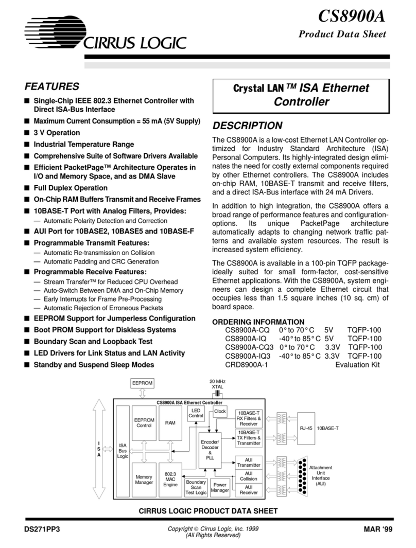
Cirrus Logic Crystal LAN CS8900A Installation and operating instructions

Application Note
&U\VWDO/$1 CS8900A ETHERNET CONTROLLER
TECHNICAL REFERENCE MANUAL
By Deva Bodas
Revised by James Ayres

AN83REV3
SCHEMATIC CHECKLIST
Before getting into the meat of the technical refer-
ence manual here is a schematic checklist. It’s pre-
sented here, at the beginning, to help the hardware
designer implement the design quickly and easily.
-No caps across the crystal. The CS8900A
implements these internally.
-4.99K 1% resistor between pin 93 and pin 94. A
common mistake is the resistor is connected to
Vcc instead of ground.
-RESET is active high, not active low.
-Check addressing.
-On non-ISA systems, if the processor is Big
Endian, it may be beneficial to byte swap the
data lines to minimize byte swapping in
software.
-SBHE (16 bit mode) -- must be low on IO or Mem
address. And it must toggle at least once to put
the CS8900 in 16 bit mode.
-IO and Memory Accesses: SBHE, AEN, etc.
must be stable for 10ns (read) and 20ns (write)
before access.
-IOCHRDY - Generally not connected in non-ISA
bus.
-CHIPSEL (active low). Tie to ground if not using
ELCS.
-Make sure interrupt line is active high. It is best
to put a pull down (10K) on INT line since
selected IRQ line is tristated during software
initiated reset.
-ELCS should be pulled to ground or left floating
if not used.
-EEDataIn should be pulled to ground if not used.
-10Base-T circuit -- no caps on TX lines between
isolation transformer and 10 Base-T connector.
-10Base-T circuit -- no center tap caps on
isolation transformer and 10 Base-T connector.
Good to have pads, don’t populate except for
EMI problems.
-Isolation transformer -- start with one that does
not have a common mode choke. If there are
EMI considerations, then use one with common
mode choke. The pin outs are the same. For
3.3V operation, use a transformer with 1:2.5
turns ration on TX and 1:1 on RX like the
YL18-1080S.
-For EMI problems, 1) add choke, 2) add center
tap caps on isolation transformer
-If using a shielded RJ45 connector, make sure
the shield pins are connected to chassis ground.
-AEN connected to ground if not using DMA.
-AEN can be used as an active low chip select if
not using DMA.
-AUI Interface -- use a 1AMP fuse. MAU can use
.5amps even better use a thermistor ("poly
switch"). Also, use a diode so can’t back-drive
from an externally powered MAU. Use a Halo
TnT integrated module to simplify 10Base2
interface.
-TX series termination resistors are R: 24.3 Ohm
1% (8 or 8.2 Ohm 1% for 3.3V)
-RX shunt termination resistor is 100 Ohm
-Put a 68pF shunt across TX on primary side
(560pF for 3.3V)
-Don’t use split analog/digital power and ground
planes.
-Void ground/power plane from transformer to
RJ45
-Put .1uF cap on each supply pin very close to
CS8900
The schematic checklist and the example connec-
tion diagrams to the Hitachi SH3, Cirrus Logic CL-
PS7211 and the Motorola MC68302 microproces-
sors should make clear the necessary the hardware
connections for a wide variety of situations.

AN83REV3
INTRODUCTION TO CS8900A
TECHNICAL REFERENCE MANUAL
This Technical Reference Manual provides the in-
formation which will be helpful in designing a
board using the CS8900A, programming the asso-
ciated EEPROM, and installing and running the
CS8900A device drivers. It is expected that the
user of this technical reference manual will have a
general knowledge of hardware design, Ethernet,
the ISA bus, and networking software. Recom-
mended sources of background information are:
ISA System Architecture by Shanley and
Anderson, Mindshare Press, 1992, ISBN 1-
881609-05-7
Ethernet, Building a Communication Infra-
structure, by Hegering and Lapple, Addison-
Wesley, 1993, ISBN 0-201-62405-2
Netware Training Guide: Networking Technol-
ogies, by Debra Niedenmiller-Chaffis, New
Riders Publishing, ISBN 1-56205-363-9
As shown in the Figure 1, the CS8900A requires a
minimum number of external components. The
EEPROM stores configuration information such as
interrupt number, DMA channel, I-O base address,
memory base address, and IEEE Individual Ad-
dress. The EEPROM can be eliminated on a PC
motherboard if that information in stored in the sys-
tem CMOS. Note also that the Boot PROM is only
needed for diskless workstations that boot DOS at
system power up, over the network. Also, the LEDs
are optional.
The hardware design considerations for both moth-
erboards and adapter cards are discussed in
“HARDWARE DESIGN”on page 7. The EE-
PROM programming considerations are described
in “JUMPERLESS DESIGN”on page 45.
Cirrus provides a complete set of device drivers, as
discussed in “DEVICE DRIVERS AND SET-
UP/INSTALLATION SOFTWARE”on page 56.
The drivers reside between the networking operat-
ing system (NOS) and the CS8900A. On the
CS8900A side, the drivers understand how to pro-
Boundary
RAM
ISA
Bus
Logic
Memory
Manager
Media Access
Control
(MAC).
Ethernet
protocol
processing.
EEPROM
Control
Encoder,
Decoder
&
PLL
10BASE-T
RX Filters &
Receiver
10BASE-T
TX Filters &
Transmitter
AUI
Transmitter
AUI
Collision
AUI
Receiver
Clock
Power
Manage
Scan
Test Logic
LED
Control
EEPROM:
Stores Configuration
Information &
IEEE Address
57
pins
ISA Bus
Boot PROM:
Used to boot diskless
workstations.
AUI
Transformer
(Attachment
Unit
Interface)
10BASE-T
Transformer
Figure 1. Hardware Application Summary

AN83REV3
LINK
ACTIVITY
D0
D1
D2
D3
D4
D5
D6
D7
D8
D9
D10
D11
D12
D13
D14
D15
nMWE
nMOE
A1
A2
A3
nCS2
CS8900_RST
D[15:0]
A[3:1]
CS8900_RSTnURESET
EINT3
VDD
VDD
VDD
VDD
VDD VDDVDD VDDVDD
VDD
VDD
VDD
VDD
VDD
GND
GND
GND
GND
GND
GND GND GND GND GND GND GND
C62
560pF
R97
100K
U21
CS8900A
93
37
38
39
40
41
42
43
44
45
46
47
48
50
51
52
53
54
58
59
60
65
66
67
68
71
72
73
74
27
26
25
24
21
20
19
18
7
28
29
62
61
49
36
63
75
77
76
2
3
4
5
6
97
98
99
78
100
84
83
82
81
80
79
92
91
88
87
32
31
30
35
34
33
64
15
13
11
16
14
12
17
9
22
56
698
10
23
55
57
70
1
89
86
94
96
90
85
95
RES
SA0
SA1
SA2
SA3
SA4
SA5
SA6
SA7
SA8
SA9
SA10
SA11
SA12
SA13
SA14
SA15
SA16
SA17
SA18
SA19
SD0
SD1
SD2
SD3
SD4
SD5
SD6
SD7
SD8
SD9
SD10
SD11
SD12
SD13
SD14
SD15
CHIPSEL
MEMW
MEMR
IOW
IOR
REFRESH
SBHE
AEN
RESET
SLEEP
TESTSEL
ELCS
EECS
EESK
EEDATAOUT
EEDATAIN
XTLI
XTLO
LED0/HC0
BSTATUS/HC1
LANLED
DO-
DO+
CI-
CI+
DI-
DI+
RXD-
RXD+
TXD-
TXD+
INTRQ0
INTRQ1
INTRQ2
INTRQ3
MEMCS16
IOCS16
IOCHRDY
DMARQ0
DMARQ1
DMARQ2
DMACK0
DMACK2
DMACK3
CSOUT
VCC
VCC
VCC
VCCGND
GND
GND
GND
GND
GND
AVSS0
AVSS1
AVSS2
AVSS3
AVSS4
AVDD1
AVDD2
AVDD3
R94
8R
R95
8R
R96
4K99 1%
X3
20MHz
R91
4K7
R89
390R
C89
100nF
C90
100nF
R93
100R
D7
LED
2 1
C93
100nF
C92
100nF
C94
100nF
R90
390R
D6
LED
2 1
C88
100nF
U30A
74LVX04
1 2
C91
100nF
D[15:0]
A[3:1]
nMWE
nMOE
nCS2
nURESET
RxD-
RxD+
TxD-
TxD+
Figure 4. CS8900A Interface to Cirrus Logic CL-PS7211

AN83REV3
SH3 A2
SH3 IRQ0
RESET
SH3 RO#
Chip Select#
SH3 WE1#
SH3 [D15:D0]
SH3 A1
SH3 A3
RDX-
RXD+
TXD-
TXD+
3.3V
3.3V
3.3V
3.3V
510
0.1uF
510
CS8900A-CQ3
37
38
39
40
41
42
43
44
45
46
47
48
50
51
52
53
54
58
59
60
65
66
67
68
71
72
73
74
27
26
25
24
21
20
19
18
28
29
62
61
49
63
75
34
33
64
32
31
30
35
15
13
11
16
14
12
3
6
5
4
9
22
56
69
90
85
95
8
10
23
55
57
70
1
89
86
94
96
77
76
93
84
83
80
79
82
81
92
91
88
87
78
99
100
17
97
98
2
7
36
SA0
SA1
SA2
SA3
SA4
SA5
SA6
SA7
SA8
SA9
SA10
SA11
SA12
SA13
SA14
SA15
SA16
SA17
SA18
SA19
SD0
SD1
SD2
SD3
SD4
SD5
SD6
SD7
SD8
SD9
SD10
SD11
SD12
SD13
SD14
SD15
MEMW
MEMR
IOW
IOR
REFRESH
AEN
RESET
MEMCS16
IOCS16
IOCHRDY
INTRQ0
INTRQ1
INTRQ2
INTRQ3
DMARQ0
DMARQ1
DMARQ2
DMACK0
DMACK1
DMACK2
EECS
EEDATAIN
EEDATAOUT
EESK
DVDD1
DVDD2
DVDD3
DVDD4
AVDD1
AVDD2
AVDD3
DVSS1
DVSS1A
DVSS2
DVSS3
DVSS3A
DVSS4
AVSS0
AVSS1
AVSS2
AVSS3
AVSS4
HWSLEEP
TESTSEL
RES
DO-
DO+
DI-
DI+
CI-
CI+
RXD-
RXD+
TXD-
TXD+
BSTATUS/HC1
LINKLED/HC0
LANLED
CSOUT
XTAL1
XTAL2
ELCS
CHIPSEL
SBHE
LED
4.99K
0.1uF
LED
0.1uF
20MHz
0.1uF
0.1uF
0.1uF
0.1uF
560pF
8
8
100
Figure 5. CS8900A Interface to Hitachi SH3

18 AN83REV3
PROM is not necessary for the CS8900A, and the
CS8900A will respond to IO addresses 0300h
through 030Fh after a reset.
Please refer to the CS8900A data sheet for informa-
tion about programming the EEPROM. Please re-
fer to “JUMPERLESS DESIGN”on page 45 of
this document for information about EEPROM in-
ternal word assignments.
LEDs
Many embedded systems do not require LEDs for
the Ethernet traffic. Therefore this reference de-
sign does not implement any LEDs. However, the
CS8900A has direct drives for the three LEDs.
Please refer to the data sheet for the CS8900A for a
description of the LED functions available on the
CS8900A.
10BASE-T Interface
The 10BASE-T interface for the CS8900A is
straight forward. Please refer to Figure 8 (3.3V)
and Figure 10 (5V) for connections and compo-
nents of this circuit. Transmit and receive signal
lines from the CS8900A are connected to an isola-
tion transformer at location T1. This isolation
transformer has a 1:1 ratio between the primary and
the secondary windings on the receive side. It has
a 1:√2 (1:1.414) ratio between the primary and the
secondary windings for the transmit lines for 5V
operation or a ratio of 1:2.5 for 3.3V operation. Re-
sistor R1 provides termination for the receive lines.
Resistors R2 and R3 are in series with the differen-
tial pair of transmit lines for impedance matching.
10BASE-2 and AUI Interfaces
As many embedded systems require only a
10BASE-T interface, this reference design imple-
ments only the 10BASE-T interface. However,
should a user require a 10BASE-2 or AUI inter-
face, the CS8900A provides a direct interface to the
AUI. Please refer to “Low Cost Ethernet Combo
Card Reference Design: CRD8900”on page 21 of
this document for details about the AUI interface.
Logic Schematics
Figures 8, 9 and 10 detail the logic schematics for
the various circuits used in the reference design.
10BT_RD-
100
R2
8
R4
8
R5
.1uF .1uF
C23
.1uF 2KV
C28
.1uF 2KV
C29
1
1
2
2
3
3
44
5
5
6
6
7
7
8
8
1
2
3
4
5
6
7
8
16
(1-3) (16-14) 1:1
(6-8) (11-9) 1:2.5
10BaseT Transformer
15
14
13
12
11
10
10
J21
9
16
15
14
13
12
11
10
9
9
Do Not
Populate
560pF
C30
10BT_RD+
10BT_TD-
10BT_TD+
Do Not
Populate
Figure 8. 10BASE-T Schematic 3.3V

AN83REV3
SA00
SA01
SA02
SA03
SA04
SA05
SA06
SA07
SA08
SA09
SA10
SA11
SA12
SA13
SA14
SA15
SA16
SA17
SA18
SA19
ISA0
ISA1
ISA2
ISA3
ISA4
ISA5
ISA6
ISA7
ISA8
ISA9
ISA10
ISA11
ISA12
ISA13
ISA14
ISA15
ISA16
ISA17
ISA18
ISA19
37
38
39
40
41
42
43
44
45
46
47
48
50
51
52
53
54
58
59
60
CHIPSEL
MEMW
MEMR
IOW
IOR
REFRESH
SBHE
AEN
7
28
29
62
61
49
36
63
SMEMW
SMEMR
IOW
IOR
REFRESH
SBHE
AEN
76
77
75
TSTSEL
RESET
TESTSEL
SLEEP
RESET
+5V
XTAL
20.0 MHz
X1
1
2
97
98
93
XTL1
XTL2
RES
R4
4.99k, 1%
ELCS
DVSS3A
DVSS1A
DVSS4
DVDD4
DVSS3
DVDD3
DVSS2
DVDD2
DVSS1
DVDD1
AVSS3
AVDD3
AVSS2
AVDD2
AVSS1
AVDD1
AVSS4
AVSS0
EEDATAIN
EESK
2
57
10
70
69
55
56
23
22
8
9
94
95
86
85
89
90
96
1
6
4
C12
C14
C13
C9
C8
C11
C10
0.1
µ
F
+5V
EE_CLK
+5V
0.1
µ
FC7
1
2
3
5
8
4
7
6
VCC
D0
NC2
NC1
1K_EEPROM_S
CS
CLK
D1
VSS
U3
EECS
EEDATAOUT
3
5
12
U1
CS8900
RXD+
TXD-
TXD+
INTRQ0
INTRQ1
INTRQ2
INTRQ3
MEMCS16
I0CS16
I0CHRDY
DMARQ0
DMARQ1
DMARQ2
CSOUT
91
88
87
32
31
30
35
34
33
64
15
13
11
17
10BT_RD+
10BT_TD-
10BT_TD+
IRQ10
IRQ11
IRQ12
IRQ5
MEMCS16
I0CS16
I0CHRDY
DRQ5
DRQ6
DRQ7
ISA_D0
ISA_D1
ISA_D2
ISA_D3
ISA_D4
ISA_D5
ISA_D6
ISA_D7
ISA_D8
ISA_D9
ISA_D10
ISA_D11
ISA_D12
ISA_D13
ISA_D14
ISA_D15
65
66
67
68
71
72
73
74
27
26
25
24
21
20
19
18
SD0
SD1
SD2
SD3
SD4
SD5
SD6
SD7
SD8
SD9
SD10
SD11
SD12
SD13
SD14
SD15
DMACK0
DMACK2
DMACK3
16
14
12
DACK5
DACK6
DACK7
80
79
82
81
84
83
78
100
99
RXD- 92 10BT_RD-
DI-
DI+
CI-
CI+
DO-
DO+
BSTATUS / HC1
LED2
LED0/HC0
0.1
µ
F
0.1
µ
F
0.1
µ
F
0.1
µ
F
0.1
µ
F
0.1
µ
F
Figure 9. Overall Schematic

AN83REV3
Component Placement and Signal Routing
Please refer to “Layout Considerations for the
CS8900A”on page 35 of this document for more
details on the placement of components on the
board. It is important to provide very clean and ad-
equate +5 V and ground connections to the
CS8900A.
Bill of Material
Table 1 has a list components that are typically
used to assemble this adapter card. For most of the
components, there are several alternative manufac-
turers.
1
2
3
4
5
6
7
8
2
3
4
5
6
7
89
10
11
12
13
14
15
16
9
10
11
12
13
14
15
16
(1-3) (16-14) 1:1
(6-8) (11-9) 1:1.414
10 BaseT Transformer
100
R2
24.3
R4
24.3
R5
68 pF
C30
.1
µ
F
C23
Do Not
Populate
.1
µ
F 2KV
C29
.1
µ
F 2KV
C28
J1
10
8
7
6
5
4
3
2
1
9
.1
µ
F
Do Not
Populate
10BT_RD-
10BT_RD+
10BT_TD-
10BT_TD+
Figure 10. 10BASE-T Schematic 5V
C17
TANT TANT TANT
22
µ
F22
µ
F22
µ
F
C16 C15
+
+5V
GND
++
Figure 11. Decoupling Capacitors Schematic
Item Reference # Description Quantity Vendor Part Number
1 C2, C5, C7..C14 Capacitor, 0.1 µF, X7R, SMT0805 10
2 C15, C16, C17 Capacitor, 22 µF, SMT7343 3
3 R2, R3 Resistor, 24.3, 1%, 1/8W, SMT0805 2
4 R1 Resistor, 100, 1%, 1/8W, SMT0805 1
5 R4 Resistor, 4.99K, 1%, SMT0805 1
6* X1 Crystal, 20.000 MHz 1 M-tron ATS-49,20.000 MHz,18 pF
7 J1 Connector, RJ45, 8 pin 1 AMP 555164-1
8
9 U1 ISA Ethernet Controller 1 Crystal CS8900A
10* U3 1K EEPROM 1 Microchip 93C46 (8 pin SOIC)
* Depending on system resources, these parts may not be needed.
Table 1. CS8900A Design Bill of Materials
T1 Transformer,2,1:1,1:1.41 1YUTAI YL18-1064S

AN83REV3
SA00
SA01
SA02
SA03
SA04
SA05
SA06
SA07
SA08
SA09
SA10
SA11
SA12
SA13
SA14
SA15
SA16
SA17
SA18
SA19
ISA0
ISA1
ISA2
ISA3
ISA4
ISA5
ISA6
ISA7
ISA8
ISA9
ISA10
ISA11
ISA12
ISA13
ISA14
ISA15
ISA16
ISA17
ISA18
ISA19
37
38
39
40
41
42
43
44
45
46
47
48
50
51
52
53
54
58
59
60
CHIPSEL
MEMW
MEMR
IOW
IOR
REFRESH
SBHE
AEN
7
28
29
62
61
49
36
63
CHIPSEL
MEMW
MEMR
IOW
IOR
REFRESH
SBHE
AEN
76
77
75
TSTSEL
RESET
TESTSEL
SLEEP
RESET
+5V
XTAL
20.0 MHz
X1
12
ELCS
97
98
93
XTL1
XTL2
RES
R3
4.99k
ELCS
DVSS3A
DVSS1A
DVSS4
DVDD4
DVSS3
DVDD3
DVSS2
DVDD2
DVSS1
DVDD1
AVSS3
AVDD3
AVSS2
AVDD2
AVSS1
AVDD1
AVSS4
AVSS0
EEDATAIN
EESK
2
57
10
70
69
55
56
23
22
8
9
94
95
86
85
89
90
96
1
6
4
C16
C17
C8
C7
C11
C13
C12
0.1
µ
F
+5V
EE_CLK
EE_DIN
EE_CLK
+5V
0.1
µ
F
C5
1
2
3
5
8
4
7
6
VCC
D0
NC2
NC1
1K_EEPROM_S
CS
CLK
D1
VSS
U3
EECS
EEDATAOUT
3
5
12
U1
CS8900
RXD-
RXD+
TXD-
TXD+
INTRQ0
INTRQ1
INTRQ2
INTRQ3
MEMCS16
I0CS16
I0CHRDY
DMARQ0
DMARQ1
DMARQ2
CSOUT
92
91
88
87
32
31
30
35
34
33
64
15
13
11
17
PROM CS
10BT_RD-
10BT_RD+
10BT_TD-
10BT_TD+
IRQ10
IRQ11
IRQ12
IRQ5
MEMCS16
I0CS16
I0CHRDY
DRQ5
DRQ6
DRQ7
PROM_CS
ISA_D0
ISA_D1
ISA_D2
ISA_D3
ISA_D4
ISA_D5
ISA_D6
ISA_D7
ISA_D8
ISA_D9
ISA_D10
ISA_D11
ISA_D12
ISA_D13
ISA_D14
ISA_D15
65
66
67
68
71
72
73
74
27
26
25
24
21
20
19
18
SD0
SD1
SD2
SD3
SD4
SD5
SD6
SD7
SD8
SD9
SD10
SD11
SD12
SD13
SD14
SD15
DMACK0
DMACK2
DMACK3
16
14
12
DACK5
DACK6
DACK7
DI-
DI+
80
79
CI-
CI+
82
81
DO-
DO+
84
83
DI-
DI+
CI-
CI+
DO-
DO+
BSTATUS / HC1
LED2
78
100
LED0/HC0
99
BSTATUS / HC1
R18
680
R19
680
3
1
4
2
LED_T
LED_B
0.1
µ
F
0.1
µ
F
0.1
µ
F
0.1
µ
F
0.1
µ
F
0.1
µ
F
Figure 13. CS8900A Schematic (Combo Card Application)

AN83REV3
Figure 14. Power Supply Decoupling Schematic
Figure 15. Boot PROM Schematic
C19
TANT TANT TANT
22
µ
F22
µ
F22
µ
F
C10 C1
+
+5V
GND
++
SA00
SA01
SA02
SA03
SA04
SA05
SA06
SA07
SA08
SA09
SA10
SA11
SA12
SA13
SA14
A0
A1
A2
A3
A4
A5
A6
A7
A8
A9
A10
A11
A12
A13
A14
10
9
8
7
6
5
4
3
25
24
21
23
2
26
27
DQ7
DQ6
DQ5
DQ4
DQ3
DQ2
DQ1
DQ0
27C256
CE
OE
VPP
PROM_CS
1
22
20
19
18
17
16
15
13
12
11
PD7 2
PD6 3
PD5 4
PD4 5
PD3 6
PD2 7
PD1 8
PD0 9
A1
A2
A3
A4
A5
A6
A7
A8
B1
B2
B3
B4
B5
B6
B7
B8
18
17
16
15
13
12
11
14
OE
DIR
1
19
R1
4.7k
+5V
C4
0.1
µ
F
U7
SD7
SD6
SD5
SD4
SD3
SD2
SD1
SD0
74LS245
U6
C2
0.1
µ
F

AN83REV3
Figure 16. AUI Schematic
Figure 17. 10BASE-2 Schematic
Figure 18. PAL Decode of LA[20-23]
+12V
0.1
µ
F
BSTATUS/HCI
1
2
4
5
7
8
16
15
13
12
10
9
AUI_XFR_S
T1
I11
I12
I21
I22
I31
I32
O11
O12
O21
O22
O31
O32
DO+
CI-
CI+
DI-
DI+
DO-
14
13
12
4
3
2
TX+
RX-
RX+
CD-
CD+
C18
0.1
µ
F
1
2
3
22
23
24
+12IN1
+12IN2
EN
EN
-12IN1
-12IN2
SOUT+
SOUT-
12
9
13
NC
U5
DC-DC
CONVERSION
C21
0.1
µ
F
ISOLATED_GND
-9_V
1082 DO-
1082 DO+
1082 DI-
1082 DI+
1082 CI-
1082 CI+
R10 1K
TX-
HBE
RR+
RR-
VEE5
VEE4
VEE3
VEE2
VEE1
VEE6
VEE9
VEE8
VEE7
VEE10
VEE12
VEE11
VEE13
18
15
19
10
9
8
7
6
5
20
11
23
22
21
25
24
CDS
TX0
RX1
GND1
GND2
NC
1
28
26
16
17
27
CS83C92C_S
U2
CDS
TX0
RX1
D1
1H916
C20
R15 10k R16 121
J3
BNC_50
1
2
C24
1kV
.01
µ
F
1M
1/2W
R17
DO-
DO+
CI-
CI+
DI-
DI+
R6 39.2
R8
39.2
Ω
R9 39.2
R7 39.2
C14
CI-
CI+
DI-
DI+
0.1
µ
F
C15
1
2
4
5
7
8
16
15
13
12
10
9
AUI_XFR_S
T2
1
2
3
4
5
6
7
8
CI_A
DO_A
DI_A
CON_AUI15PSUBO
J2
9
10
11
12
13
14
15
16 17
CI_B
DO_B
DI_B
0.1
µ
F
C27
+12V F1 VP_+12V
I11
I12
I21
I22
I31
I32
O11
O12
O21
O22
O31
O32
0.1
µ
F
1
11
2
3
4
5
6
7
8
9
CLK
G
10
11
12
13
14
15
16
17
I/00
I/01
I/02
I/03
12
13
18
19
14
15
16
17
00
01
02
03
CHIPSEL_B (CS8900 Pin7)
PAL16R4
ELCS
EEDOUT
BALE
LA23
LA22
LA21
LA20
RESET
EE_SK
(CS8900 Pin2)
CS8900 Pin5)
(ISA B28)
(ISA C02)
(ISA C03)
(ISA C04)
(ISA C05)
(ISA B02)
(CS8900 Pin 4)
YL18-1005D
YL18-1005D
Other manuals for Crystal LAN CS8900A
2
Table of contents
Other Cirrus Logic Controllers manuals
