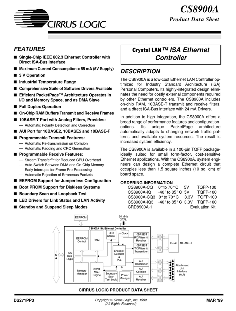
Cirrus Logic CRYSTAL LAN CS890 Product manual

#RYSTAL,!.×
CS8900
Ethernet Controller
Technical Reference Manual
Version: 1.31
AN83REV1
September 10, 1996
Copyright © Crystal Semiconductor Corporation, 1996
(All Rights Reserved)
To obtain technical application support, call (800) 888-5016 (from the US and Canada) or
512-442-7555 (from outside the US and Canada), and ask for CS8900 Application Support,

2 AN83REV1
CS8900 Technical Reference Manual
The information contained in this document is subject to change without notice. Crystal Semiconductor Corpora-
tion makes no warranty of any kind with regard to this material including, but not limited to, the implied warran-
ties of merchant ability and fitness for a particular purpose. Crystal Semiconductor Corporation shall not be liable
for errors contained herein or for incidental or consequential damages in connection with the furnishing, perform-
ance, or use of this material.
This Equipment has been tested and found to comply with the limits for a Class B digital device, pursuant to Part
15 of the FCC Rules. These limits are designed to provide reasonable protection against harmful interference in a
residential installation. This equipment generates, uses, and can radiate radio frequency energy and, if not in-
stalled and used in accordance with the instructions, may cause harmful interference to radio communications.
However, there is no guarantee that interference will not occur in a particular installation. If this equipment does
cause harmful interference to radio or television reception, which can be determined by turning the equipment off
and on, the user is encouraged to try to correct the interference by one or more of the following:
•Reorient or relocate the receiving antenna.
•Increase the separation between the equipment and the receiver.
•Consult the dealer or an experienced radio/TV technician for help.
This equipment must be used with shielded interface cables. If shielded interface cables are not used, this unit will
not comply with FCC specifications and is prohibited.
This document contains information which is protected by copyright. All rights reserved. No part of this docu-
ment may be photocopied, reproduced, or translated to another language without the prior written consent of
Crystal Semiconductor Corporation.
The following are trademarks of Crystal Semiconductor: StreamTransfer, PacketPage, and SMART Analog
Other trademarks used in thisTechnical Reference Manual include:
Ethernet is a registered trademark of Xerox Corp.
Artisoft and LANtastic are registered trademarks of Artisoft, Inc.
Banyan and VINES are registered trademarks of Banyan Systems.
Digital and PATHWORKS are registered trademarks of Digital Equipment Corporation.
Intel is a registered trademark of Intel Corporation.
LAN Server and IBM are registered trademarks of International Business Machines Corp.
Microsoft, LAN Manager, Windows 95, Windows for Workgroups, and Windows NT are registered trademarks
of Microsoft.
Novell and Netware are registered trademarks of Novell, Inc.
SCO is a registered trademark of Santa Cruz Organization, Inc.
UNIX is a registered trademark of AT&T Technologies, Inc.
Other product names may be trademarks of their respective companies.

AN83REV1 3
CS8900 Technical Reference Manual
TABLE OF CONTENTS
CRYSTAL LAN™ CS8900 ETHERNET CONTROLLER TECHNICAL REFERENCE
MANUAL..................................................................................................................................1
1.0 INTRODUCTION TO CS8900 TECHNICAL REFERENCE MANUAL.....................6
2.0 HARDWARE DESIGN.....................................................................................................9
2.1 ETHERNET HARDWARE DESIGN FOREMBEDDED SYSTEMS AND MOTHERBOARDS .................9
2.1.1 General Description .....................................................................................................9
2.1.2 Board Design Considerations ......................................................................................9
2.1.2.1 Crystal Oscillator................................................................................................................................................ 9
2.1.2.2 ISA Bus Interface............................................................................................................................................... 9
2.1.2.3 External Decode Logic ....................................................................................................................................... 9
2.1.2.4 EEPROM ..........................................................................................................................................................10
2.1.2.5 LEDs.................................................................................................................................................................10
2.1.2.6 10BASE-T Interface..........................................................................................................................................10
2.1.2.7 10BASE-2 and AUI Interfaces...........................................................................................................................10
2.1.3 Logic Schematics ........................................................................................................11
2.1.4 Component Placement and Signal Routing ................................................................11
2.1.5 Bill of Material ...........................................................................................................11
2.2 LOW COST ETHERNET COMBO CARD REFERENCE DESIGN: CRD8900 ................................16
2.2.1 General Description ...................................................................................................16
2.2.2 Board Design..............................................................................................................16
2.2.2.1 Crystal Oscillator...............................................................................................................................................16
2.2.2.2 ISA Bus Interface..............................................................................................................................................16
2.2.2.3 External Decode Logic ......................................................................................................................................16
2.2.2.4 EEPROM ..........................................................................................................................................................16
2.2.2.5 Socket For Optional Boot PROM ......................................................................................................................17
2.2.2.6 LEDs.................................................................................................................................................................18
2.2.2.7 10BASE-T Interface..........................................................................................................................................18
2.2.2.8 AUI Interface ....................................................................................................................................................18
2.2.2.9 10BASE-2 Interface ..........................................................................................................................................18
2.2.3 Logic Schematics ........................................................................................................19
2.2.4 Component Placement and Routing of Signals ..........................................................19
2.2.5 Bill of Material ...........................................................................................................19
2.3 ADDRESSING THECS8900: I/O MODE, MEMORY MODE.......................................................28
2.3.1 I/O mode.....................................................................................................................28
2.3.2 Memory mode .............................................................................................................28
2.3.2.1 Lower Memory mode........................................................................................................................................28
2.3.2.2 Extended Memory mode....................................................................................................................................29
2.4 LAYOUT CONSIDERATIONS FOR THECS8900.......................................................................33
2.4.1 General guidelines .....................................................................................................33
2.4.2 Power supply connections ..........................................................................................33
2.4.2.1 Two layered printed circuit board (PCB)............................................................................................................35
2.4.2.2 Multi-layered printed circuit board.....................................................................................................................35
2.4.3 Routing of the digital signals .....................................................................................45

4 AN83REV1
CS8900 Technical Reference Manual
2.4.4 Routing of the analog signals .....................................................................................45
2.5 RECOMMENDED MAGNETICS FOR THECS8900 ...................................................................47
3.0 JUMPERLESS DESIGN .................................................................................................50
3.1 SERIAL EEPROM................................................................................................................50
3.1.1 Reset Configuration Block ..........................................................................................50
3.1.2 Driver Configuration Information ..............................................................................51
3.1.3 Format of Driver Configuration Block .......................................................................51
3.1.3.1 IEEE Physical Address......................................................................................................................................54
3.1.3.2 ISA Configuration Flags.................................................................................................................................... 54
3.1.3.3 PacketPage Memory Base.................................................................................................................................. 55
3.1.3.4 Boot PROM Memory Base .............................................................................................................................. 55
3.1.3.5 Boot PROM Mask ...........................................................................................................................................55
3.1.3.6 Transmission Control........................................................................................................................................55
3.1.3.7 Adapter Configuration Word.............................................................................................................................55
3.1.3.8 EEPROM Revision............................................................................................................................................ 56
3.1.3.9 Manufacturing Date ..........................................................................................................................................56
3.1.3.10 IEEE Physical Address (copy).........................................................................................................................56
3.1.3.11 16-bit Checksum.............................................................................................................................................56
3.1.3.12 EISA ID..........................................................................................................................................................56
3.1.3.13 Serial Number..................................................................................................................................................57
3.1.3.14 Serial ID Checksum.........................................................................................................................................57
3.1.4 Maintaining EEPROM Information ...........................................................................57
3.2 MOTHERBOARD DESIGNS....................................................................................................57
3.2.1 BIOS-Based Design Considerations.............................................................................57
3.2.2 Driver Interface with BIOS-Based Configuration ......................................................58
3.3 OBTAINING IEEE ADDRESSES ............................................................................................60
4.0 DEVICE DRIVERS AND SETUP/INSTALLATION SOFTWARE............................61
4.1 CRYSTAL’S SOFTWARE LICENSING PROCEDURES .................................................................61
4.2 CONTENTS OF FLOPPY DISKS INCLUDED WITH THISKIT......................................................61
4.3 DOS SETUP AND INSTALLATIONUTILITY ...........................................................................66
4.3.1 Installation Procedure ...............................................................................................66
4.3.1.1 Adapter/Auto Configuration Screen................................................................................................................... 67
4.3.1.2 Adapter/Manual Configuration Screen...............................................................................................................67
4.3.1.3 Diagnostics/Self Test Screen.............................................................................................................................68
4.3.1.4 Driver/Install Screen..........................................................................................................................................69
4.3.1.5 Diagnostics/Network Test Screen......................................................................................................................69
5.0 CS8900: LOW COST, HIGH PERFORMANCE ETHERNET CONTROLLER FOR
NON-ISA SYSTEMS..............................................................................................................71
5.1 THE CS8900 ARCHITECTURE...............................................................................................71
5.1.1 ISA bus ........................................................................................................................71
5.1.2 CS8900 in IO mode .....................................................................................................71
5.1.3 CS8900 in memory mode.............................................................................................72
5.1.4 DMA interface of the CS8900 .....................................................................................72
5.2 SELECTION OF IO, MEMORY ANDDMA MODES...................................................................73
5.3 DESIGN EXAMPLE: CS8900 INTERFACE TO MC68302..........................................................74

AN83REV1 5
CS8900 Technical Reference Manual
5.3.1 Address Generation .....................................................................................................74
5.3.2 Read and write signals ................................................................................................75
5.3.3 SBHE* signal ..............................................................................................................75
5.3.4 Other control signals...................................................................................................75
5.3.5 Status signals from CS8900 .........................................................................................75
5.4 DATABUS (SD[0:15]) CONNECTION.....................................................................................75
5.5 CHECKLIST FOR SIGNAL CONNECTIONS TO THECS8900........................................................76
5.6 IS THE EEPROM NECESSARY?.............................................................................................76
5.7 SUMMARY ...........................................................................................................................77
6.0 CONTACTING CUSTOMER SUPPORT AT CRYSTAL ...........................................78
6.1 CRYSTAL BBS.....................................................................................................................78
6.1.1 Connecting to the BBS.................................................................................................78
6.1.2 Guests..........................................................................................................................78
6.1.3 Registered Callers .......................................................................................................78
7.0 INDEX...............................................................................................................................79

6 AN83REV1
CS8900 Technical Reference Manual
1.0 Introduction to CS8900 Techni-
cal Reference Manual
This Technical Reference Manual provides
the information which will be helpful in
designing a board using the CS8900, pro-
gramming the associated EEPROM, and
installing and running the CS8900 device
drivers. It is expected that the user of this
technical reference manual will have a gen-
eral knowledge of hardware design, Ether-
net, the ISA bus, and networking software.
Recommended sources of background in-
formation are:
a) ISA System Architectureby Shanley
and Anderson, Mindshare Press, 1992,
ISBN 1-881609-05-7
b) Ethernet, Building a Communication
Infrastructure, by Hegering and Lapple,
Addison-Wesley, 1993, ISBN 0-201-
62405-2
c) Netware Training Guide: Networking
Technologies, by Debra Niedenmiller-
Chaffis, New Riders Publishing, ISBN
1-56205-363-9
As shown in the Figure 1.1, the CS8900
requires a minimum number of external
components. The EEPROM stores configu-
ration information such as interrupt num-
ber, DMA channel, I-O base address, mem-
ory base address, and IEEE Individual Ad-
dress. The EEPROM can be eliminated on
a PC motherboard if that information in
stored in the system CMOS. Note also that
the Boot PROM is only needed for diskless
workstations that boot DOS at system
power up, over the network. Also, the LEDs
are optional.
Figure 1.1 - Hardware Application Summary
Boundary
RAM
ISA
Bus
Logic
Memory
Manager
Media Access
Control
(MAC).
Ethernet
protocol
processing.
EEPROM
Control
Encoder,
Decoder
&
PLL
10BASE-T
RX Filters &
Receiver
10BASE-T
TX Filters &
Transmitter
AUI
Transmitter
AUI
Collision
AUI
Receiver
Clock
Power
Manage
Scan
Test Logic
LED
Control
EEPROM:
Stores Configuration
Information &
IEEE Address
57
pins
ISA Bus
Boot PROM:
Used to boot diskless
workstations.
AUI
Transformer
(Attachment
Unit
Interface)
10BASE-T
Transformer

AN83REV1 7
CS8900 Technical Reference Manual
The hardware design considerations for
both motherboards and adapter cards are
discussed in Chapter 2.0. The EEPROM
programming considerations are described
in Chapter 3.0.
Crystal provides a complete set of device
drivers, as discussed in Chapter 4.0. The
drivers reside between the networking op-
erating system (NOS) and the CS8900. On
the CS8900 side, the drivers understand
how to program and read the CS8900 con-
trol and status registers, and how to transfer
user data between the CS8900 and the PC
main memory via the ISA bus. On the
NOS side, the drivers provide the standard-
ized services and functions required by the
NOS, and hide all details of the CS8900
hardware from the NOS. The EEPROM
device programs the CS8900 whenever the
a hardware reset occurs, and call also store
state/configuration information for the
driver.
Crystal’s Software Driver (
#RYSTAL ,!.
TM)
Distribution Policy is as follows. The
CS8900 developer kit contains a single-
user copy of object code which is available
only for internal testing and evaluation
purposes. This object code may not be dis-
tributed without first signing a LICENSE
FOR DISTRIBUTION OF EXECUTABLE
SOFTWARE, which may be obtained by
contacting your sales representative. The
LICENSE FOR DISTRIBUTION OF EX-
ECUTABLE SOFTWARE gives you un-
limited, royalty-free rights to distribute
Crystal-provided object code.
The drivers supported are shown in Table
1.1.
Applications
Operating System Software
e.g., File Manager
Network Operating System
e.g., Novell or Microsoft
CS8900 - specific device drivers:
e.g., NDIS & ODI compatible drivers
CS8900 Registers & Memory EEPROM
Figure 1.2 - Software Application Summary

8 AN83REV1
CS8900 Technical Reference Manual
Driver Operating System Network Operation System
DOS ODI 4.x Client DOS 6.2 to 3.3, Novell 4.X, 3.X
Win 3.1,
Windows for Workgroups 3.11
OS/2 ODI 4.x Client OS/2 2.2, 2.1, Warp Novell 4.X, 3.X
ODI 4.x Server Novell 4.X, 3.X
NDIS 2.x - DOS DOS 6.2 to 3.3 LAN Manager, LAN Server,
Win 3.1 Windows for Workgroups 3.11
DEC Pathworks
NDIS 2.x - OS/2 OS/2 2.2, 2.1, Warp LAN Manager, LAN Server,
Banyan Vines, LANtastic,
DEC Pathworks
NDIS 3.x Windows NT NT Server, NT Workstation,
Windows ‘95 Novell 4.X, 3.X, 2.X
Windows for Workgroups Banyan Server
Packet V1.09 DOS 6.2 to 3.3 TCP/IP stacks including:
PC/TCP, SUN PC-NFS,
Wollongong
SCO UNIX
LINUX
pSOS
Vx Works
Boot PROM Novell 4.X, 3.X, 2.X
LAN Manager, LAN Server,
Banyan Vines, LANtastic,
DEC Pathworks
Setup & Installation Utility DOS 6.2 to 3.3
Table 1.1 - Supported Drivers

AN83REV1 9
CS8900 Technical Reference Manual
2.0 Hardware Design
This section give design guidance for both
embedded and adapter card designs, includ-
ing recommendations for dealing with the
upper ISA address lines (LA[20:23]),
choosing transformers, and laying out the
board.
2.1 Ethernet Hardware Design for
Embedded Systems and Mother-
boards
This section describes the hardware design
of a four-layer, 10BASE-T solution in-
tended for use on PC motherboards, or in
other embedded applications. The goal of
this design is minimal board space and
minimal material cost. Therefore, a number
of features (BootPROM, AUI, 10BASE-2)
are not supported in this particular PCB
design. An example of this circuit is in-
cluded in this technical reference manual,
and is implemented in an ISA form factor.
This same circuit can be implemented di-
rectly on the processor PCB.
2.1.1 General Description
The small footprint, high performance and
low cost of the CS8900 Ethernet solution,
makes the CS8900 an ideal choice for em-
bedded systems like personal computer
(PC) mother boards. The very high level of
integration in the CS8900 results in a very
low component count Ethernet design.
This makes it possible to have a complete
solution fit in an area of 1.5 square inches.
Since the analog filters are integrated on
the CS8900, card may more easily be made
compliant with FCC part 15 class (B).
2.1.2 Board Design Considerations
2.1.2.1 Crystal Oscillator
The CS8900, in this reference design, uses
a 20.000 MHz crystal oscillator. The crys-
tal has a maximum load capacitance of 18
pF. The rest of the oscillator circuitry is
built internally to the CS8900. Please note
that the crystal must be placed very close to
XTL1 and XTL2 pins of the CS8900.
This crystal oscillator can be eliminated if
accurate clock signal (20.00 MHz +/-
0.01% and 45-55 duty cycle) available in
the system.
2.1.2.2 ISA Bus Interface
The CS8900 has a direct ISA bus interface.
Note that the ISA bus interface is simple
enough to allow the CS8900 to interface
with variety of micro-processors directly or
with the help of simple programmable logic
like a PAL or a GAL.
This reference design actually has the form
factor of an ISA adapter card. In this de-
sign, all the ISA bus connections from the
CS8900 are directly routed to the ISA con-
nector. The pin-out of the CS8900 is such
that if the CS8900 is placed as shown in
Figure 2.1.1, there will be almost no cross-
over of the ISA signals.
2.1.2.3 External Decode Logic
The CS8900 can be accessed in I/O mode
or memory mode. For this reference de-
sign, in memory mode the CS8900 is in the
conventional or upper memory of the PC.

10 AN83REV1
CS8900 Technical Reference Manual
That is, it resides in the lower 1 Mega bytes
of address space.
To use the CS8900 in extended memory
address space requires an external address
decoder. This decoder decodes upper 4 bits
(LA[20:23]) of 24 bit ISA address lines. In
many embedded microprocessors such de-
codes are available though the microproc-
essors itself.
Please refer to Section 2.3.2.2 for further
information.
2.1.2.4 EEPROM
A 64 word (64 X16 bit) EEPROM (location
U3) is used in the reference design to inter-
face with the CS8900. This EEPROM
holds the IEEE assigned Ethernet MAC
(physical) address for the board (see Sec-
tion 3.3). The EEPROM also holds other
configuration information for the CS8900.
The last few bytes of the EEPROM are
used to store information about the hard-
ware configuration and software require-
ments.
In an embedded system, such as a PC, the
system CMOS RAM or any other non-
volatile memory can be used to store the
IEEE address and Ethernet configuration
information. In such a case an EEPROM is
not necessary for the CS8900, and the
CS8900 will respond to IO addresses 0300h
through 030Fh after a reset.
Please refer to the section 3.5 and 3.6 of the
CS8900 data sheet for information about
programming the EEPROM. Please refer
to the Section 3.0 of this document for in-
formation about EEPROM internal word
assignments.
2.1.2.5 LEDs
Many embedded systems do not require
LEDs for the Ethernet traffic. Therefore
this reference design does not implement
any LEDs. However, the CS8900 has di-
rect drives for the three LEDs. Please refer
to the data sheet for the CS8900 for a de-
scription of the LED functions available on
the CS8900.
2.1.2.6 10BASE-T Interface
The 10BASE-T interface for the CS8900 is
straight forward. Please refer to Figure
2.2.5 for connections and components of
this circuit. Transmit and receive signal
lines from the CS8900 are connected to an
isolation transformer at location T3. This
isolation transformer has a 1:1 ratio be-
tween the primary and the secondary
windings on the receive side, and a 1:√2
(1:1.41) ratio between the primary and the
secondary windings for the transmit lines.
Resistor R2 provides termination for the
receive lines. Resistors R4 and R5 are in
series with the differential pair of transmit
lines for impedance matching.
2.1.2.7 10BASE-2 and AUI Interfaces
As many embedded systems require only a
10BASE-T interface, this reference design
implements only the 10BASE-T interface.
However, should a user require a 10BASE-
2 or AUI interface, the CS8900 provides a
direct interface to the AUI. Please refer to
Section 2.2 of this document for details
about the AUI interface.

AN83REV1 11
CS8900 Technical Reference Manual
2.1.3 Logic Schematics
Figures 2.1.2 and 2.2.5 detail the logic
schematics for the various circuits used in
the reference design.
2.1.4 Component Placement and Signal
Routing
Please refer to the Section 2.4 of this
document for more details on the placement
of components on the board. It is important
to provide very clean and adequate +5 V
and ground connections to the CS8900.
2.1.5 Bill of Material
Table 2.1 has a list components that are
typically used to assemble this adapter
card. For most of the components, there
are several alternative manufacturers.
Item Reference # Description Quantity Vendor Part Number
1 C2, C5, C7..C14 Capacitor, 0.1 uF, X7R, SMT0805 10
2 C15, C16, C17 Capacitor, 22 uF, SMT7343 3
3 R2, R3 Resistor, 24.3, 1%, 1/8W, SMT0805 2
4 R1 Resistor, 100, 1%, 1/8W, SMT0805 1
5 R4 Resistor, 4.99K, 1%, SMT0805 1
6* X1 Crystal, 20.000 MHz 1 M-tron ATS-49,20.000 MHz,18 pF
7 J1 Connector, RJ45, 8 pin 1 AMP 555164-1
8 T1 Transformer, 2, 1:1, 1:1.41 1 Valor ST7011 (SOIC)
9 U1 ISA Ethernet Controller 1 Crystal CS8900
10* U3 1K EEPROM 1 Microchip 93C46 (8 pin SOIC)
* Depending on system resources, these parts may not be needed.
Table 2.1. CS8900 Motherboard Design Bill of Materials

12 AN83REV1
CS8900 Technical Reference Manual
CS8900EVAL REV. B
CDB8900B©COPYRIGHT 1994
CRYSTAL SEMICONDUCTOR CORPORATION
CS8900 EVAL BOARD REV. B
P/N CDB8900B
Figure 2.1.1a. Placement of Components, Top Side

AN83REV1 13
CS8900 Technical Reference Manual
CRYSTAL SEMICONDUCTOR CORPORATION
CS8900 EVAL BOARD REV. C
P/N CDB8900B
Figure 2.1.1b. Placement of Components, Solder Side

14 AN83REV1
CS8900 Technical Reference Manual
SA00
SA01
SA02
SA03
SA04
SA05
SA06
SA07
SA08
SA09
SA10
SA11
SA12
SA13
SA14
SA15
SA16
SA17
SA18
SA19
ISA0
ISA1
ISA2
ISA3
ISA4
ISA5
ISA6
ISA7
ISA8
ISA9
ISA10
ISA11
ISA12
ISA13
ISA14
ISA15
ISA16
ISA17
ISA18
ISA19
37
38
39
40
41
42
43
44
45
46
47
48
50
51
52
53
54
58
59
60
CHIPSEL
MEMW
MEMR
IOW
IOR
REFRESH
SBHE
AEN
7
28
29
62
61
49
36
63
SMEMW
SMEMR
IOW
IOR
REFRESH
SBHE
AEN
76
77
75
TSTSEL
RESET
TESTSEL
SLEEP
RESET
+5V
XTAL
20.0 MHz
X1
1
2
97
98
93
XTL1
XTL2
RES
R4
4.99k, 1%
ELCS
DVSS3A
DVSS1A
DVSS4
DVDD4
DVSS3
DVDD3
DVSS2
DVDD2
DVSS1
DVDD1
AVSS3
AVDD3
AVSS2
AVDD2
AVSS1
AVDD1
AVSS4
AVSS0
EEDATAIN
EESK
2
57
10
70
69
55
56
23
22
8
9
94
95
86
85
89
90
96
1
6
4
C12
C14
C13
C9
C8
C11
C10
0.1
µ
F
+5V
EE_CLK
+5V
0.1
µ
FC7
1
2
3
5
8
4
7
6
VCC
D0
NC2
NC1
1K_EEPROM_S
CS
CLK
D1
VSS
U3
EECS
EEDATAOUT
3
5
12
U1
CS8900
RXD+
TXD-
TXD+
INTRQ0
INTRQ1
INTRQ2
INTRQ3
MEMCS16
I0CS16
I0CHRDY
DMARQ0
DMARQ1
DMARQ2
CSOUT
91
88
87
32
31
30
35
34
33
64
15
13
11
17
10BT_RD+
10BT_TD-
10BT_TD+
IRQ10
IRQ11
IRQ12
IRQ5
MEMCS16
I0CS16
I0CHRDY
DRQ5
DRQ6
DRQ7
ISA_D0
ISA_D1
ISA_D2
ISA_D3
ISA_D4
ISA_D5
ISA_D6
ISA_D7
ISA_D8
ISA_D9
ISA_D10
ISA_D11
ISA_D12
ISA_D13
ISA_D14
ISA_D15
65
66
67
68
71
72
73
74
27
26
25
24
21
20
19
18
SD0
SD1
SD2
SD3
SD4
SD5
SD6
SD7
SD8
SD9
SD10
SD11
SD12
SD13
SD14
SD15
DMACK0
DMACK2
DMACK3
16
14
12
DACK5
DACK6
DACK7
80
79
82
81
84
83
78
100
99
RXD- 92 10BT_RD-
DI-
DI+
CI-
CI+
DO-
DO+
BSTATUS / HC1
LED2
LED0/HC0
0.1
µ
F
0.1
µ
F
0.1
µ
F
0.1
µ
F
0.1
µ
F
0.1
µ
F
Figure 2.1.2. Overall Schematic

AN83REV1 15
CS8900 Technical Reference Manual
C17
TANT TANT TANT
22
µ
F22
µ
F22
µ
F
C16 C15
+
+5V
GND
++
Figure 2.1.3. Decoupling Capacitors Schematic
10BT_RD-
10BT_RD+
10BT_TD-
10BT_TD+
10BT_RD-
0.1
µ
F
0.1
µ
F
10BT_RD+
R2
R3
24.3
Ω
C5
C18
68pF
R1
100
Ω
C2
1
2
3
6
7
8
I11
I12
I13
I21
I22
I23
O11
O12
O13
O21
O22
O23
10BT_XFR_S
1:1
1:1.41
T1
16
15
14
11
10
9
RD-
RD+
TD-
TD+
CON_RJ458PSHLD
8
7
6
5
4
3
2
1
0.01
µ
F 0.01
µ
F
C6 C4
1 kV 1 kV
J1
24.3
Ω
Figure 2.1.4. 10BASE-T Schematic

16 AN83REV1
CS8900 Technical Reference Manual
2.2 Low Cost Ethernet Combo Card
Reference Design: CRD8900
This section describes the hardware design
of a low-cost, two-layer, full-featured Eth-
ernet solution intended for use in PC ISA-
bus. The goal of this design is a high degree
of application flexibility. Therefore, a num-
ber of features (BootPROM, AUI,
10BASE-2) are supported. An example of
this circuit is included in this Technical
Reference Manual.
2.2.1 General Description
The CS8900 ISA Ethernet controller is used
in this low cost, high performance ISA Eth-
ernet adapter card. This card has AUI,
10BASE-T and 10BASE-2 interfaces. The
very high level of integration of the
CS8900 results in a very low component
count. This makes it possible to design a
half height, two layered 16 bit ISA Ethernet
adapter card. Since the analog filters are
integrated on the CS8900, the card may be
compliant with FCC part 15 class (B)
compliant.
2.2.2 Board Design
A recommended component placement is
shown in Figure 2.2.1, and a recommended
board schematics are shown in Figures
2.2.2 to 2.2.7.
2.2.2.1 Crystal Oscillator
The CS8900, in the reference design, uses a
20.000 MHz crystal oscillator. The crystal
that is used in the design has a load capaci-
tance of 18 pF. The rest of the oscillator
circuitry is internal to the CS8900. Please
note that the crystal must be placed very
close to XTL1 and XTL2 pins of the
CS8900.
2.2.2.2 ISA Bus Interface
The ISA bus connections from the CS8900
can be easily routed to the ISA connector. If
the pin-out of the CS8900 is placed as
shown in Figure 2.2.1, there will be almost
no cross-over of the ISA signals. It is also
important to provide very clean and ade-
quate +5 V and ground connections to the
CS8900.
2.2.2.3 External Decode Logic
The CS8900 can be accessed in both I/O
and memory modes. The CS8900 internally
decodes the SA[0:19] address lines for the
lower 1M of memory. The reference design
uses an external decode logic to allow the
card to also decode decodes the upper 4
bits of the ISA address (LA[23:20]), thus
allowing the CS8900 to reside anywhere in
extended memory. This decode logic is im-
plemented using a 16R4 PAL at location U4.
This logic is configured by the CS8900. The
PAL then decodes the upper 4 bits of the ISA
address. Please refer to Section 2.3 of this
document for further information.
2.2.2.4 EEPROM
A 64 word (64 X16) EEPROM (location
U3) is used in the reference design to inter-
face with the CS8900. This EEPROM
holds the IEEE assigned Ethernet MAC
(physical) address for the board. (see Sec-
tion 3.2) The EEPROM also holds other
configuration information for the CS8900.

AN83REV1 17
CS8900 Technical Reference Manual
The last few bytes of the EEPROM are
used to store information about the hard-
ware configuration and software require-
ments.
Please refer to the section 3.5 and 3.6 of the
CS8900 data sheet for information about
programming the EEPROM. Please refer
to the Section 3.0 of this document for in-
formation about EEPROM internal word
assignment.
2.2.2.5 Socket For Optional Boot PROM
A socket is provided at location U6 for the
optional Boot PROM . This Boot PROM
is required in systems that require remote
boot capability, for example diskless work
stations. The 74LS245 data buffer at U7 is
provided for the Boot PROM (See Figure
2.2.4). Inside the CS8900 there are regis-
ters that hold the Boot PROM base address
(PacketPage base + 030h) and the Boot
PROM address mask (PacketPage base +
034h). A 20 bit address loaded at the Boot
PROM base address register indicates the
starting location in host memory where the
Boot PROM is mapped. The Boot PROM
address mask indicates the size of the Boot
PROM . The lower 12 bits of the mask are
ignored and should be 000h. This limits
the 434 Boot PROM size to increments of
4K bytes. The CS8900 will not generate an
address decode for the Boot PROM until
the Boot PROM base address register and
the mask register are loaded. For example,
say a 16K Boot PROM is used and it is to
be located starting at address 0D0000h.
Before this Boot PROM is accessed, load
the following registers with the values
shown in Table 2.2.1.
Register Word
Offset
PacketPage Base +
Hex value Description
30h 0000h Boot PROM Base address - low word
32h 000Dh Boot PROM Base address - high word
34h C000h Boot PROM address mask - low word
36h 000Fh Boot PROM address mask - high word
Table 2.2.1. BootPROM Descriptions Stored in CS8900 PacketPage
The address mask that will be used by the
CS8900 is 0FC000h. The CS8900 will
compare SA[19:14] with the value 0D0h.
Whenever there is a match, it will assert the
signal CSOUT* to generate an address de-
code for the Boot PROM . In the reference
design, the same signal is also used to en-
able the data buffer, 74LS245, at location
U7.

18 AN83REV1
CS8900 Technical Reference Manual
2.2.2.6 LEDs
A pair of LEDs are provided in the refer-
ence design to indicate link OK and line
active status. The pair of LEDs are pack-
aged one on the top of the other at location
LED1. The top LED is driven by the LIN-
KLED* pin while the bottom LED is driven
by the LANLED* pin of the CS8900. The
top LED lights up when the CS8900 has
the link pulse. The bottom LED lights up
when the CS8900 transmits or receives a
packet or senses a collision. The LEDs are
directly driven by the CS8900. Two 680
ohm resistors limit the current flowing
through the LED circuitry.
2.2.2.7 10BASE-T Interface
The 10BASE-T interface for the CS8900 is
straight forward. Please refer to Figure
2.2.5 for connections and components of
this circuit. Transmit and receive signal
lines from the CS8900 are connected to an
isolation transformer at location T3. This
isolation transformer has a 1:1 ratio be-
tween the primary and the secondary
windings on the receive side and 1:√2
(1:1.41) ratio between the primary and sec-
ondary windings for the transmit lines. Re-
sistor R2 provides termination for the re-
ceive lines. Resistors R4 and R5 are in se-
ries with the differential pair of transmit
lines for impedance matching.
2.2.2.8 AUI Interface
Please refer to Figure 2.2.6 for connection
of AUI signals to the CS8900. The AUI
lines from the 15-pin sub-D connector
(location J2) are connected to the CS8900
through an isolation transformer at T2.
This isolation transformer has three wind-
ings for three pairs of differential AUI sig-
nals: transmit, receive and collision. All
three windings have a turns ratio of 1:1
between the primary and secondary wind-
ings. Circuitry consisting of R6, R7 and
C14 provides impedance termination for
the collision differential pair. Circuitry
consisting of R8, R9 and C15 provides im-
pedance termination for the receive differ-
ential pair. The +12 volt power going out
to the AUI connector is safeguarded by the
fuse at F1. The AUI interface at J2 can be
used to connect external Media Access
Units (MAU). These MAUs allow the AUI
interfaced to be used to interface with
10BASE-5 or 10BASE-F.
2.2.2.9 10BASE-2 Interface
A Crystal Semiconductor 10BASE-2 trans-
ceiver IC, the CS83C92C, is used to gen-
erate a 10BASE-2 interface for the refer-
ence design. Please refer to Figure 2.2.7
for details about the components and con-
nection.
A 12 volt to -9 volt DC to DC voltage con-
verter (location U5) is used to generate an
isolated -9 volt supply for the CS83C92C.
The DC-DC converter used in the reference
design has an enable pin. This enable pin
is connected to the HC1 pin of the CS8900.
Usually the DC-DC converter is disabled
when the 10BASE-2 interface is not used.
This not only reduces power used by the
adapter card but also eliminates any noise
the 10BASE-2 circuitry can induce on the
10BASE-T or AUI interface that may be in
use. This reference design uses a “low”
enable DC-DC converter. That is, the DC-
DC converter is enabled when the enable
pin is logic low. However, the board can

AN83REV1 19
CS8900 Technical Reference Manual
be built with a “high” enable DC-DC con-
verter. In such a case, software that con-
trols the enable and disable operations of
the DC-DC converter should be modified.
Please refer to the data sheet for the
CS83C92C for further information about
designing a 10BASE-2 interface. Pay spe-
cial attention to that data sheets recommen-
dations for signal routing and power dissi-
pation copper lands.
2.2.3 Logic Schematics
Figures 2.2.2 through 2.2.7 detail logic
schematics for the various circuits used in
the reference design.
2.2.4 Component Placement and Rout-
ing of Signals
Figure 2.2.1 shows the component place-
ment used for the reference design. Figure
2.2.9 shows the routing of signals on the
component side of the printed circuit board
(PCB) while Figure 2.2.10 shows routing
on the solder side. Please refer to Section
2.4 of this document for an explanation and
information about placement of compo-
nents on the board.
2.2.5 Bill of Material
Table 2.2.2 contains a list of components
that are typically used to assemble this
adapter card. For most of the components,
there are several alternative manufacturers.
Base Configuration: I/O Mode with 10BASE-T Interface
Item Reference # Description Quantity Vendor Part Number
1 C5,C7,C8,C11..13,C16,
C17, C22, C23, C27 Capacitor, 0.1 uF, SMT0805, X7R 11
2 C1, C10, C19 Capacitor, 22 uF, SMT7343 3
3 R3 Resistor, 4.99K, 1%, SMT0805 1
4 R18,R19 Resistor, 681, 5%, 1/8W, SMT0805 2
5 X1 Crystal, 20.000MHz 1 M-tron ATS-49,20.000
6 J4 Board Bracket 1 Globe G436
7 U1 ISA Ethernet Controller 1 Crystal CS8900
8 U3 1K EEPROM 1 Microchip 93C46
9 R4, R5 Resistor, 24.3, 1%, 1/8W, SMT0805 2
10 R2 Resistor, 100, 1%, 1/8W, SMT0805 1
11 C30 Capacitor, 68 pF, SMT0805 1
12 T3 Transformer, 2, 1:1, 1:1.41 1 Valor ST7010 (SOIC)
13 J1 Connector, RJ45, 8 pin 1 AMP 555164-1
Memory Mode Option
Item Reference # Description Quantity Vendor Part Number
1 C3 Capacitor, 0.1 uF, SMT0805, X7R 1
2 U4 PAL 1 AMD PAL16R4B
Table 2.2.2 CS8900 COMBO Card Reference Design Bill of Materials

20 AN83REV1
CS8900 Technical Reference Manual
Boot PROM Option
Item Reference # Description Quantity Vendor Part Number
1 C2, C4 Capacitor, 0.1 uF, SMT0805, X7R 2
2 R1 Resistor, 4.7K, 5%, 1/8W, SMT0805 1
3 U6 32K X 8 EPROM Socket 1
4 U7 Octal Transceiver 1 TI 74LS245 (SOIC)
AUI Option
Item Reference # Description Quantity Vendor Part Number
1 C14, C15 Capacitor, 0.1 uF, SMT0805, X7R 2
2 R6..R9 Resistor, 39.2, 1%, 1/8W, SMT0805 4
3 F1 Fuse, 1A 1
4 T2 Transformer, 3, 1:1, 100 uH 1 Valor ST7033 (SOIC)
5 J2 Connector, 15-pin sub-D 1 AMP 745782-1
6 J2 AUI Slide Latch 1 AMP 745583-5
10BASE2 Option
Item Reference # Description Quantity Vendor Part Number
1 C18, C20, C21 Capacitor, 0.1 uF, SMT0805, X7R 3
2 C24 Capacitor, 0.01 uF, 1kV 1 NIC Components NCD103M1KVZ5U
3 R11..R14 Resistor, 510, 1%, 1/8W, SMT0805 4
4 R10 Resistor, 1K, 1%, 1/8W, SMT0805 1
5 R17 Resistor, 1M, 10%, 1/2W, TH 1
6 R15 Resistor, 10K, 1%, 1/8W, SMT0805 1
7 R16 Resistor, 121, 1%, 1/8W, SMT0805 1
8 D1 Diode 1 1N916
9 T1 Transformer, 3, 1:1, 100 uH 1 Valor ST7033 (SOIC)
10 U2 Ethernet Coax Transceiver 1 Crystal CS83C92C(28 Pin)
11 U5 DC-DC Converter, 12V - 9V 1 Valor PM7215
12 J3 Connector, BNC, 50 Ohm 1 AMP 227161-7
LED Option
Item Reference # Description Quantity Vendor Part Number
1 LED1 Bilevel LEDs 1 Ledtronics 21PCT110T4-G/Y
Table 2.2.2 (cont.) CS8900 COMBO Card Reference Design Bill of Materials
Table of contents
Other Cirrus Logic Controllers manuals
