Cirrus Logic CS8420 User manual
Copyright ©Cirrus Logic, Inc. 2007
(All Rights Reserved)
http://www.cirrus.com
Digital Audio Sample Rate Converter
Features
Complete IEC60958, AES3, S/PDIF, EIAJ
CP1201-compatible Transceiver with
Asynchronous Sample Rate Converter
Flexible 3-wire Serial Digital I/O Ports
8-kHz to 108-kHz Sample Rate Range
1:3 and 3:1 Maximum Input to Output Sample
Rate Ratio
128 dB Dynamic Range
-117 dB THD+N at 1 kHz
Excellent Performance at Almost a 1:1 Ratio
Excellent Clock Jitter Rejection
24-bit I/O Words
Pin and Microcontroller Read/Write Access to
Channel Status and User Data
Microcontroller and Stand-Alone Modes
General Description
The CS8420 is a stereo digital audio sample rate con-
verter (SRC) with AES3-type and serial digital audio
inputs, AES3-type and serial digital audio outputs, and
includes comprehensive control ability via a 4-wire mi-
crocontroller port. Channel status and user data can be
assembled in block-sized buffers, making
read/modify/write cycles easy.
Digital audio inputs and outputs may be 24, 20, or 16
bits. The input data can be completely asynchronous to
the output data, with the output data being synchronous
to an external system clock.
The CS8420 is available in a 28-pin SOIC package in
both Commercial (-10º to +70º C) and Automotive
grades (-40º to +85º C). The CDB8420 Customer Dem-
onstration board is also available for device evaluation
and implementation suggestions.
Pleasereferto“Ordering Information” on page 93 foror-
dering information.
Target applications include CD-R, DAT, MD, DVD and
VTR equipment, mixing consoles, digital audio trans-
mission equipment, high-quality D/A and A/D
converters, effects processors, and computer audio
systems.
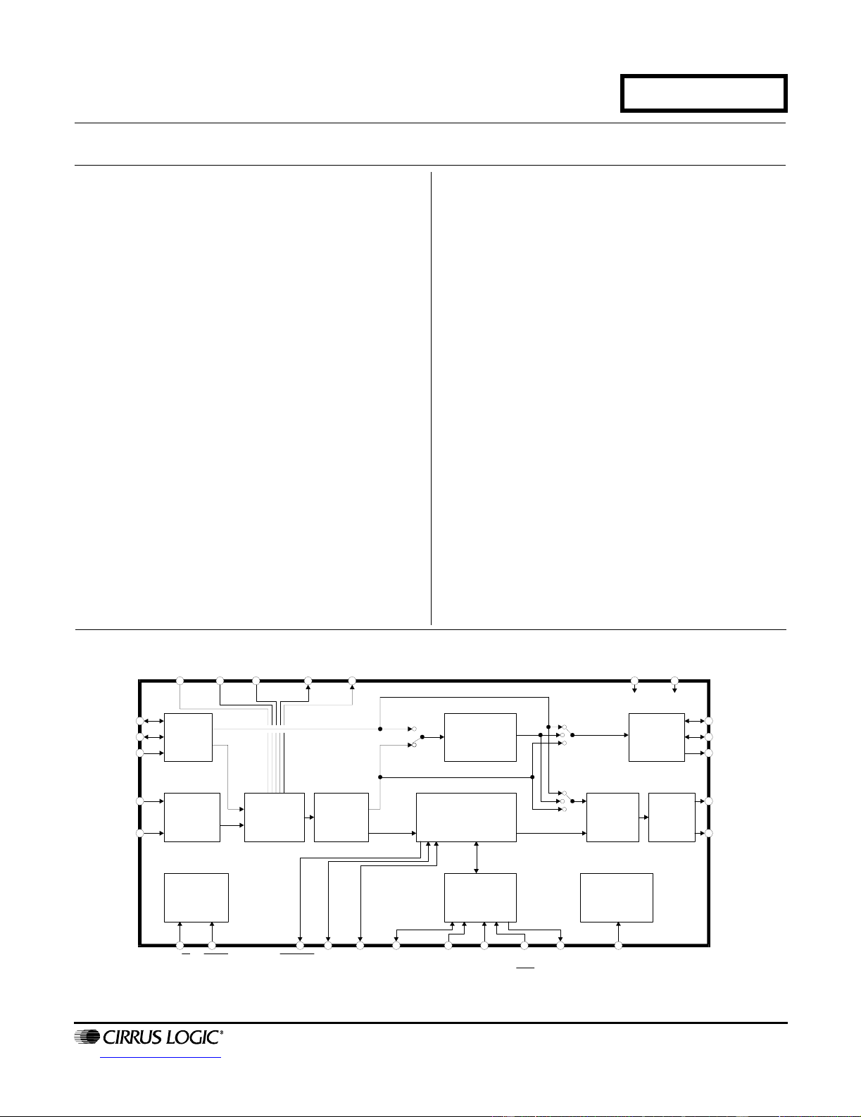
Serial
Audio
Input
Clock &
Data
Recovery
Misc.
Control
AES3
S/PDIF
Encoder
Serial
Audio
Output
Receiver AES3
S/PDIF
Decoder
Sample
Rate
Converter
C&Ubit
Data
Buffer
Control
Port &
Registers
Output
Clock
Generator
RXN
RXP
ILRCK
ISCLK
SDIN
OLRCK
OSCLK
SDOUT
TXP
TXN
RST OMCKEMPH U TCBL SDA/
CDOUT SCL/
CCLK AD1/
CDIN AD0/
CS INT
VA+ AGND FILT RERR VD+ DGND
H/S
RMCK
Driver
APRIL '07
DS245F4
CS8420
6DS245F4
CS8420
1. CHARACTERISTICS AND SPECIFICATIONS
All Min/Max characteristics and specifications are guaranteed over the Specified Operating Conditions. Typical
performance characteristics and specifications are derived from measurements taken at nominal supply voltages
and TA= 25°C.
SPECIFIED OPERATING CONDITIONS
AGND, DGND = 0 V, all voltages with respect to 0 V.
ABSOLUTE MAXIMUM RATINGS
AGND, DGND = 0 V; all voltages with respect to 0 V. Operation beyond these limits may result in permanent dam-
age to the device. Normal operation is not guaranteed at these extremes.
Notes:
1. Transient currents of up to 100 mA will not cause SCR latch-up.
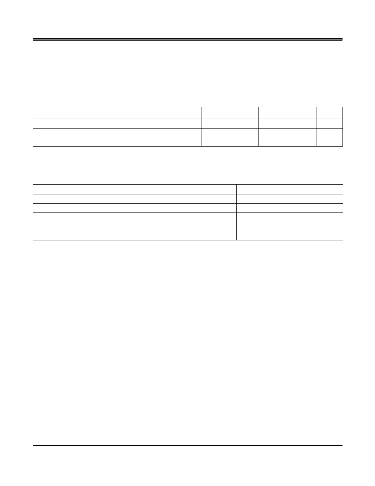
Parameter Symbol Min Typ Max Units
Power Supply Voltage VD+, VA+ 4.75 5.0 5.25 V
Ambient Operating Temperature: Commercial Grade
Automotive Grade TA-10
-40 -
-+70
+85 °C
°C
Parameter Symbol Min Max Units
Power Supply Voltage VD+, VA+ - 6.0 V
Input Current, Any Pin Except Supplies, RXP/RXN (Note 1) Iin -±10mA
Input Voltage Vin -0.3 (VD+) + 0.3 V
Ambient Operating Temperature (power applied) TA-55 125 °C
Storage Temperature Tstg -65 150 °C
DS245F4 7
CS8420
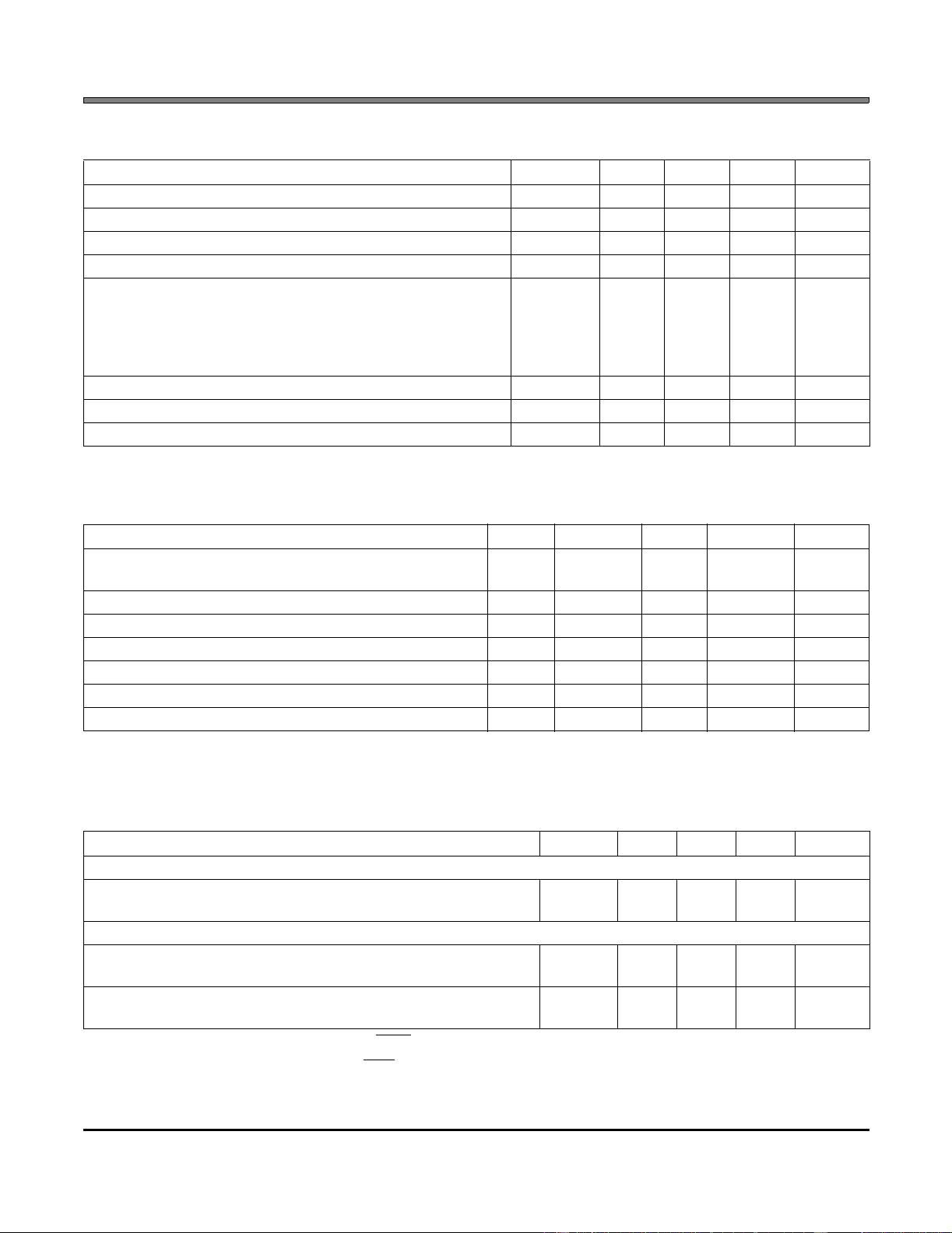
PERFORMANCE SPECIFICATIONS
DIGITAL FILTER CHARACTERISTICS
2. See “AES3 Transmitter and Receiver” on page 28.
DC ELECTRICAL SPECIFICATIONS
AGND = DGND = 0 V; all voltages with respect to 0 V.
3. Power Down Mode is defined as RST = LO with all clocks and data lines held static.
4. Normal operation is defined as RST = HI.
Parameter* Symbol Min Typ Max Units
Dynamic Range 120 128 - dB
Input Sample Rate (serial input port) Fsi 8 - 108 kHz
Output Sample Rate Fso 8 - 108 kHz
Output to Input Sample Rate Ratio 0.33 - 3
Total Harmonic Distortion + Noise
1 kHz, -1 dBFS, 0.33 < Fso/Fsi < 1.7
1 kHz, -1 dBFS, 0.33 < Fso/Fsi < 3
10 kHz, -1 dBFS, 0.33 < Fso/Fsi < 1.7
10 kHz, -1 dBFS, 0.33 < Fso/Fsi < 3
THD+N -
-
-
-
-
-
-
-
-117
-112
-110
-107
dB
dB
dB
dB
Peak idle channel noise component - - -140 dBFS
Resolution 16 - 24 bits
Gain Error -0.12 - 0 dB
Parameter* Symbol Min Typ Max Units
Passband Upsampling
Downsampling 0
0-
-0.4535*Fsi
0.4535*Fso Hz
Hz
Passband Ripple - - ±0.007 dB
Stopband (Downsampling) 0.5465*Fso - Fsi/2 Hz
Stopband Attenuation 110 - - dB
Group Delay (Note 2) tgd - - 1.75 ms
Group Delay Variation vs. Frequency Δtgd --0.0μs
Interchannel Phase Deviation - - 0.0 °
Parameters Symbol Min Typ Max Units
Power Down Mode (Note 3)
Supply Current in power down VA+
VD+ -
-20
20 -
-μA
μA
Normal Operation (Note 4)
Supply Current at 48 kHz Fso and Fsi VA+
VD+ -
-3.7
66 -
-mA
mA
Supply Current at 96 kHz Fso and Fsi VA+
VD+ -
-7.0
125 -
-mA
mA
8DS245F4
CS8420
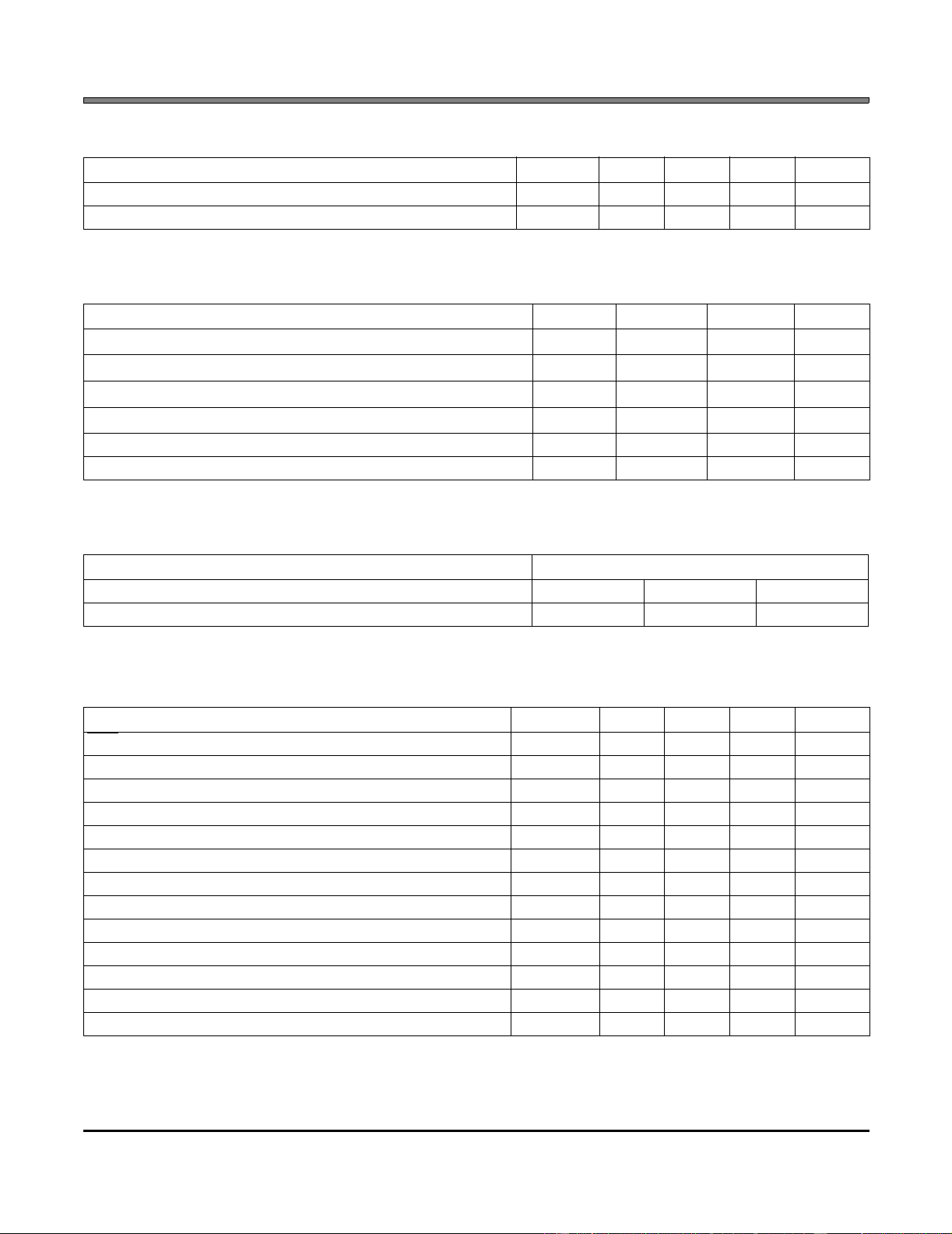
DIGITAL INPUT CHARACTERISTICS
DIGITAL INTERFACE SPECIFICATIONS
AGND = DGND = 0 V; all voltages with respect to 0 V.
TRANSMITTER CHARACTERISTICS
SWITCHING CHARACTERISTICS
Inputs: Logic 0 = 0 V, Logic 1 = VD+; CL= 20 pF.
5. Cycle-to-cycle jitter using 32-96 kHz external PLL components.
6. PLL is bypassed (RXD1:0 bits in the Clock Source Control register set to 10b), clock is input to the RMCK
pin.
Parameters Symbol Min Typ Max Units
Input Leakage Current Iin -±10±15μA
Differential Input Voltage, RXP to RXN VTH 200 - - mVpp
Parameters Symbol Min Max Units
High-Level Output Voltage (IOH = -3.2 mA), except TXP/TXN VOH (VD+) - 1.0 - V
Low-Level Output Voltage (IOH = 3.2 mA), except TXP/TXN VOL -0.4V
High-Level Output Voltage (IOH = -21 mA), TXP, TXN (VD+) - 0.7 - V
Low-Level Output Voltage (IOH = 21 mA), TXP, TXN - 0.7 V
High-Level Input Voltage, except RXP, RXN VIH 2.0 (VD+) + 0.3 V
Low-Level Input Voltage, except RXP, RXN VIL -0.3 0.8 V
Parameters Symbol Typ Units
TXP Output Resistance RTXP 25 Ω
TXN Output Resistance RTXN 25 Ω
Parameter Symbol Min Typ Max Units
RST pin Low Pulse Width 200 - - μs
OMCK Frequency for OMCK = 512 * Fso 4.096 - 55.3 MHz
OMCK Low and High Width for OMCK = 512 * Fso 8.2 - - ns
OMCK Frequency for OMCK = 384 * Fso 3.072 - 41.5 MHz
OMCK Low and High Width for OMCK = 384 * Fso 12.3 - - ns
OMCK Frequency for OMCK = 256 * Fso 2.048 - 27.7 MHz
OMCK Low and High Width for OMCK = 256 * Fso 16.4 - - ns
PLL Clock Recovery Sample Rate Range 8.0 - 108.0 kHz
RMCK output jitter (Note 5) -200-psRMS
RMCK output duty cycle 40 50 60 %
RMCK Input Frequency (Note 6) 2.048 - 27.7 MHz
RMCK Input Low and High Width (Note 6) 16.4 - - ns
AES3 Transmitter Output Jitter - - 1 ns

DS245F4 9
CS8420
SWITCHING CHARACTERISTICS - SERIAL AUDIO PORTS
Inputs: Logic 0 = 0 V, Logic 1 = VD+; CL= 20 pF.
7. The active edges of ISCLK and OSCLK are programmable.
8. When OSCLK, OLRCK, ISCLK, and ILRCK are derived from OMCK they are clocked from its rising edge.
When these signals are derived from RMCK, they are clocked from its falling edge.
9. The polarity of ILRCK and OLRCK is programmable.
10. No more than 128 SCLK per frame.
11. This delay is to prevent the previous I/OSCLK edge from being interpreted as the first one after I/OLRCK
has changed.
12. This setup time ensures that this I/OSCLK edge is interpreted as the first one after I/OLRCK has changed.
Parameter Symbol Min Typ Max Units
OSCLK Active Edge to SDOUT Output Valid (Note 7) tdpd - - 25 ns
SDIN Setup Time Before ISCLK Active Edge (Note 7) tds 20 - - ns
SDIN Hold Time After ISCLK Active Edge (Note 7) tdh 20 - - ns
Master Mode
O/RMCK to I/OSCLK active edge delay (Note 7, 8) tsmd 0 - 16 ns
O/RMCK to I/OLRCK delay (Note 9) tlmd 0 - 17 ns
I/OSCLK and I/OLRCK Duty Cycle - 50 - %
Slave Mode
I/OSCLK Period (Note 10) tsckw 36 - - ns
I/OSCLK Input Low Width tsckl 14 - - ns
I/OSCLK Input High Width tsckh 14 - - ns
I/OSCLK Active Edge to I/OLRCK Edge (Note 7, 9, 11) tlrckd 20 - - ns
I/OLRCK Edge Setup Before I/OSCLK Active Edge
(Note 7, 9, 12) tlrcks 20 - - ns
t
ILRCK
OLRCK
(input)
ISCLK
OSCLK
(input)
SDIN
SDOUT
tlrckd lrcks tsckh
tsckw
tsckl
tdpd
dh
t
ds
t
tsmd tlmd
Hardware Mode
Software Mode
ISCLK
OSCLK
(output)
ILRCK
OLRCK
(output)
RMCK
(output)
RMCK
(output)
OMCK
(input)
Figure 1. Audio Port Master Mode Timing Figure 2. Audio Port Slave Mode and Data Input Timing

10 DS245F4
CS8420
SWITCHING CHARACTERISTICS - CONTROL PORT - SPI™ MODE
Inputs: Logic 0 = 0 V, Logic 1 = VD+; CL= 20 pF.
13. If Fso or Fsi is lower than 46.875 kHz, the maximum CCLK frequency should be less than 128 Fso and
less than 128 Fsi. This is dictated by the timing requirements necessary to access the Channel Status and
User Bit buffer memory. Access to the control register file can be carried out at the full 6 MHz rate. The
minimum allowable input sample rate is 8 kHz, so choosing CCLK to be less than or equal to 1.024 MHz
should be safe for all possible conditions.
14. Data must be held for sufficient time to bridge the transition time of CCLK.
15. For fsck < 1 MHz.
Parameter Symbol Min Typ Max Units
CCLK Clock Frequency (Note 13) fsck 0-6.0MHz
CS High Time Between Transmissions tcsh 1.0 - - μs
CS Falling to CCLK Edge tcss 20 - - ns
CCLK Low Time tscl 66 - - ns
CCLK High Time tsch 66 - - ns
CDIN to CCLK Rising Setup Time tdsu 40 - - ns
CCLK Rising to DATA Hold Time (Note 14) tdh 18 - - ns
CCLK Falling to CDOUT Stable tpd - - 45 ns
Rise Time of CDOUT tr1 - - 25 ns
Fall Time of CDOUT tf1 - - 25 ns
Rise Time of CCLK and CDIN (Note 15) tr2 --100ns
Fall Time of CCLK and CDIN (Note 15) tf2 --100ns
tr2 tf2
tdsu tdh
tsch
tscl
CS
CCLK
CDIN
tcss
tpd
CDOUT
tcsh
Figure 3. SPI Mode Timing

DS245F4 11
CS8420
SWITCHING CHARACTERISTICS - CONTROL PORT - I²C®MODE
Inputs: Logic 0 = 0 V, Logic 1 = VD+; CL= 20 pF.
16. Data must be held for sufficient time to bridge the 25 ns transition time of SCL.
Parameter Symbol Min Typ Max Units
SCL Clock Frequency fscl - - 100 kHz
Bus Free Time Between Transmissions tbuf 4.7 - - μs
Start Condition Hold Time (prior to first clock pulse) thdst 4.0 - - μs
Clock Low Time tlow 4.7 - - μs
Clock High Time thigh 4.0 - - μs
Setup Time for Repeated Start Condition tsust 4.7 - - μs
SDA Hold Time from SCL Falling (Note 16) thdd 0--μs
SDA Setup Time to SCL Rising tsud 250 - - ns
Rise Time of Both SDA and SCL Lines tr- - 25 ns
Fall Time of Both SDA and SCL Lines tf- - 25 ns
Setup Time for Stop Condition tsusp 4.7 - - μs
tbuf thdst thdst
tlow tr
tf
thdd
thigh
tsud tsust
tsusp
Stop Start Start Stop
Repeated
SDA
SCL
Figure 4. I²C Mode Timing

12 DS245F4
CS8420
2. TYPICAL CONNECTION DIAGRAM
CS8420
Cable
Termination RXP
RXN
AES3/
SPDIF
Source
3-wire Serial
Audio Source ILRCK
ISCLK
SDIN
Clock Source
and Control RMCK
OMCK
Hardware
Control RST
RERR
EMPH
TCBL
To other
CS8420's
Cable
Interface AES3/
SPDIF
Equipment
TXP
TXN
3-wire Serial
Audio Input
Device
OLRCK
OSCLK
SDOUT
Microcontroller
SDA/CDOUT
AD0/CS
SCL/CCLK
AD1/CDIN
U
INT
VA+ VD+
Ferrite *
Bead
+5V
Analog
Supply *
+5V
Digital
Supply
0.1 Fμ
0.1 Fμ
* A separate analog supply is only necessary in applications where
RMCK is used for a jitter sensitive task. For applications where
RMCK is not used for a jitter sensitive task, connect VA+ to VD+
via a ferrite bead. Keep the decoupling capacitor between VA+
and AGND.
DGNDFILTAGND
RFILT
CFILT CRIP
H/S
47kΩ
/AD2
Figure 5. Recommended Connection Diagram for Software Mode

DS245F4 13
CS8420
3. GENERAL DESCRIPTION
The CS8420 is a fully asynchronous sample rate converter plus AES3 transceiver intended to be used in digital au-
dio systems. Such systems include digital mixing consoles, effects processors, tape recorders, and computer mul-
timedia systems. The CS8420 is intended for 16-, 20-, and 24-bit applications where the input sample rate is
unknown, or is known to be asynchronous to the system sample rate.
On the input side of the CS8420, AES3 or 3-wire serial format can be chosen. The output side produces both AES3
and 3-wire serial format. An I²C/SPI-compatible microcontroller interface allows full block processing of channel sta-
tus and user data via block reads from the incoming AES3 data stream and block writes to the outgoing AES3 data
stream. The user can also access information decoded from the input AES3 data stream, such as the presence of
non-audio data and pre-emphasis, as well as control the various modes of the device. For users who prefer not to
use a micro-controller, six hardware modes have been provided and documented towards the end of this datasheet.
In these modes, flexibility is limited, with pins providing some programmability.
When used for AES3-input/AES3-output applications, the CS8420 can automatically transceive user data that con-
forms to the IEC60958-recommended format. The CS8420 also allows access to the relevant bits in the AES3 data
stream to comply with the serial copy management system (SCMS).
The diagram on the cover of this data sheet shows the main functional blocks of the CS8420. Figure 5 shows the
supply and external connections to the device.
Familiarity with the AES3 and IEC60958 specifications are assumed throughout this document. Application Note 22:
Overview of Digital Audio Interface Data Structures, contains a tutorial on digital audio specifications. The paper An
Understanding and Implementation of the SCMS Serial Copy Management System for Digital Audio Transmission,
by Clif Sanchez, is an excellent tutorial on SCMS. It may be obtained from Cirrus Logic, Inc., or from the AES.
To guarantee system compliance, the proper standards documents should be obtained. The latest AES3 standard
should be obtained from the Audio Engineering Society (ANSI), the latest IEC60958 standard from the International
Electrotechnical Commission and the latest EIAJ CP-1201 standard from the Japanese Electronics Bureau.
14 DS245F4
CS8420
4. DATA I/O FLOW AND CLOCKING OPTIONS
The CS8420 can be configured for nine connectivity alternatives, referred to as data flows. Each data flow has an
associated clocking set-up. Figure 6 shows the data flow switching, along with the control register bits which control
the switches. This drawing only shows the audio data paths for simplicity. Figure 7 shows the internal clock routing
and the associated control register bits. The clock routing constraints determine which data routing options are ac-
tually usable.
Serial
Audio
Input
AES3
Encoder
Serial
Audio
Output
Receiver
Sample
Rate
Converter
RXP
RXN
ILRCK
ISCLK
SDIN
OLRCK
OSCLK
SDOU
T
TXP
TXN
AES3
TXOFFAESBP
SPD1-0
TXD1-0
SRCD
Figure 6. Software Mode Audio Data Flow Switching Options
SIMS
PLL
TXP
TXN
SDOUT
OSCLK
OLRCK
OMCKRMCK
RXP
ILRCK
ISCLK
SDIN
MUX
MUX
MUX
SWCLK
UNLOCK
01
0
1
01 CHANNEL
STATUS
MEMORY
USER
BIT
MEMORY
TRANSMIT
AES3
SERIAL
AUDIO
OUTPUT
INC
RXD0
MUX0
1OUTC
SERIAL
AUDIO
INPUT
RXD1
MUX
0
1
÷
CLK[1:0]
÷
RMCKF
SAMPLE
RATE
CONVERTER
Figure 7. CS8420 Clock Routing
*Note: When SWCLK mode is enabled, signal input on OMCK is only output through RMCK and not
routed back through the RXD1 multiplexer; RMCK is not bi-directional in this mode.

DS245F4 15
CS8420
The AESBP switch allows a TTL level, bi-phase mark-encoded data stream connected to RXP to be routed to the
TXP and TXN pin drivers. The TXOFF switch causes the TXP and TXN outputs to be driven to ground
In modes including the SRC function, there are two audio-data-related clock domains. One domain includes the in-
put side of SRC, plus the attached data source. The second domain includes the output side of the SRC, plus any
attached output ports.
There are two possible clock sources. The first known as the recovered clock, is the output of a PLL, and is con-
nected to the RCMK pin. The input to the PLL can be either the incoming AES3 data stream or the ILRCK word rate
clock from the serial audio input port. The second clock is input via the OMCK pin, and would normally be a crystal-
derived stable clock. The Clock Source Control Register bits determine which clock is connected to which domain.
By studying the following drawings, and appropriately setting the Data Flow Control and Clock Source Control reg-
ister bits, the CS8420 can be configured to fit a variety of application requirements.
The following drawings illustrate the possible valid data flows. The audio data flow is indicated by the thin lines; the
clock routing is indicated by the bold lines. The register settings for the Data Flow Control register and the Clock
Source Register are also shown for each data flow. Some of the register settings may appear to be not relevant to
the particular data flow in question, but have been assigned a particular state. This is done to minimize power con-
sumption. The AESBP data path from the RXP pin to the AES3 output drivers, and the TXOFF control, have been
omitted for clarity, but are present and functional in all modes where the AES3 transmitter is in use.
Figures 8and 9show audio data entering via the serial audio input port, then passing through the sample rate con-
verter, and then output both to the serial audio output port and to the AES3 transmitter. Figure 8 shows the PLL
recovering the input clock from ILRCK word clock. Figure 9 shows using a direct 256*Fsi clock input via the RMCK
pin, instead of the PLL.
Figure 10 shows audio data entering via the AES3 Receiver. The PLL locks onto the pre-ambles in the incoming
audio stream, and generates a 256*Fsi clock. The rate-converted data is then output via the serial audio output port
and via the AES3 transmitter.
Figure 11 shows the same data flow as Figure 8. The input clock is derived from an incoming AES3 data stream.
The incoming data must be synchronous to the AES3 data stream.
Figure 12 shows the same data flow as Figure 8. The input data must be synchronous to OMCK. The output data
is clocked by the recovered PLL clock from an AES3 input stream. This may be used to implement a “house sync”
architecture.
Figure 8 shows audio data entering via the AES3 receiver, passing through the sample rate converter, and then ex-
iting via the serial audio output port. Synchronous audio data may then be input via the serial audio input port and
output via the AES3 transmitter.
Figure 14 is the same as Figure 13, but without the sample rate converter. The whole data path is clocked via the
PLL generated recovered clock.
Figure 15 illustrates a standard AES3 receiver function, with no rate conversion.
Figure 16 shows a standard AES3 transmitter function, with no rate conversion.

16 DS245F4
CS8420
Figure 8. Serial Audio Input, using PLL, SRC Enabled Figure 9. Serial Audio Input, No PLL, SRC Enabled
Serial
Audio
Input AES3
Encoder
&Driver
Serial
Audio
Output
Sample
Rate
Converter
ILRCK
ISCLK
SDIN
OLRCK
OSCLK
SDOU
T
TXP
TXN
PLL
RMCK OMCK
TXD1-0:
SPD1-0:
SRCD:
OUTC:
INC:
RXD1-0:
00
00
0
0
0
00
Clock Source Control BitsData Flow Control Bits
Serial
Audio
Input AES3
Encoder
&Driver
Serial
Audio
Output
Sample
Rate
Converter
ILRCK
ISCLK
SDIN
OLRCK
OSCLK
SDOU
T
TXP
TXN
RMCK OMCK
TXD1-0:
SPD1-0:
SRCD:
OUTC:
INC:
RXD1-0:
00
00
0
0
0
1
0
Clock Source Control BitsData Flow Control Bits
AES3
Encoder
&Driver
Serial
Audio
Output
Sample
Rate
Converter
OLRCK
OSCLK
SDOU
T
TXP
TXN
PLL
RMCK OMCK
TXD1-0:
SPD1-0:
SRCD:
OUTC:
INC:
RXD1-0:
00
00
1
0
0
0
1
Clock Source Control BitsData Flow Control Bits
AES3
Rx &
Decode
RXP
RXN
Serial
Audio
Input AES3
Encoder
&Driver
Serial
Audio
Output
Sample
Rate
Converter
ILRCK
ISCLK
SDIN
OLRCK
OSCLK
SDOU
T
TXP
TXN
PLL
RMCK OMCK
TXD1-0:
SPD1-0:
SRCD:
OUTC:
INC:
RXD1-0:
00
00
0
0
0
0
1
Clock Source Control BitsData Flow Control Bits
AES3
Rx
RXP
RXN
Figure 10. AES3 Input, SRC Enabled Figure 11. Serial Audio Input, AES3 Input Clock Source,
Figure 12. Serial Audio Input, SRC Output Clocked by
AES3 Recovered Clock Figure 13. AES3 Input, SRC to Serial Audio Output,Serial
Audio Input to AES3 Out
AES3
Encoder
&Driver
Serial
Audio
Output
Sample
Rate
Converter
TXP
TX
N
PLL
RMCK OMCK
TXD1-0:
SPD1-0:
SRCD:
OUTC:
INC:
RXD1-0:
01
00
1
0
0
0
1
Clock Source Control BitsData Flow Control Bits
AES3
Rx &
Decode
RXP
RXN
Serial
Audio
Input
OLRCKOSCLKSDOUT ILR
C
K
ISCLKSDIN
Serial
Audio
Input
AES3
Encoder
&Driver
Serial
Audio
Output
Sample
Rate
Converter
ILRCK
ISCLK
SDIN OLRCK
OSCLK
SDOU
T
TXP
TXN
PLL
RMCKOMCK
TXD1-0:
SPD1-0:
SRCD:
OUTC:
INC:
RXD1-0:
00
00
0
1
1
0
1
Clock Source Control BitsData Flow Control Bits
AES3
Rx
RXP RXN
DS245F4 17
CS8420
Figure 14. AES3 Input to Serial Audio Output, Serial Au-
dio Input to AES3 Out, No SRC Figure 15. AES3 Input to Serial Audio Output Only
AES3
Encoder
&Driver
Serial
Audio
Output
OLRCKOSCLKSDOUT
TXP
TX
N
PLL
RMCK
TXD1-0:
SPD1-0:
SRCD:
OUTC:
INC:
RXD1-0:
01
10
0
1
0
0
1
Clock Source Control BitsData Flow Control Bits
AES3
Rx &
Decode
RXP
RXN
Serial
Audio
Input
ILRCK
ISCLKSDIN
Serial
Audio
Output
OLRCK
OSCLK
SDOU
T
PLL
RMCK
TXD1-0:
SPD1-0:
SRCD:
TXOFF:
OUTC:
INC:
RXD1-0:
10
10
0
1
1
0
01
Clock Source Control BitsData Flow Control Bits
AES3
Rx &
Decode
RXP
RXN
Serial
Audio
Input
AES3
Encoder
&Driver
ILRCK
ISCLK
SDIN TXP
TX
N
OMCK
TXD1-0:
SPD1-0:
SRCD:
OUTC:
INC:
RXD1-0:
01
01
0
0
1
00
Clock Source Control BitsData Flow Control Bits
Figure 16. Input Serial Port to AES3 Transmitter

18 DS245F4
CS8420
5. SAMPLE RATE CONVERTER (SRC)
Multirate digital signal processing techniques are used to conceptually upsample the incoming data to very high rate
and then downsample to the outgoing rate, resulting in a 24-bit output, regardless of the width of the input. The fil-
tering is designed so that a full input audio bandwidth of 20 kHz is preserved if the input sample and output sample
rates are greater than 44.1 kHz. When the output sample rate becomes less than the input sample rate, the input is
automatically band limited to avoid aliasing products in the output. Careful design ensures minimum ripple and dis-
tortion products are added to the incoming signal. The SRC also determines the ratio between the incoming and
outgoing sample rates, and sets the filter corner frequencies appropriately. Any jitter in the incoming signal has little
impact on the dynamic performance of the rate converter and has no influence on the output clock.
5.1 Dither
When using the AES3 input, and when using the serial audio input port in Left-Justified and I²S modes, all
input data is treated as 24 bits wide. Any truncation that has been done prior to the CS8420 to less than 24
bits should have been done using an appropriate dither process. If the serial audio input port is used to feed
the SRC, and the port is in Right-Justified mode, then the input data will be truncated to the SIRES bit setting
value. If SIRES bits are set to 16 or 20 bits, and the input data is 24 bits wide, truncation distortion will occur.
Similarly, in any serial audio input port mode, if an inadequate number of bit clocks are entered (say 16 in-
stead of 20), the input words will be truncated, causing truncation distortion at low levels. In summary, there
is no dithering mechanism on the input side of the CS8420, and care must be taken to ensure that no trun-
cation occurs.
Dithering is used internally where appropriate inside the SRC block.
The output side of the SRC can be set to 16, 20, or 24 bits. Optional dithering can be applied, and is auto-
matically scaled to the selected output word length. This dither is not correlated between left and right chan-
nels. It is recommended that the dither control bit be left in its default ON state.
5.2 SRC Locking, Varispeed and the Sample Rate Ratio Register
The SRC calculates the ratio between the input sample rate and the output sample rate and uses this infor-
mation to set up various parameters inside the SRC block. The SRC takes some time to make this calcula-
tion. For a worst case 3:1 to 1:3 input sample rate transition, the SRC will take 9400/Fso to settle (195 ms
at Fso of 48 kHz). For a power-up situation, the SRC will start from 1:1; the worst case time becomes
8300/Fso (172 ms at Fso of 48 kHz).
If the PLL is in use (either AES3 or serial input port), the worst case locking time for the PLL and the SRC
is the sum of each locking time.
If Fsi is changing, for example in a varispeed application, the REUNLOCK interrupt will occur, and the SRC
will track the incoming sample rate. During this tracking mode, the SRC will still rate convert the audio data,
but at increased distortion levels. Once the incoming sample rate is stable, the REUNLOCK interrupt will
become false, and the SRC will return to normal levels of audio quality.
The VFIFO interrupt occurs if the data buffer in the SRC overflows, which can occur if the input sample rate
changes at >10%/second.
Varispeed at Fsi slew rates approaching 10%/sec is only supported when the input is via the serial audio
input port. When using the AES3 input, high frame rate slew rates will cause the PLL to lose lock.
The sample rate ratio is also made available as a register, accessible via the control port. The upper 2 bits
of this register form the integer part of the ratio, while the lower6 bits formthe fractional part. Since, in many
instances Fso is known, this allows the calculation of the incoming sample rate by the host microcontroller.

DS245F4 19
CS8420
6. THREE-WIRE SERIAL AUDIO PORTS
A 3-wire serial audio input port and a 3-wire serial audio output port is provided. Each port can be adjusted to suit
the attached device via control registers. The following parameters are adjustable: master or slave, serial clock fre-
quency, audio data resolution, left or right justification of the data relative to left/right clock, optional 1-bit cell delay
of the 1st data bit, the polarity of the bit clock and the polarity of the left/right clock. By setting the appropriate control
bits, many formats are possible.
Figure 17 shows a selection of common input formats, along with the control bit settings. The clocking of the input
section of the CS8420 may be derived from the incoming ILRCK word rate clock, using the on-chip PLL. The PLL
operation is described in the AES receiver description on page 22. In the case of use with the serial audio input port,
the PLL locks onto the leading edges of the ILRCK clock.
Figure 18 shows a selection of common output formats, along with the control bit settings. A special AES3 direct
output format is included, which allows serial output port access to the V, U,and C bits embedded in the serial audio
data stream. The P bit is replaced by a bit indicating the location of the start of a block. This format is only available
when the serial audio output port is being clocked by the AES3 receiver-recovered clock. Also, the received-channel
status block start signal is only available in Hardware mode 5, as the RCBL pin.
In Master mode, the left/right clock and the serial bit clock are outputs, derived from the appropriate clock domain
master clock.
In Slave mode, the left/right clock and the serial bit clock are inputs. The left/right clock must be synchronous to the
appropriate master clock, but the serial bit clock can be asynchronous and discontinuous if required. By appropriate
phasing of the left/right clock and control of the serial clocks, multiple CS8420’s can share one serial port. The
left/right clock should be continuous, but the duty cycle does not have to be 50%, provided that enough serial clocks
are present in each phase to clock all the data bits. When in Slave mode, the serial audio output port must be set to
left-justified or I²S data.
When using the serial audio output port in Slave mode with an OLRCK input which is asynchronous to the port’s
data source, then an interrupt bit is provided to indicate when repeated or dropped samples occur.
The CS8420 allows immediate mute of the serial audio output port audio data via a control register bit.

20 DS245F4
CS8420
Figure 17. Serial Audio Input Example Formats
MSB LSB MSB LSB MSB
ILRCK
ISCLK
SDIN
Channel A Channel B
Left
Justified
(In)
ILRCK
ISCLK
MSB LSB MSB LSB
Channel A
SDIN MSB
Channel B
I²S
(In)
ILRCK
ISCLK
Channel A Channel B
MSB
SDIN MSB LSBLSB
Right
Justified
(In)
X = don’t care to match format, but does need to be set to the desired setting
+ I²S can accept an arbitrary number of bits, determined by the number of ISCLK cycles
* not 11 - See Serial Input Port Data Format Register Bit Descriptions for an explanation of the meaning of each bit
SIMS SISF SIRES1/0 SIJUST SIDEL SISPOL SILRPOL
Left-Justified X X 00 0 0 0 0
I²S XX00+0101
Right-Justified X X XX* 1 0 0 0

DS245F4 21
CS8420
Figure 18. Serial Audio Output Example Formats
X = don’t care to match format, but does need to be set to the desired setting
* not 11 - See Serial Output Data Format Register Bit Descriptions for an explanation of the meaning of each bit
SOMS SOSF SORES1/0 SOJUST SODEL SOSPOL SOLRPOL
Left-Justified X X XX* 0 0 0 0
I²S XXXX*0101
Right-Justified 1 X XX* 1 0 0 0
AES3DirectXX110000
OLRCK
OSCLK
SDOUT
Channel A Channel B
Left
Justified
(Out)
OLRCK
OSCLK
Channel A
SDOUT
Channel B
I²S
(Out)
OLRCK
OSCLK
Channel A Channel B
MSB
SDOUT MSB LSB
LSB
MSB Extended MSB Extended
Right
Justified
(Out)
OLRCK
OSCLK
Channel A Channel B
MSB
SDOUT LSB
LSB
Channel A Channel B
LSB
LSB MSB MSB MSB
AES3
Direct
(Out)
MSB MSB MSB
LSBLSB
MSB LSB MSB LSB MSB
CUVZCUVCUVCUV
Frame 191 Frame 0
Z

22 DS245F4
CS8420
7. AES3 TRANSMITTER AND RECEIVER
The CS8420 includes an AES3-type digital audio receiver and an AES3-type digital audio transmitter. A compre-
hensive buffering scheme provides read/write access to the channel status and user data. This buffering scheme is
described in “Channel Status and User Data Buffer Management” on page 81.
7.1 AES3 Receiver
The AES3 receiver accepts and decodes audio and digital data according to the AES3, IEC60958 (S/PDIF),
and EIAJ CP-1201 interface standards. The receiver consistsof a differential input stage, accessed viapins
RXP and RXN, a PLL based clock recovery circuit, and a decoder which separates the audio data from the
channel status and user data.
External components are used to terminate and isolate the incoming data cables from the CS8420. These
components are detailed in “External AES3/SPDIF/IEC60958 Transmitter and Receiver Components” on
page 78.
7.1.1 PLL, Jitter Attenuation, and Varispeed
Please see “PLL Filter” on page 87 for general description of the PLL,selectionof recommended PLLfilter
components, and layout considerations. Figure 5 shows the recommended configuration of the two ca-
pacitors and one resistor that comprise the PLL filter.
7.1.2 OMCK Out On RMCK
A special mode is available that allows the clock that is being input through the OMCK pin to be output
through the RMCK pin. This feature is controlled by the SWCLK bit in register 4 of the control registers.
When the PLL loses lock, the frequency of the VCO drops to 300 kHz. The SWCLK function allows the
clock from RMCK to be used as a clock in the system without any disruption when input is removed from
the Receiver.
7.1.3 Error Reporting and Hold Function
While decoding the incoming AES3 data stream, the CS8420 can identify several kinds of error, indicated
in the Receiver Error register. The UNLOCK bit indicates whether the PLL is locked to the incoming AES3
data. The V bit reflects the current validity bit status. The CONF (confidence) bit indicates the amplitude
of the eye pattern opening, indicating a link that is close to generating errors. The BIP (bi-phase) error bit
indicates an error in incoming bi-phase coding. The PAR (parity) bit indicates a received parity error.
The error bits are “sticky” - they are set on the first occurrence of the associated error and will remain set
until the user reads the register via the control port. This enables the register to log all unmasked errors
that occurred since the last time the register was read.
The Receiver Error Mask register allows masking of individual errors. The bits in this register serve as
masks for the corresponding bits of the Receiver Error Register. If a mask bit is set to 1, the error is con-
sidered unmasked, meaning that its occurrence will be reported in the receiver error register, will affect
the RERR pin, will invoke the occurrence of a RERR interrupt, and will affect the current audio sample
according to the status of the HOLD bits. The HOLD bits allow a choice of holding the previous sample,
replacing the current sample with zero (mute), or do not change the current audio sample. If a mask bit is
set to 0, the error is considered masked, meaning that its occurrence will not be reported in the receiver
error register, will not induce a pulse on RERR or generate a RERR interrupt, and will not affect the current
audio sample. The QCRC and CCRC errors do not affect the current audio sample, even if unmasked.

DS245F4 23
CS8420
7.1.4 Channel Status Data Handling
The first 2 bytes of the Channel Status block are decoded into the Receiver Channel Status register. The
setting of the CHS bit in the Channel Status Data Buffer Control register determines whether the channel
status decodes are from the A channel (CHS = 0) or B channel (CHS = 1).
The PRO (professional) bit is extracted directly. Also, for consumer data, the COPY (copyright) bit is ex-
tracted, and the category code and L bits are decoded to determine SCMS status, indicated by the ORIG
(original) bit. Finally, the AUDIO bit is extracted, and used to set an AUDIO indicator, as described in the
Non-Audio Auto Detection section below.
If 50/15 µs pre-emphasis is detected, then this is reflected in the state of the EMPH pin.
The encoded sample word length channel status bits are decoded according to AES3-1992 or IEC 60958.
If the AES3 receiver is the data source for the SRC, then the SRC audio input data is truncated according
to the channel status word length settings. Audio data routed to the serial audio output port is unaffected
by the word length settings; all 24 bits are passed on as received.
“Channel Status and User Data Buffer Management” on page 81 describes the overall handlingof CS and
U data.
7.1.5 User Data Handling
The incoming user data is buffered in a user-accessible buffer. Various automatic modes of re-transmit-
ting received U data are provided. “Channel Status and User Data Buffer Management” on page 81 de-
scribes the overall handling of CS and U data.
Received U data may also be output to the U pin, under the control of a control register bit. Depending on
the data flow and clocking options selected, there may not be a clock available to qualify the U data output.
Figure 19 illustrates the timing.
If the incoming user data bits have been encoded as Q-channel subcode, the data is decoded and pre-
sented in 10 consecutive registerlocations. An interrupt may be enabled to indicate the decoding of a new
Q-channel block, which may be read via the control port.
RCBL
out
VLRCK
C, U
Output
RCBL and C output are only available in hardware mode 5.
RCBL goes high 2 frames after receipt of a Z pre-amble, and is high for 16 frames.
VLRCK is a virtual word clock, which may not exist, but is used to illustrate the CU timing.
VLRCK duty cycle is 50%. VLRCK frequency is always equal to the incoming frame rate.
If no SRC is used, and the serial audio output port is in master mode, VLRCK = OLRCK.
If the serial audio output port is in slave mode, then VLRCK needs to be externally created, if required.
C, U transitions are ali
g
ned within 1% of VLRCK
p
eriod to VLRCK ed
g
es
±
Figure 19. AES3 Receiver Timing for C & U Pin Output Data

24 DS245F4
CS8420
7.1.6 Non-Audio Auto Detection
Since it is possible to convey non-audio data in an AES3 data stream, it is important to know whether the
incoming AES3 data stream is digital audio or other data. This information is typically conveyed in channel
status bit 1 (AUDIO), which is extracted automatically by the CS8420. However, certain non-audio sourc-
es, such as AC-3®or MPEG encoders, may not adhere to this convention, and the bit may not be properly
set. The CS8420 AES3 receiver can detect such non-audio data. This is accomplished by looking for a
96-bit sync code, consisting of 0x0000, 0x0000, 0x0000, 0x0000, 0xF872, and 0x4E1F. When the sync
code is detected, an internal AUTODETECT signal will be asserted. If no additional sync codes are de-
tected within the next 4096 frames, AUTODETECT will be de-asserted until another sync code is detect-
ed. The AUDIO bit in the Receiver Channel Status register is the logical OR of AUTODETECT and the
received channel status bit 1. If non-audio data is detected, the data is still processed exactly as if it were
normal audio. It is up to the user to mute the outputs as required.
7.2 AES3 Transmitter
The AES3 transmitter encodes and transmits audio and digital data according to the AES3, IEC60958
(S/PDIF), and EIAJ CP-1201 interface standards. Audio and control data are multiplexed together and
bi-phase mark-encoded. The resulting bit stream is then driven directly, or through a transformer, to an
output connector.
The transmitter is usually clocked from the output side clock domain of the sample rate converter. This
clock may be derived from the clock input pin OMCK, or from the incoming data. In data flows with no
SRC, and where OMCK is asynchronous to the data source, an interrupt bit is provided that will go high
every time a data sample is dropped or repeated.
The channel status (C) and user channel (U) bits in the transmitted data stream are taken from storage
areas within the CS8420. The user can manipulate the contents of the internal storage with a microcon-
troller. The CS8420 will also run inone of severalautomatic modes. “ChannelStatus and User Data Buffer
Management”on page 81provides detailed descriptions of each automaticmode, anddescribesmethods
for accessing the storage areas. The transmitted user data can optionally be input via the U pin, under the
control of a control port register bit. Figure 20 shows the timing requirements for inputting U data via the
U pin.
7.2.1 Transmitted Frame and Channel Status Boundary Timing
The TCBL pin may be an input or an output, and is used tocontrol or indicate the start of transmitted chan-
nel status block boundaries.
In some applications, it may be necessary to control the precise timing of the transmitted AES3 frame
boundaries. This may be achieved in 3 ways:
1) With TCBL configured as an input, and TCBL transitions high for >3 OMCK clocks, it will cause a frame
start, and a new channel status block start.
2) If the AES3 output comes from the AES3 input, while there isno SRC, setting TCBL as output willcause
AES3 output frame boundaries to align with AES3 input frame boundaries.
3) If the AES3 output comes from the serial audio input port while the port is in Slave mode, and TCBL is
set to output, then the start of the A channel sub-frame will be aligned with the leading edge of ILRCK.
Table of contents
Other Cirrus Logic Media Converter manuals


Popular Media Converter manuals by other brands


HEIDENHAIN
HEIDENHAIN AK ECA 4410 operating instructions

Transition Networks
Transition Networks E-CX-FRL-03 installation guide

Siko
Siko AH3650M quick start guide

Lika
Lika ROTAPULS I58 Series manual

Analytic Systems
Analytic Systems VTC600 Series Operation manual

GRASS VALLEY
GRASS VALLEY 8960ENC - datasheet


