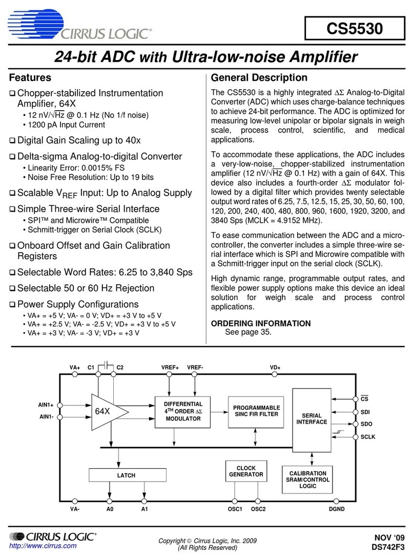
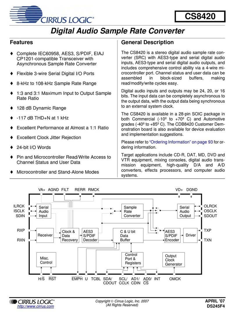
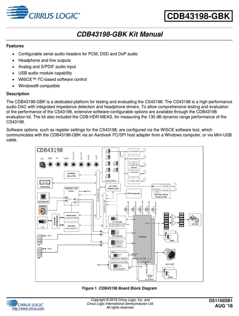
Cirrus Logic CS5460A User manual

Preliminary Product Information This document contains information for a new product.
Cirrus Logic reserves the right to modify this product without notice.
1
Copyright Cirrus Logic, Inc. 2001
(All Rights Reserved)
P.O. Box 17847, Austin, Texas 78760
(512) 445 7222 FAX: (512) 445 7581
http://www.cirrus.com
CS5460A
Single Phase Bi-Directional Power/Energy IC
Features
!Energy Data Linearity: ±0.1% of Reading
over 1000:1 Dynamic Range.
!On-Chip Functions: (Real) Energy, I ∗V,
IRMS and VRMS, Energy-to-Pulse Conversion
!Smart “Auto-Boot” Mode from Serial
EEPROM Enables Use without MCU.
!AC or DC System Calibration
!Mechanical Counter/Stepper Motor Driver
!Meets Accuracy Spec for IEC 687/1036, JIS
!Power Consumption <12 mW
!Interface Optimized for Shunt Sensor
!V vs. I Phase Compensation
!Ground-Referenced Signals with Single
Supply
!On-chip 2.5 V Reference (MAX 60 ppm/°C
drift)
!Simple Three-Wire Digital Serial Interface
!Watch Dog Timer
!Power Supply Monitor
!Power Supply Configurations
VA+ = +5 V; VA- = 0 V; VD+ = +3.3 V to +5 V
Description
The CS5460A is a highly integrated ∆Σ Analog-to-Digital
Converter (ADC) which combines two ∆Σ ADCs, high
speed power calculation functions, and a serial interface
on a single chip. It is designed to accurately measure
and calculate: Real (True) Energy, Instantaneous Pow-
er, IRMS,andV
RMS forsinglephase2-or3-wirepower
metering applications. The CS5460A interfaces to a
low-cost shunt resistor or transformer to measure cur-
rent, and resistive divider or potential transformer to
measure voltage. The CS5460A features a bi-directional
serial interface for communication with a micro-control-
ler and a pulse output engine for which the average
pulse frequency is proportional to the real power.
CS5460A has on-chip functionality to facilitate AC or DC
system-level calibration.
The “Auto-Boot” feature allows the CS5460A to function
‘stand-alone’ and to initialize itself on system power-up.
In Auto-Boot Mode, the CS5460A reads the calibration
data and start-up instructions from an external EE-
PROM. In this mode, the CS5460A can operate without
a microcontroller, in order to lower the total bill-of-mate-
rials cost, when the meter is intended for use in
high-volume/residential metering applications.
ORDERING INFORMATION:
CS5460A-BS -40°Cto+85°C 24-pin SSOP
PGA
x10,x50
VA+ VD+
IIN+
IIN-
VIN+
VIN-
VREFIN
VREFOUT
VA- XIN XOUT CPUCLK DGND
CS
SDO
SDI
SCLK
INT
EOUT
Digital
Filter
High Pass
Filter
Voltage
Reference System
Clock /K Clock
Generator
Serial
Interface
Power
Calculation
Engine
(Energy
I*V
I,V )
RMS RMS
Energy-to-
Pulse
Converter
Power
Monitor
PFMON
x1
x10
4Order
πΓ
Modulator
th
RESET
Digital
Filter
Calibration
SRAM
EDIR
High Pass
Filter
2Order
πΓ
Modulator
nd
Watch Dog
Timer
MODE
Control /
OCT ‘01
DS284PP4

CS5460A
2DS284PP4
TABLE OF CONTENTS
1. CHARACTERISTICS AND SPECIFICATIONS ........................................................................5
ANALOG CHARACTERISTICS................................................................................................5
VREFOUT REFERENCE OUTPUT VOLTAGE........................................................................7
3.3 V DIGITAL CHARACTERISTICS........................................................................................8
ABSOLUTE MAXIMUM RATINGS ...........................................................................................8
SWITCHING CHARACTERISTICS ..........................................................................................9
2. GENERAL DESCRIPTION .....................................................................................................12
2.1 Theory of Operation .........................................................................................................12
2.1.1 DS Modulators ...................................................................................................12
2.1.2 High-Rate Digital Low-Pass Filters .....................................................................12
2.1.3 Digital Compensation Filters ...............................................................................13
2.1.4 Digital High-Pass Filters ......................................................................................13
2.1.5 Overall Filter Response .......................................................................................13
2.1.6 Gain and DC Offset Adjustment ..........................................................................13
2.1.7 Real Energy and RMS Computations .................................................................13
2.2 Performing Measurements ...............................................................................................13
2.2.1 CS5460A Linearity Performance .........................................................................15
2.2.2 Single Computation Cycle (C=0) .........................................................................16
2.2.3 Continuous Computation Cycles (C=1) ...............................................................16
2.3 Basic Application Circuit Configurations ..........................................................................17
3. SERIAL PORT OVERVIEW ....................................................................................................18
3.1 Commands (Write Only) ..................................................................................................20
3.2 Serial Port Interface .........................................................................................................23
3.3 Serial Read and Write ......................................................................................................23
3.3.1 Register Write .....................................................................................................23
3.3.2 Register Read .....................................................................................................23
3.4 System Initialization .........................................................................................................24
3.5 Serial Port Initialization ....................................................................................................24
3.6 CS5460A Power States ...................................................................................................25
4. FUNCTIONAL DESCRIPTION ...............................................................................................26
4.1 Pulse-Rate Output ...........................................................................................................26
4.2 Pulse Output for Normal, Stepper Motor and Mechanical Counter Format .....................28
4.2.1 Normal Format ....................................................................................................28
4.2.2 Mechanical Counter Format ................................................................................29
4.2.3 Stepper Motor Format .........................................................................................29
4.3 Auto-Boot Mode Using EEPROM ....................................................................................30
4.3.1 Auto-Boot Configuration ......................................................................................30
4.3.2 Auto-Boot Data for EEPROM ..............................................................................30
Contacting Cirrus Logic Support
For a complete listing of Direct Sales, Distributor, and Sales Representative contacts, visit the Cirrus Logic web site at:
http://www.cirrus.com/corporate/contacts/sales/cfm
Microwire is a trademark of National Semiconductor Corporation.
Preliminary product information describes products which are in production, but for which full characterization data is not yet available. Advance product infor-
mation describes products which are in development and subject to development changes. Cirrus Logic, Inc. has made best efforts to ensure that the information
contained in this document is accurate and reliable. However, the information is subject to change without notice and is provided “AS IS” without warranty of
any kind (express or implied). No responsibility is assumed by Cirrus Logic, Inc. for the use of this information, nor for infringements of patents or other rights
of third parties. This document is the property of Cirrus Logic, Inc. and implies no license under patents, copyrights, trademarks, or trade secrets. No part of
this publication may be copied, reproduced, stored in a retrieval system, or transmitted, in any form or by any means (electronic, mechanical, photographic, or
otherwise) without the prior written consent of Cirrus Logic, Inc. Items from any Cirrus Logic website or disk may be printed for use by the user. However, no
part of the printout or electronic files may be copied, reproduced, stored in a retrieval system, or transmitted, in any form or by any means (electronic, mechanical,
photographic, or otherwise) without the prior written consent of Cirrus Logic, Inc. Furthermore, no part of this publication may be used as a basis for manufacture
or sale of any items without the prior written consent of Cirrus Logic, Inc. The names of products of Cirrus Logic, Inc. or other vendors and suppliers appearing
in this document may be trademarks or service marks of their respective owners which may be registered in some jurisdictions. A list of Cirrus Logic, Inc. trade-
marks and service marks can be found at http://www.cirrus.com.

CS5460A
DS284PP4 3
4.3.3 Which EEPROMs Can Be Used? ....................................................................... 31
4.4 Interrupt and Watchdog Timer ......................................................................................... 33
4.4.1 Interrupt ............................................................................................................... 33
4.4.1.1 Clearing the Status Register ............................................................... 33
4.4.1.2 Typical use of the INT pin ................................................................... 33
4.4.1.3 INT Active State .................................................................................. 34
4.4.1.4 Exceptions .......................................................................................... 34
4.4.2 Watch Dog Timer ................................................................................................ 34
4.5 Oscillator Characteristics ................................................................................................. 34
4.6 Analog Inputs ................................................................................................................... 35
4.7 Voltage Reference ........................................................................................................... 35
4.8 Calibration ....................................................................................................................... 36
4.8.1 Overview of Calibration Process ......................................................................... 36
4.8.2 The Calibration Registers ................................................................................... 37
4.8.3 Calibration Sequence .......................................................................................... 37
4.8.4 Calibration Signal Input Level ............................................................................. 38
4.8.5 Calibration Signal Frequency .............................................................................. 38
4.8.6 Input Configurations for Calibrations ................................................................... 38
4.8.7 Description of Calibration Algorithms .................................................................. 39
4.8.7.1 AC Offset Calibration Sequence ......................................................... 39
4.8.7.2 DC Offset Calibration Sequence ......................................................... 40
4.8.7.3 AC Gain Calibration Sequence ........................................................... 40
4.8.7.4 DC Gain Calibration Sequence .......................................................... 40
4.8.8 Duration of Calibration Sequence ....................................................................... 41
4.8.9 Is Calibration Required? ............................................................................. 41
4.8.10 Order of Calibration Sequences ........................................................................ 42
4.8.11 Calibration Tips ................................................................................................. 43
4.9 Phase Compensation ...................................................................................................... 43
4.10 Time-Base Calibration Register ..................................................................................... 44
4.11 Power Offset Register ................................................................................................... 44
4.12 Input Protection - Current Limit ...................................................................................... 45
4.13 Input Filtering ................................................................................................................. 46
4.14 Protection Against High-Voltage and/or High-Current Surges ...................................... 50
4.15 Improving RFI Immunity ................................................................................................ 50
4.16 PCB Layout ...................................................................................................................52
5. REGISTER DESCRIPTION ................................................................................................... 53
5.1 Configuration Register...................................................................................................... 53
5.2 Current Channel DC Offset Register and Voltage Channel DC Offset Register .............. 55
5.3 Current Channel Gain Register and Voltage Channel Gain Register............................... 55
5.4 Cycle Count Register........................................................................................................ 55
5.5 Pulse-Rate Register ......................................................................................................... 56
5.6 I,V,P,E Signed Output Register Results........................................................................... 56
5.7 IRMS, VRMS Unsigned Output Register Results............................................................. 56
5.8 Timebase Calibration Register ......................................................................................... 56
5.9 Power Offset Register ...................................................................................................... 57
5.10 Current Channel AC Offset Register and Voltage Channel AC Offset Register............. 57
5.11 Status Register and Mask Register................................................................................ 57
5.12 Control Register.............................................................................................................. 59
6. PIN DESCRIPTION ................................................................................................................. 60
7. PACKAGE DIMENSIONS ...................................................................................................... 62

CS5460A
4DS284PP4
LIST OF FIGURES
Figure 1. CS5460A Read and Write Timing Diagrams..................................................................10
Figure 2. CS5460A Auto-Boot Sequence Timing..........................................................................11
Figure 3. Data Flow.......................................................................................................................14
Figure 4. Voltage Input Filter Characteristics................................................................................14
Figure 5. Current Input Filter Characteristics ................................................................................14
Figure 6. Typical Connection Diagram (One-Phase 2-Wire, Direct Connect to Power Line)........18
Figure 7. Typical Connection Diagram (One-Phase 2-Wire, Isolated from Power Line)...............18
Figure 8. Typical Connection Diagram (One-Phase 3-Wire).........................................................19
Figure 9. Typical Connection Diagram (One-Phase 3-Wire - No Neutral Available).....................19
Figure 10. Time-plot representation of pulse output for a typical burst of pulses (Normal Format)28
Figure 11. Mechanical Counter Format on EOUT and EDIR ........................................................29
Figure 12. Stepper Motor Format on EOUT and EDIR .................................................................29
Figure 13. Typical Interface of EEPROM to CS5460A..................................................................30
Figure 14. Timing Diagram for Auto-Boot Sequence ....................................................................31
Figure 15. CS5460A Auto-Boot Configuration: Automatic Restart After Power Failure................33
Figure 16. Oscillator Connection...................................................................................................35
Figure 17. VREFOUT Voltage vs. Temperature characteristic for a typical CS5460A sample.....35
Figure 18. System Calibration of Gain. .........................................................................................39
Figure 19. System Calibration of Offset. .......................................................................................39
Figure 20. Calibration Data Flow...................................................................................................40
Figure 21. Example of AC Gain Calibration ..................................................................................41
Figure 22. Another Example of AC Gain Calibration.....................................................................41
Figure 23. Example of DC Gain Calibration ..................................................................................41
Figure 24. Input Protection for Single-Ended Input Configurations...............................................51
Figure 25. CS5460A Register Diagram.........................................................................................53
LIST OF TABLES
Table 1. Differential Input Voltage vs. Output Code ............................................................................15
Table 2. Available range of ±0.1% output linearity, with default settings in the gain/offset registers...15
Table 3. Default Register Values upon Reset Event ...........................................................................24

CS5460A
DS284PP4 5
1. CHARACTERISTICS AND SPECIFICATIONS
ANALOG CHARACTERISTICS (TA=-40°Cto+85°C;VA+=VD+=+5V±10%;VREFIN=+2.5V;
VA- = AGND = 0 V; MCLK = 4.096 MHz, K = 1; N = 4000 ==> OWR = 4000 Sps.)(See Notes 1, 2, 3, 4, and 5.)
Notes: 1. Bipolar Offset Errors and Full-Scale Gain Errors for the current and voltage channels refer to the
respective Irms Register and Vrms Register output, when the device is operating in ‘continuous
computation cycles’ data acquisition mode, after offset/gain system calibration sequences have been
executed. These specs do not apply to the error of the Instantaneous Current/Voltage Register output.
2. Specifications guaranteed by design, characterization, and/or test.
3. Analog signals are relative to VA- and digital signals to DGND unless otherwise noted.
4. In requiring VA+=VD+=5V ±10%, note that it is allowable for VA+, VD+ to differ by as much as ±200mV,
as long as VA+ > VD+.
5. Note that “Sps” is an abbreviation for units of “samples per second”.
6. Effective Input Impedance (Zin) is determined by clock frequency (DCLK) and Input Capacitance (IC).
Zin = 1/(IC*DCLK/4). Note that DCLK = MCLK / K.
Parameter Symbol Min Typ Max Unit
Accuracy (Both Channels)
Common Mode Rejection (DC, 50, 60 Hz) CMRR 80 - - dB
Offset Drift (Without the High Pass Filter) - 5 - nV/°C
Analog Inputs (Current Channel)
Maximum Differential Input Voltage Range (Gain = 10)
{(VIIN+)-(VIIN-)} (Gain = 50) IIN -
-±250
±50 -
-mV
mV
Total Harmonic Distortion THDI74 - - dB
Common Mode + Signal on IIN+ or IIN- (Gain = 10 or 50) -0.25 - VA+ V
Crosstalk with Voltage Channel at Full Scale (50, 60 Hz) - - -115 dB
Input Capacitance (Gain = 10)
(Gain = 50) Cin -
-25
25 -
-pF
pF
Effective Input Impedance (Note 6)
(Gain = 10)
(Gain = 50) ZinI
ZinI -
-30
30 -
-kΩ
kΩ
Noise (Referred to Input) (Gain = 10)
(Gain = 50) -
--
-20
4µVrms
µVrms
Accuracy (Current Channel)
Bipolar Offset Error (Note 1) VOSI- ±0.001 - %F.S.
Full-Scale Error (Note 1) FSEI- ±0.001 - %F.S.
Analog Inputs (Voltage Channel)
Maximum Differential Input Voltage Range {(VVIN+)-(VVIN-)} VIN -±250-mV
Total Harmonic Distortion THDV62 - - dB
Common Mode + Signal on VIN+ or VIN- -0.25 - VA+ V
Crosstalk with Current Channel at Full Scale (50, 60 Hz) - - -70 dB
Input Capacitance CinV -0.2-pF
Effective Input Impedance (Note 6) ZinV -5-MΩ
Noise(ReferredtoInput) - - 250 µV
rms
Accuracy (Voltage Channel)
Bipolar Offset Error (Note 1) VOSV- ±0.01 - %F.S.
Full-Scale Error (Note 1) FSEV- ±0.01 - %F.S.

CS5460A
6DS284PP4
ANALOG CHARACTERISTICS (Continued)
Notes: 7. The minimum FSCR is limited by the maximum allowed gain register value.
8. All outputs unloaded. All inputs CMOS level.
9. Definition for PSRR: VREFIN tied to VREFOUT, VA+ = VD+ = 5V, a 150mV zero-to-peak sinewave
(frequency = 60Hz) is imposed onto the +5V supply voltage at VA+ and VD+ pins. The “+” and “-” input
pins of both input channels are shorted to VA-. Then the CS5460A is commanded to ’continuous
computation cycles’ data acquisition mode, and digital output data is collected for the channel under
test. The zero-peak value of the digital sinusoidal output signal is determined, and this value is
converted into the zero-peak value of the sinusoidal voltage that would need to be applied at the
channel’s inputs, in order to cause the same digital sinusoidal output. This voltage is then defined as
Veq. PSRR is then (in dB):
10. When voltage level on PFMON is sagging, and LSD bit is at 0, the voltage at which LSD bit is set to 1.
11. Assuming that the LSD bit has been set to 1 (because PFMON voltage fell below PMLO), then if/when
the PFMON voltage starts to rise again, PMHI is the voltage level (on PFMON pin) at which the LSD bit
can be permanently reset back to 0 (without instantaneously changing back to 1). Attempts (by the
user) to reset the LSD bit before this condition is true will not be successful. This condition indicates
that power has been restored. Typically, for a given sample, the PMHI voltage will be ~100mV above
the PMLO voltage.
Parameter Symbol Min Typ Max Unit
Dynamic Characteristics
Phase Compensation Range (Voltage Channel, 60 Hz) -2.4 - +2.5 °
High Rate Filter Output Word Rate (Both Channels) OWR - DCLK/1024 - Sps
Input Sample Rate DCLK = MCLK/K - DCLK/8 - Sps
Full Scale DC Calibration Range (Note 7) FSCR 25 - 100 %F.S.
Channel-to-Channel Time-Shift Error
(when PC[6:0] bits are set to “0000000”) 1.0 µs
High Pass Filter Pole Frequency -3 dB - 0.5 - Hz
Power Supplies
Power Supply Currents (Active State) IA+
ID+ (VD+ = 5 V)
ID+ (VD+=3.3V)
PSCA
PSCD
PSCD
-
-
-
1.3
2.9
1.7
-
-
-
mA
mA
mA
Power Consumption Active State (VD+ = 5 V)
(Note8) ActiveState(VD+=3.3V)
Stand-By State
Sleep State
PC -
-
-
-
21
11.6
6.75
10
25
-
-
-
mW
mW
mW
µW
Power Supply Rejection Ratio (50, 60 Hz)
for Current Channel (Gain = 10)
(Note 9) (Gain = 50) PSRR
PSRR 56
70 -
--
-dB
dB
Power Supply Rejection Ratio (50, 60 Hz)
for Voltage Channel (Note 9) PSRR 50 - - dB
PFMON Power-Fail Detect Threshold (Note 10) PMLO 2.3 2.45 - V
PFMON “Power-Restored” Detect Threshold (Note 11) PMHI - 2.55 2.7 V
PSRR 20 0.150V
Veq
------------------
log⋅=

CS5460A
DS284PP4 7
VREFOUT REFERENCE OUTPUT VOLTAGE
Notes: 12. See Section 4.7 for definition of VREFOUT Temperature Coefficient spec.
5V DIGITAL CHARACTERISTICS (TA= -40° C to +85° C; VA+ = VD+ = 5 V ±10% VA-, DGND =
0 V) (See Notes 3, 4, and 13)
13. Notethat the 5V characteristicsareguaranteed by characterization. Only themorerigorous3.3Vdigital
characteristics are actually verified during production test.
14. Applies to all INPUT pins except XIN pin (leakage current < 50 µA) and MODE pin (leakage current <
25 µA).
Parameter Symbol Min Typ Max Unit
Reference Output
Output Voltage REFOUT +2.4 - +2.6 V
VREFOUT Temperature Coefficient (Note 12) TVREFOUT - 25 - ppm/°C
Load Regulation (Output Current 1 µA Source or Sink) ∆VR-610mV
Reference Input
Input Voltage Range VREFIN +2.4 +2.5 +2.6 V
Input Capacitance - 4 - pF
Input CVF Current - 25 - nA
Parameter Symbol Min Typ Max Unit
High-Level Input Voltage
All Pins Except XIN, SCLK and RESET
XIN
SCLK and RESET
VIH 0.6 VD+
(VD+)-0.5
0.8 VD+
-
-
-
-
-
-
V
V
V
Low-Level Input Voltage
All Pins Except XIN, SCLK, and RESET
XIN
SCLK and RESET
VIL -
-
-
-
-
-
0.8
1.5
0.2 VD+
V
V
V
High-Level Output Voltage (except XOUT) Iout =+5mA V
OH (VD+)-1.0 - - V
Low-Level Output Voltage (except XOUT) Iout =-5mA V
OL --0.4V
Input Leakage Current (Note 14) Iin -±1±10µA
3-State Leakage Current IOZ --±10µA
Digital Output Pin Capacitance Cout -5-pF

CS5460A
8DS284PP4
3.3 V DIGITAL CHARACTERISTICS (TA= -40°Cto+85°C;VA+=5V±10%,VD+=3.3V±10%;
VA-, DGND = 0 V) (See Notes 3, 4, and 13)
Notes: 15. All measurements performed under static conditions.
16. If VD+ = 3V and if XIN input is generated using crystal, then XIN frequency must remain between 2.5
MHz - 5.0 MHz. If using oscillator, full XIN frequency range is available, see Switching Characteristics.
ABSOLUTE MAXIMUM RATINGS (DGND = 0 V; See Note 17) WARNING: Operation at or beyond
these limits may result in permanent damage to the device. Normal operation is not guaranteed at these extremes.
Notes: 17. All voltages with respect to ground.
18. VA+ and VA- must satisfy {(VA+) - (VA-)} ≤+6.0 V.
19. VD+ and VA- must satisfy {(VD+) - (VA-)} ≤+6.0 V.
20. Applies to all pins including continuous over-voltage conditions at the analog input (AIN) pins.
21. Transient current of up to 100 mA will not cause SCR latch-up.
22. Maximum DC input current for a power supply pin is ±50 mA.
23. Total power dissipation, including all input currents and output currents.
Parameter Symbol Min Typ Max Unit
High-Level Input Voltage
All Pins Except XIN, XOUT, SCLK, and RESET
XIN
SCLK and RESET
VIH 0.6 VD+
(VD+)-0.5
0.8 VD+
-
-
-
-
-
-
V
V
V
Low-Level Input Voltage
AllPinsExceptXIN,XOUT,SCLK,andRESET
XIN
SCLK and RESET
VIL -
-
-
-
-
-
0.48
0.3
0.2 VD+
V
V
V
High-Level Output Voltage (except XIN, XOUT)Iout =+5mA V
OH (VD+)-1.0 - - V
Low-Level Output Voltage (except XIN, XOUT) Iout =-5mA V
OL --0.4V
Input Leakage Current (Note 14) Iin -±1±10µA
3-State Leakage Current IOZ --±10µA
Digital Output Pin Capacitance Cout -5-pF
Parameter Symbol Min Typ Max Unit
DC Power Supplies (Notes 18 and 19)
Positive Digital
Positive Analog
Negative Analog
VD+
VA+
VA-
-0.3
-0.3
+0.3
-
-
-
+6.0
+6.0
-6.0
V
V
V
Input Current, Any Pin Except Supplies(Note 20, 21, and 22) IIN --±10mA
Output Current IOUT --±25mA
Power Dissipation (Note 23) PD--500mW
Analog Input Voltage All Analog Pins VINA (VA-)-0.3 - (VA+)+0.3 V
Digital Input Voltage All Digital Pins VIND DGND - 0.3 - (VD+) + 0.3 V
Ambient Operating Temperature TA-40 - 85 °C
Storage Temperature Tstg -65 - 150 °C

CS5460A
DS284PP4 9
SWITCHING CHARACTERISTICS (TA= -40° C to +85 °C; VA+ = 5.0 V ±10%; VD+ = 3.0 V ±10%
or 5.0 V ±10%; VA- = 0.0 V; Logic Levels: Logic 0 = 0.0 V, Logic 1 = VD+; CL = 50 pF))
Notes: 24. Device parameters are specified with a 4.096 MHz clock, however, clocks between 3 MHz to 20 MHz
can be used. However, for input frequencies over 5 MHz, an external oscillator must be used, or if a
crystal over 5 MHz is to be used, then VD+ must be set to 5V (not 3V).
25. If external MCLK is used, then duty cycle must be between 45% and 55% to maintain this specification.
26. Specified using 10% and 90% points on wave-form of interest. Output loaded with 50 pF.
27. Oscillator start-up time varies with crystal parameters. This specification does not apply when using an
external clock source.
Parameter Symbol Min Typ Max Unit
Master Clock FrequencyCrystal/Internal Gate Oscillator (Note 24) MCLK 2.5 4.096 20 MHz
Master Clock Duty Cycle 40 - 60 %
CPUCLK Duty Cycle (Note 25) 40 60 %
Rise Times Any Digital Input Except SCLK (Note 26)
SCLK
Any Digital Output
trise -
-
-
-
-
50
1.0
100
-
µs
µs
ns
Fall Times Any Digital Input Except SCLK (Note 26)
SCLK
Any Digital Output
tfall -
-
-
-
-
50
1.0
100
-
µs
µs
ns
Start-up
Oscillator Start-Up Time XTAL = 4.096 MHz (Note 27) tost -60-ms
Serial Port Timing
Serial Clock Frequency SCLK - - 2 MHz
Serial Clock Pulse Width High
Pulse Width Low t1
t2
200
200 -
--
-ns
ns
SDI Timing
CS Falling to SCLK Rising t350 - - ns
Data Set-up Time Prior to SCLK Rising t450 - - ns
Data Hold Time After SCLK Rising t5100 - - ns
SCLK Falling Prior to CS Disable t6100 - - ns
SDO Timing
CS Falling to SDO Driving t7-2050ns
SCLK Falling to New Data Bit t8-2050ns
CS Rising to SDO Hi-Z t9-2050ns
Auto-Boot Timing
Serial Clock Pulse Width High
Pulse Width Low t10
t11
8
8MCLK
MCLK
MODEsetuptimetoRESETRising t12 50 ns
RESET rising to CS falling t13 48 MCLK
CS falling to SCLK rising t14 100 8 MCLK
SCLK falling to CS rising t15 16 MCLK
CS rising to driving MODE low (to end auto-boot sequence). t16 50 ns
SDO guaranteed setup time to SCLK rising t17 100 ns

CS5460A
10 DS284PP4
CS
SCLK
MSB MSB - 1 LSB
t2
t1
t3
SDI MSB MSB - 1 LSB
Command Time 8 SCLKs
LSB
t6
MSB MSB - 1 LSB MSB MSB - 1
High Byte Mid Byte Low Byte
tt
45
SDI Write Timing (Not to Scale)
CS
SDO
SCLK
MSB MSB - 1 LSB
t2
t1t8
t7
SDI MSB MSB - 1 LSB
Command Time 8 SCLKs
LSB
t9
MSB MSB - 1 LSB MSB MSB - 1
High Byte Mid Byte Low Byte
Muststrobe"SYNC0"commandonSDI
whenreadingeachbyteofdatafromSDO.
SDO Read Timing (Not to Scale)
Figure 1. CS5460A Read and Write Timing Diagrams

CS5460A
DS284PP4 11
RES
SDI
SCLK
t8
t14
t13
t1
1
t10
SDO
CS
t5
t4
Data from EEPROM
(Output)
(Output)
(Output)
(Input)
MODE
(Input)
t12
t15
t16
STOP
BIT LAST 8 BITS
(Input)
t17
Figure 2. CS5460A Auto-Boot Sequence Timing

CS5460A
12 DS284PP4
2. GENERAL DESCRIPTION
The CS5460A is a CMOS monolithic power mea-
surement device with a real power/energy compu-
tation engine. The CS5460A combines two
programmable gain amplifiers, two ∆Σ modulators,
two high rate filters, system calibration, and
rms/power calculation functions to provide instan-
taneous voltage/current/power data samples as well
as periodic computation results for real (billable)
energy, VRMS, and IRMS. In order to accommodate
lower cost metering applications, the CS5460A can
also generate pulse-train signals on certain output
pins, for which the number of pulses emitted on the
pins is proportional to the quantity of real (billable)
energy registered by the device.
The CS5460A is optimized for power measurement
applications and is designed to interface to a shunt
or current transformer to measure current, and a re-
sistive divider or potential transformer to measure
voltage. To accommodate various input voltage
levels, the current channel includes a programma-
ble gain amplifier (PGA) which provides either
±250 mV or ±50 mV as the full-scale input level.
The voltage channel’s PGA provides a single input
voltage range of ±250 mV. With single +5 V sup-
ply across VA+/VA- the pins, the differential input
pins of both input channels accommodate common
mode + signal levels between -0.25 V and +5V.
Note that the designer can realize true differential
bipolar input configurations on either/both chan-
nels, in which the common-mode level of the input
signal is at AGND potential (if desired).
The CS5460A includes two high-rate digital filters
(one per channel), which decimate/integrate the out-
put from the 2 ∆Σ modulators. The filters yield
24-bit output data at a (MCLK/K)/1024 output word
rate (OWR). The OWR can be thought of as the ef-
fective sample frequency of the voltage channel and
the current channel.
To facilitate communication to a microcontroller,
the CS5460A includes a simple three-wire serial
interface which is SPI™ and Microwire™ compat-
ible. The serial port has a Schmitt Trigger input on
its SCLK (serial clock) and RESET pins to allow
for slow rise time signals.
2.1 Theory of Operation
A computational flow diagram for the two data
paths is shown in Fig. 3. The reader should refer to
this diagram while reading the following data pro-
cessing description, which is covered
block-by-block.
2.1.1 ∆Σ Modulators
The analog waveforms at the voltage/current chan-
nel inputs are subject to the gains of the input PGAs
(not shown in Figure 3). These waveforms are then
sampled by the delta-sigma modulators at a rate of
(MCLK/K)/8 Sps.
2.1.2 High-Rate Digital Low-Pass Filters
The data is then low-pass filtered, to remove
high-frequency noise from the modulator output.
Referring to Figure 3, the high rate filter on the
voltage channel is implemented as a fixed Sinc2fil-
ter. The current channel uses a Sinc4filter, which
allows the current channel to make accurate mea-
surements over a wider span of the total input
range, in comparison to the accuracy range of the
voltage channel. (This subject is discussed more in
Section 2.2.1)
Also note from Figure 3 that the digital data on the
voltage channel is subjected to a variable time-de-
lay filter. The amount of delay depends on the val-
ue of the seven phase compensation bits (see Phase
Compensation), which can be set by the user. Note
that when the phase compensation bits PC[6:0] are
set to their default setting of “0000000” (and if
MCLK/K = 4.096MHz) then the nominal time de-
lay that is imposed on the original analog voltage
input signal, with respect to the original analog cur-
rent input signal, is ~1.0 µs. This translates into a
delay of ~0.0216 degrees at 60Hz.

CS5460A
DS284PP4 13
2.1.3 Digital Compensation Filters
The data from both channels is then passed through
two FIR compensation filters, whose purpose is to
compensate for the magnitude roll-off of the
low-pass filtering operation (mentioned earlier).
2.1.4 Digital High-Pass Filters
Both channels provide an optional high-pass filter
(denoted as “HPF” in Figure 3) which can be en-
gaged into the signal path, to remove the DC content
from the current/voltage signal before the RMS/en-
ergy calculations are made. These filters are activat-
ed by enabling certain bits in the Configuration
Register.
If the user wants to engage the high-pass filter in
only one of the two channels, then the all-pass filter
(see “APF” in Figure 3) will be enabled on the oth-
er channel, in order to preserve the relative phase
relationship between the voltage-sense and cur-
rent-sense input signals. For example, if the HPF is
engaged for the voltage channel, but not the current
channel, then the APF will be engaged in the current
channel, to nullify the additional phase delay intro-
duced by the high-pass filter in the current channel.
2.1.5 Overall Filter Response
When the CS5460A is driven with a 4.096 MHz
clock (K=1), the composite magnitude response
(over frequency) of the voltage channel’s input fil-
ter network is shown in Figure 4, while the com-
posite magnitude response of the current channel’s
input filter network is given in Figure 5. Note that
the composite filter response of both channels
scales with MCLK frequency and K.
2.1.6 Gain and DC Offset Adjustment
After the filtering, the instantaneous voltage and
current digital codes are both subjected to off-
set/gain adjustments, based on the values in the DC
offset registers (additive) and the gain registers
(multiplicative). These registers are used for cali-
bration of the device (see Section 4.8, Calibration).
After offset and gain, the 24-bit instantaneous data
sample values are stored in the Instantaneous Volt-
age and Current Registers, from which the user can
read out the data samples (via the serial interface).
2.1.7 Real Energy and RMS Computations
The digital instantaneous voltage and current data
is then processed further. Referring to Figure 3, the
instantaneous voltage/current data samples are
multiplied together (one multiplication for each
pair of voltage/current samples) to form instanta-
neous (real) power samples. After each A/D con-
version cycle, the new instantaneous power sample
is stored (and can be read by the user) in the Instan-
taneous Power Register.
The instantaneous power samples are then grouped
into sets of N samples (where N = value in Cycle
Count Register). The cumulative sum of each suc-
cessive set of N instantaneous power is used to
compute the result stored in the Energy Register,
which will be proportional to the amount of real en-
ergy registered by the device during the most recent
N A/D conversion cycles. Note from Figure 3 that
the bits in this running energy sum are right-shifted
12 times (divided by 4096) to avoid overflow in the
Energy Register. RMS calculations are also per-
formed on the data using the last N instantaneous
voltage/current samples, and these results can be
read from the RMS Voltage Register and the RMS
Current Register.
2.2 Performing Measurements
To summarize Section 2.1, the CS5460A performs
measurements of instantaneous current and instan-
taneous voltage, and from this, performs computa-
tions of the corresponding instantaneous power, as
well as periodic calculations of real energy, RMS
current, and RMS voltage. These measurement/cal-
culation results are available to the user in the form
of 24-bit signed and unsigned words. The scaling
of all output words is normalized to unity
full-scale. Note that the 24-bit signed output words

CS5460A
14 DS284PP4
are expressed in two’s complement format. The
24-bit data words in the CS5460A output registers
represent values between 0 and 1 (for unsigned out-
put registers) or between -1 and +1 (for signed out-
put registers). A register value of 1 represents the
maximum possible value. Note that a value of 1.0
is never actually obtained in the registers of the
CS5460A. As an illustration, in any of the signed
output registers, the maximum register value is
[(2^23 - 1) / (2^23)] = 0.999999880791. After each
A/D conversion, the CRDY bit will be asserted in
the Status Register, and the INT pin will also be-
come active if the CRDY bit is unmasked (in the
Mask Register). The assertion of the CRDY bit in-
dicates that new instantaneous 24-bit voltage and
current samples have been collected, and these two
samples have also been multiplied together to pro-
vide a corresponding instantaneous 24-bit power
sample .
Table 1 conveys the typical relationship between
the differential input voltage (across the “+” and
“-” input pins of the voltage channel input) and the
corresponding output code in the Instantaneous
Voltage Register. Note that this table is applicable
for the current channel if the current channel’s
PGA gain is set for the “10x” gain mode.
VOLTAGE
∆Σ
SINC2
+
x
V*
gn
x
V*
CURRENT SINC4+x
I*
gn
xx
TBC *
DELAY
REG DELAY
REG FIR HPF
APF
Configuration Register *
PC[6:0] Bits
xI*
RMS
N
V*
RMS
N
Σ
÷
÷÷
÷
4096
EtoF
E*
E
Eout
dir
PULSE-RATE*
* DENOTES REGISTER NAME
∆Σ
HPF
APF
FIR
SINC2
I*
P*
N
SINC2
-
-
I
ACoff
*
I
DCoff
*
V
ACoff
*
V
DCoff
*
+
P
off
*
÷
N
÷
N
Figure 3. Data Flow.
-2.5
-2.0
-1.5
-1.0
-0.5
0.0
0.5
Frequency (Hertz)
Gain (dB)
0 200 400 600 800 1000 1200 1400 1600 1800 2000
Figure 4. Voltage Input Filter Characteristics
-2.5
-2
-1.5
-1
-0.5
0
0.5
0 200 400 600 800 1000 1200 1400 1600 1800 2000
Gain (dB)
Frequency (Hertz)
Figure 5. Current Input Filter Characteristics

CS5460A
DS284PP4 15
The VRMS,I
RMS, and energy calculations are up-
dated every N conversions (which is known as 1
“computation cycle”), where N is the value in the
Cycle Count Register. At the end of each computa-
tion cycle, the DRDY bit in the Mask Register will
be set, and the INT pin will become active if the
DRDY bit is unmasked.
DRDY is set only after each computation cycle has
completed, whereas the CRDY bit is asserted after
each individual A/D conversion. After any time
that these bits are asserted by the CS5460A, they
must be cleared (by the user) before they can be as-
serted again, so that they can trigger another inter-
rupt event on the INT pin. If the Cycle Count
Register value (N) is set to 1, all output calculations
are instantaneous, and DRDY will indicate when
instantaneous calculations are finished, just like the
CRDY bit. For the RMS results to be valid, the Cy-
cle-Count Register must be set to a value greater
than 10.
The computation cycle frequency is derived from
the master clock, and has a value of
(MCLK/K)/(1024*N). Under default conditions,
with a 4.096 Mhz clock at XIN, and K = 1, instan-
taneous A/D conversions for voltage, current, and
power are performed at a 4000 Sps rate, whereas
IRMS,V
RMS, and energy calculations are per-
formed at a 1 Sps rate.
2.2.1 CS5460A Linearity Performance
Table 2 lists the range of input levels (as a percent-
age of full-scale registration in the Energy, Irms,
and Vrms Registers) over which the (linearity +
variation) of the results in the Vrms, Irms and En-
ergy Registers are guaranteed to be within ±0.1% of
reading, after the completion of each successive
computation cycle. Note that until the CS5460A is
calibrated (see Calibration) the accuracy of the
CS5460A (with respect to a reference line-voltage
and line-current level on the power mains) is not
guaranteed to within ±0.1%. But the linearity of
any given sample of CS5460A, before calibration,
will indeed be to within ±0.1% of reading over the
ranges specified, with respect to the input voltage
levels required (on the voltage and current chan-
nels) to cause full-scale readings in the Irms/Vrms
Registers. After both channels of the device are
calibrated for offset/gain, the ±0.1% of reading
spec will also reflect accuracy of the Vrms, Irms,
and Energy Register results. Finally, observe that
the typical maximum (full-scale) differential input
voltage for the voltage channel (and current chan-
nel, when its PGA is set for 10x gain) is 250mV
(nominal). If the gain registers of both channels
are set to 1 (default) and the two DC offset reg-
isters are set to zero (default), then a 250mV dc
signal applied to the voltage/current inputs will
measure at (or near) the maximum value of
0.9999... in the RMS Current/Voltage Registers.
Remember that the RMS value of a 250mV (dc)
signal is also 250mV. However, for either input
channel, it would not be practical to inject a sinuso-
idal voltage with RMS value of 250mV. This is be-
cause when the instantaneous value of such a sine
Input Voltage (DC) Output Code
(hexidecimal) Output Code
(decimal)
+250mV 7FFFFF 8388607
14.9nV to 44.7nV 000001 1
-14.9nV to 14.9nV 000000 0
-44.7nV to -14.9nV FFFFFF -1
-250mV 800000 -8388608
Table 1. Differential Input Voltage vs. Output Code
Energy Vrms Irms
Range (% of FS) 0.1% - 100% 50% - 100% 0.2% - 100%
Max. Differential
Input not applicable V-channel:
±250mV I-channel:
±250mV 10x
±50mV 50x
Linearity 0.1% of
reading 0.1% of
reading 0.1% of
reading
Table 2. Available range of ±0.1% output linearity, with
default settings in the gain/offset registers.

CS5460A
16 DS284PP4
wave is at or near the level of its positive/negative
peak regions (over each cycle), the voltage level of
this signal would exceed the maximum differential
input voltage range of the input channels. The larg-
est sine wave voltage signal that can be presented
across the inputs, with no saturation of the inputs,
is (typically) 250mV / sqrt(2) = ~176.78 mV
(RMS), which is at ~70.7% of full-scale. This
would imply that for the current channel, the (lin-
earity+variation) tolerance of the RMS measure-
ments for a purely sinusoidal 60 Hz input signal
could be measured to within ±0.1% of reading over
a magnitude range of 0.2% - 70.7% (of the maxi-
mum full-scale differential input voltage level).
The range over which the (linearity + variation)
will remain within ±0.1% of reading can often be
increased by selecting a value for the Cycle-Count
Register such that the time duration of one compu-
tation cycle is equal to (or very close to) a
whole-number of power-line cycles (and N must be
greater than or equal to 4000). For example, with
the cycle count set to 4200, the ±0.1% of reading
(linearity + variation) range for measurement of a
60 Hz sinusoidal current-sense voltage signal (cre-
ated by sensing the current on a power line) can be
increased beyond the range of 0.2% - 70.7%. The
accuracy range will be increased because (4200
samples / 60 Hz) is a whole number of cycles (70).
Note that this increase in the measurement range
refers to an extension of the low end of the input
scale (i.e., this does not extend the high-end of the
range above 100% of full-scale). This enables ac-
curate measurement of even smaller power-line
current levels, thereby extending the load range
over which the power meter can make accurate en-
ergy measurements. Increasing the accuracy range
can be beneficial for power metering applications
which require accurate power metering over a very
large load range.
2.2.2 Single Computation Cycle (C=0)
Note that ‘C’ refers to the value of the C bit, con-
tained in the ‘Start Conversions’ command (see
Section 3.1). This commands instructs the
CS5460A to perform conversions in ‘single com-
putation cycle’ data acquisition mode. Based on
the value in the Cycle Count Register, a single
computation cycle is performed after the user trans-
mits the ‘Start Conversions’ command to the serial
interface. After the computations are complete,
DRDY is set. 32 SCLKs are then needed to read out
a calculation result from one of several result regis-
ters. The first 8 SCLKs are used to clock in the
command to determine which register is to be read.
The last 24 SCLKs are used to read the desired reg-
ister. After reading the data, the serial port remains
in the active state, and waits for a new command to
be issued. (See Section 3 for more details on read-
ing register data from the CS5460A).
2.2.3 Continuous Computation Cycles (C=1)
When C=1, the CS5460A will perform conversions
in ‘continuous computation cycles’ data acquisition
mode. Based on the information provided in the Cy-
cle Count Register, computation cycles are repeat-
edly performed on the voltage and current channels
(after every N conversions). Computation cycles
cannot be started/stopped on a ‘per-channel’ basis.
After each computation cycle is completed, DRDY
is set. Thirty-two SCLKs are then needed to read a
register. The first 8 SCLKs are used to clock in the
command to determine which results register is to be
read. The last 24 SCLKs are used to read out the
24-bit calculation result. While in this acquisition
mode, the designer/programmer may choose to ac-
quire (read) only those calculations required for
their particular application, as DRDY repeatedly in-
dicates the availability of new data. Note again that
the user’s MCU firmware must reset the DRDY bit
to “0” before it can be asserted again.
Referring again to Figure 3, note that within the
Irms and Vrms data paths, prior to the square-root

CS5460A
DS284PP4 17
operation, the instantaneous voltage/current data is
low-pass filtered by a Sinc2filter. Then the data is
decimated to every Nth sample. Because of the
Sinc2filter operation, the first output for each chan-
nel will be invalid (i.e. all RMS calculations are in-
valid in the ‘single computation cycle’ data
acquisition mode and the first RMS calculation re-
sults will be invalid in the ‘continuous computation
cycles’ data acquisition mode). However, all ener-
gy calculations will be valid since energy calcula-
tions do not require this Sinc2operation.
After the user issues the ’Start Conversions’ com-
mand to the CS5460A (see Section 3.1, Commands
(Write Only)), and if the ‘C’ bit in this command is
set to a value of ‘1’, the device will remain in its ac-
tive state. Once commanded into continuous com-
putation cycles data acquisition mode, the
CS5460A will continue to perform A/D conver-
sions on the voltage/current channels, as well as all
subsequent calculations, until a) the ‘Pow-
er-Up/Halt’ command is received through the serial
interface, or b) the device looses power, or c) the
RS bit in the Configuration Register is asserted by
the user (‘software reset’), or d) the /RESET pin is
asserted and then de-asserted (‘hardware reset’).
2.3 Basic Application Circuit
Configurations
Figure 6 shows the CS5460A connected to a ser-
vice to measure power in a single-phase 2-wire sys-
tem operating from a single power supply. Note
that in this diagram the shunt resistor used to mon-
itor the line current is connected on the “Line” (hot)
side of the power mains. In most residential power
metering applications, the power meter’s cur-
rent-sense shunt resistor is intentionally placed on
the ‘hot’ side of the power mains in order to help
detect any attempt by the subscriber to steal power.
In this type of shunt-resistor configuration, note
that the common-mode level of the CS5460A must
be referenced to the hot side of the power line. This
means that the common-mode potential of the
CS5460A will typically oscillate to very high posi-
tive voltage levels, as well as very high negative
voltage levels, with respect to earth ground poten-
tial. The designer must therefore be careful when
attempting to interface the CS5460A’s digital out-
put lines to an external digital interface (such as a
LAN connection or other communication net-
work). Such digital communication networks may
require that the CMOS-level digital interface to the
meter is referenced to an earth-ground. In such cas-
es, the CS5460A’s digital serial interface pins must
be isolated from the external digital interface, so
that there is no conflict between the ground refer-
ences of the meter and the external interface. The
CS5460A and associate circuitry should be en-
closed in a protective insulated case when used in
this configuration, to avoid risk of harmful electric
shock to humans/animals/etc.
Figure 7 shows how the same single-phase
two-wire system can be metered while achieving
complete isolation from the power lines. This iso-
lation is achieved using three transformers. One
transformer is a general-purpose voltage trans-
former, used to supply the on-board DC power to
the CS5460A. A second transformer is a high-pre-
cision, low-impedance voltage transformer (often
called a ‘potential transformer’) with very little
roll-off/phase delay, even at the higher harmonics.
A current transformer is then used to sense the line
current. A burden resistor placed across the sec-
ondary of the current transformer creates the cur-
rent-sense voltage signal, for the CS5460A’s
current channel inputs. Because the CS5460A is
not directly connected to the power mains, isolation
is not required for the CS5460A’s digital interface.
Figure 8 shows the CS5460A configured to mea-
sure power in a single-phase 3-wire system. In
many 3-wire residential power systems within the
United States, only the two Line terminals are
available (neutral is not available). Figure 9 shows
how the CS5460A can be configured to meter a
3-wire system when no neutral is available.

CS5460A
18 DS284PP4
3. SERIAL PORT OVERVIEW
The CS5460A's serial port incorporates a state ma-
chine with transmit/receive buffers. The state ma-
chine interprets 8 bit command words on the rising
edge of SCLK. Upon decoding of the command
word, the state machine performs the requested
command or prepares for a data transfer of the ad-
dressed register. Request for a read requires an in-
ternal register transfer to the transmit buffer, while
a write waits until the completion of 24 SCLKs be-
fore performing a transfer. The internal registers
are used to control the ADC's functions. All regis-
VA+ VD+
0.1 µF100 µF
500
Ω
470 nF
500
N
R
1
R
2
10
Ω
14
VIN+
9
VIN-
IIN-
10
15
16 IIN+
PFMON
CPUCLK
XOUT
XIN Optional
Clock
Source
Serial
Data
Interface
RESET
17
2
1
24
19
CS 7
SDI 23
SDO 6
SCLK 5
INT 20
EDIR
EOUT
0.1 µF
VREFIN
12
VREFOUT
11
VA- DGND
13 4
3
To Service
2.5 MHz to
20 MHz
0.1 µF
C
10 k
Ω
5k
Ω
L
R
Shunt
V+
*
* Refer to Input Protection
CS5460A
*
** Refer to Input Filtering
R
V-
*
R
I-
*
R
I+
*
C
I+
**
ISOLATION
120 VAC
Mech. Counter
Stepper Motor
or
22
21
Ω
+
NOTE: Current channel
input measures voltage
(just like voltage input).
C
V-
**
C
I-
**
C**
Vdiff
C**
Idiff
Figure 6. Typical Connection Diagram (One-Phase 2-Wire, Direct Connect to Power Line)
- Section 4.12
- Section 4.13
VA+ VD+
0.1µF
200µF
200
N
10
Ω
14
VIN+
9
VIN-
IIN-
10
15
16 IIN+
PFMON
CPUCLK
XOUT
XIN Optional
Clock
Source
RESET
17
2
1
24
CS
SDI
SDO
SCLK
INT
EDIR 22
EOUT
21
0.1 µF
VREFIN
12
VREFOUT
11
VA- DGND
13 4
3
To Service
2.5 MHz to
20 MHz
0.1 µF
10 k
Ω
5k
Ω
L
* Refer to Input Protection
M:1
R
N:1
Low Phase-Shift
Potential Transformer
Current
Transformer
CS5460A
** Refer to Input Filtering
R
V+
*
R
V-
*
C
Vdiff
**
R
I-
*
R
I+
*
C**
Burden Idiff
Voltage
Transformer
120 VAC
12 VAC
12 VAC
Ω
200
Ω
Serial
Data
Interface
19
7
23
6
5
20
Mech. Counter
Stepper Motor
or
1k
Ω
1k
Ω
1k
Ω
1k
Ω
+
NOTE: Current channel
input measures voltage
(just like voltage input).
C
V+
**
C
V-
**
C
I+
**
C
I-
**
Figure 7. Typical Connection Diagram (One-Phase 2-Wire, Isolated from Power Line)
- Section 4.12
- Section 4.13

CS5460A
DS284PP4 19
ters are 24-bits in length. Figure 25 summarizes the
internal registers available to the user.
The CS5460A is initialized and fully operational in
its active state upon power-on. After a power-on,
the device will wait to receive a valid command
(the first 8-bits clocked into the serial port). Upon
receiving and decoding a valid command word, the
state machine instructs the converter to either per-
form a system operation, or transfer data to or from
an internal register. The user should refer to the
“Commands” section to decode all valid com-
mands.
VA+ VD+
0.1 µF
100 µF
500
Ω
470 nF
500
Ω
N
R
3
R
4
R
Burden
10
Ω
14
VIN+
9
VIN-
IIN-
10
16
15
IIN+
PFMON
CPUCLK
XOUT
XIN Optional
Clock
Source
RESET
17
2
1
24
CS
SD
SDO
SCLK
INT
EDIR
EOUT
0.1 µF
VREFIN
12
VREFOUT
11
DGND
13 4
3
To Service
2.5 MHz to
20 MHz
0.1 µF
L
1
L
2
10 k
Ω
5k
Ω
VA-
* Refer to Input Protection
R
1
R
2
To Service
** Refer to Input Filtering
R
I+
*
R
I-
*
22
21
Mech. Counter
Stepper Motor
or
1k
Ω
1k
Ω
120 VAC 120 VAC
240 VAC
Serial
Data
Interface
19
7
23
6
5
20
I
Earth
Ground
C**
Idiff
C**
Vdiff
+
NOTE: Current channel
input measures voltage
(just like voltage input).
C
I+
**
C
**
I-
C
V+
**
C
**
V-
CS5460A
Figure 8. Typical Connection Diagram (One-Phase 3-Wire)
- Section 4.12
- Section 4.13
VA+ VD+
CS5460A
0.1 µF
1
k
Ω
235nF
500
Ω
R
1
R
2
10
Ω
14
VIN+
9
VIN-
IIN-
10
16
15
IIN+
PFMON
CPUCLK
XOUT
XIN Optional
Clock
Source
RESET
17
2
1
24
CS
SDI
SDO
SCLK
INT
EDIR
EOUT
0.1 µF
VREFIN
12
VREFOUT
11
DGND
13 4
3
To Service
2.5 MHz to
20 MHz
0.1 µF
L
1
L
2
10 k
Ω
5k
Ω
VA-
C
V+
* Refer to Input Protection
*
To Service
*
** Refer to Input Filtering
R
I+
*
R
I-
*
R
V-
*
Serial
Data
Interface
19
7
23
6
5
20
ISOLATION
22
21
Mech. Counter
Stepper Motor
or
R
Burden
1k
Ω
1k
Ω
240 VAC
+
NOTE: Current channel
input measures voltage
(just like voltage input).
C
**
V-
C**
Vdiff
C
I+
**
C
**
I-
C**
Idiff
100 µF
Figure 9. Typical Connection Diagram (One-Phase 3-Wire - No Neutral Available)
- Section 4.12
- Section 4.13

CS5460A
20 DS284PP4
3.1 Commands (Write Only)
All command words are 1 byte in length. Commands that write to a register must be followed by 3 bytes of register
data. Commands that read from registers initiate 3 bytes of register data. Commands that read data can be ‘chained’
with other commands (e.g., while reading data, a new command can be sent to SDI which can execute before the
original read is completed). This allows for ‘chaining’ commands.
3.1.1 Start Conversions
This command indicates to the state machine to begin acquiring measurements and calculating results. The device
has two modes of acquisition.
C Modes of acquisition/measurement
0 = Perform a single computation cycle
1 = Perform continuous computation cycles
3.1.2 SYNC0 Command
This command is the end of the serial port re-initialization sequence. It can also be used as a NOP command. The
serial port is resynchronized to byte boundaries by sending three or more consecutive SYNC1 commands followed
by a SYNC0 command.
3.1.3 SYNC1 Command
This command is part of the serial port re-initialization sequence. It can also serve as a NOP command.
3.1.4 Power-Up/Halt
If the device is powered-down into either stand-by or sleep power saving mode (See 3.1.5), this command will pow-
er-up the device. After the CS5460 is initially powered-on, no conversions/computations will be running. If the device
is already powered on and the device is running either ‘single computation cycle’ or ‘continuous computation cycles’
data acquisition modes, all computations will be halted once this command is received.
B7 B6 B5 B4 B3 B2 B1 B0
1110C000
B7 B6 B5 B4 B3 B2 B1 B0
11111110
B7 B6 B5 B4 B3 B2 B1 B0
11111111
B7 B6 B5 B4 B3 B2 B1 B0
10100000
Table of contents
Other Cirrus Logic Media Converter manuals
Popular Media Converter manuals by other brands
Broadata Communications
Broadata Communications LINK BRIDGE LB-H2-HDV-SCL user manual

Seacraft
Seacraft FUTURE user manual

Yamaha
Yamaha ACU16-C Guide
Keysight Technologies
Keysight Technologies N7005A Quick Start and Accessories Guide

LUXSAR
LUXSAR VDRIP10 manual

Hubner
Hubner U-ONE-SAFETY-Compact USC 42 Operating and assembly instructions
