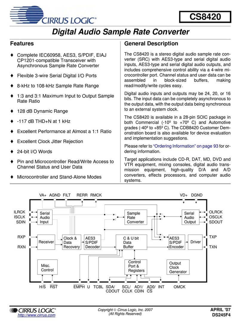
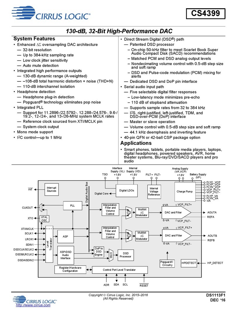
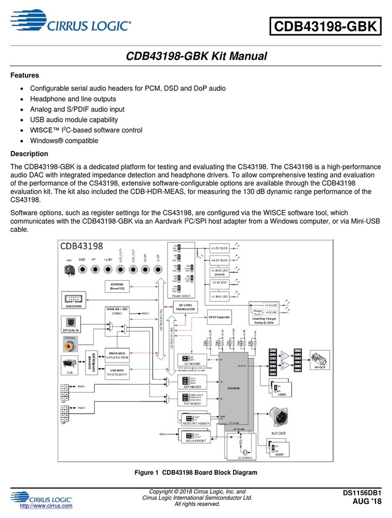
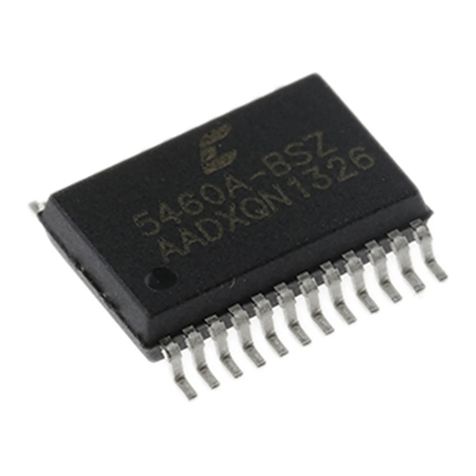
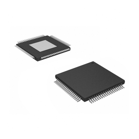
Cirrus Logic CS5530 User manual

Copyright Cirrus Logic, Inc. 2009
(All Rights Reserved)
http://www.cirrus.com
CS5530
24-bit ADC with Ultra-low-noise Amplifier
Features & Description
Chopper-stabilized Instrumentation
Amplifier, 64X
• 12 nV/√Hz @ 0.1 Hz (No 1/f noise)
• 1200 pA Input Current
Digital Gain Scaling up to 40x
Delta-sigma Analog-to-digital Converter
• Linearity Error: 0.0015% FS
• Noise Free Resolution: Up to 19 bits
Scalable VREF Input: Up to Analog Supply
Simple Three-wire Serial Interface
• SPI™ and Microwire™ Compatible
• Schmitt-trigger on Serial Clock (SCLK)
Onboard Offset and Gain Calibration
Registers
Selectable Word Rates: 6.25 to 3,840 Sps
Selectable 50 or 60 Hz Rejection
Power Supply Configurations
• VA+ = +5 V; VA- = 0 V; VD+ = +3 V to +5 V
• VA+ = +2.5 V; VA- = -2.5 V; VD+ = +3 V to +5 V
• VA+ = +3 V; VA- = -3 V; VD+ = +3 V
General Description
The CS5530 is a highly integrated ΔΣ Analog-to-Digital
Converter (ADC) which uses charge-balance techniques
to achieve 24-bit performance. The ADC is optimized for
measuring low-level unipolar or bipolar signals in weigh
scale, process control, scientific, and medical
applications.
To accommodate these applications, the ADC
includes
a very-low-noise, chopper-stabilized instrumentation
amplifier (12 nV/√Hz @ 0.1 Hz) with a gain of 64X. This
device also includes a fourth-order ΔΣ modulator fol-
lowed by a digital filter
which provides twenty selectable
output word rates of 6.25, 7.5, 12.5, 15, 25, 30, 50, 60, 100,
120, 200, 240, 400, 480, 800, 960, 1600, 1920, 3200, and
3840 Sps (MCLK = 4.9152 MHz).
To ease communication between the ADC and a micro-
controller, the converter includes a simple three-wire se-
rial interface which is SPI and Microwire compatible with
a Schmitt-trigger input on the serial clock (SCLK).
High dynamic range, programmable output rates, and
flexible power supply options make this device an ideal
solution for weigh scale and process control
applications.
ORDERING INFORMATION
See page 35.
VA+ C1 C2 VREF+ VREF- VD+
DIFFERENTIAL
4
TH
ORDER
ΔΣ
MODULATOR
PROGRAMMABLE
SINC FIR FILTER
AIN1+
AIN1- SERIAL
INTERFACE
LATCH CLOCK
GENERATOR CALIBRATION
SRAM/CONTROL
LOGIC
DGND
CS
SDI
SDO
SCLK
OSC2OSC1A1A0VA-
64X
NOV ‘09
DS742F3

CS5530
2DS742F3
TABLE OF CONTENTS
1. CHARACTERISTICS AND SPECIFICATIONS .................................................................4
ANALOG CHARACTERISTICS................................................................................4
TYPICAL NOISE-FREE RESOLUTION (BITS)........................................................6
5 V DIGITAL CHARACTERISTICS ..........................................................................7
3 V DIGITAL CHARACTERISTICS ..........................................................................7
DYNAMIC CHARACTERISTICS..............................................................................8
ABSOLUTE MAXIMUM RATINGS...........................................................................8
SWITCHING CHARACTERISTICS..........................................................................9
2. GENERAL DESCRIPTION .............................................................................................. 11
2.1. Analog Input ........................................................................................................... 11
2.1.1. Analog Input Span .......................................................................................... 12
2.1.2. Voltage Noise Density Performance ...........................................................12
2.1.3. No Offset DAC ............................................................................................12
2.2. Overview of ADC Register Structure and Operating Modes .................................. 12
2.2.1. System Initialization ....................................................................................12
2.2.2. Command Register Descriptions ................................................................14
2.2.3. Serial Port Interface .................................................................................... 16
2.2.4. Reading/Writing On-Chip Registers ............................................................ 17
2.3. Configuration Register ...........................................................................................17
2.3.1. Power Consumption ...................................................................................17
2.3.2. System Reset Sequence ............................................................................17
2.3.3. Input Short ..................................................................................................17
2.3.4. Voltage Reference Select ..........................................................................17
2.3.5. Output Latch Pins .......................................................................................18
2.3.6. Filter Rate Select ........................................................................................18
2.3.7. Word Rate Select ........................................................................................18
2.3.8. Unipolar/Bipolar Select ...............................................................................18
2.3.9. Open Circuit Detect ....................................................................................18
2.3.10. Configuration Register Description ...........................................................19
2.4. Calibration ..............................................................................................................21
2.4.1. Calibration Registers ..................................................................................21
2.4.2. Gain Register .............................................................................................21
2.4.3. Offset Register ...........................................................................................21
2.4.4. Performing Calibrations .............................................................................. 22
2.4.5. System Calibration ......................................................................................22
2.4.6. Calibration Tips ...........................................................................................22
2.4.7. Limitations in Calibration Range ................................................................. 23
2.5. Performing Conversions ........................................................................................23
2.5.1. Single Conversion Mode .............................................................................23
2.5.2. Continuous Conversion Mode ....................................................................24
2.6. Using Multiple ADCs Synchronously .....................................................................25
2.7. Conversion Output Coding ....................................................................................25
2.7.1. Conversion Data Output Descriptions ........................................................26
2.8. Digital Filter ............................................................................................................27
2.9. Clock Generator .....................................................................................................28
2.10. Power Supply Arrangements ................................................................................. 28
2.11. Getting Started .......................................................................................................31
2.12. PCB Layout ............................................................................................................ 31
3. PIN DESCRIPTIONS ...................................................................................................... 32
Clock Generator ......................................................................................................32
Control Pins and Serial Data I/O .............................................................................32
Measurement and Reference Inputs ......................................................................33
Power Supply Connections .....................................................................................33
4. SPECIFICATION DEFINITIONS ..................................................................................... 33
5. PACKAGE DRAWINGS .................................................................................................. 34
6. ORDERING INFORMATION .......................................................................................... 35
7. ENVIRONMENTAL, MANUFACTURING, & HANDLING INFORMATION .................... 35

CS5530
DS742F3 3
LIST OF FIGURES
Figure 1. SDI Write Timing (Not to Scale)...............................................................................10
Figure 2. SDO Read Timing (Not to Scale).............................................................................10
Figure 3. Front End Configuration...........................................................................................11
Figure 4. Input Model for AIN+ and AIN- Pins.........................................................................11
Figure 5. Measured Voltage Noise Density.............................................................................12
Figure 5. Measured Voltage Noise Density.............................................................................12
Figure 6. CS5530 Register Diagram.......................................................................................13
Figure 7. Command and Data Word Timing ...........................................................................16
Figure 8. Input Reference Model when VRS = 1 ....................................................................18
Figure 9. Input Reference Model when VRS = 0 ....................................................................18
Figure 10. System Calibration of Offset..................................................................................22
Figure 11. System Calibration of Gain....................................................................................22
Figure 12. Synchronizing Multiple ADCs.................................................................................25
Figure 13. Digital Filter Response (Word Rate = 60 Sps).......................................................27
Figure 14. 120 Sps Filter Magnitude Plot to 120 Hz ...............................................................27
Figure 15. 120 Sps Filter Phase Plot to 120 Hz......................................................................27
Figure 16. Z-Transforms of Digital Filters................................................................................27
Figure 17. On-chip Oscillator Model........................................................................................28
Figure 18. CS5530 Configured with a Single +5 V Supply .....................................................29
Figure 19. CS5530 Configured with ±2.5 V Analog Supplies..................................................29
Figure 20. CS5530 Configured with ±3 V Analog Supplies.....................................................30
LIST OF TABLES
Table 1. Conversion Timing for Single Mode..........................................................................24
Table 2. Conversion Timing for Continuous Mode..................................................................24
Table 3. Output Coding...........................................................................................................25

CS5530
4DS742F3
1. CHARACTERISTICS AND SPECIFICATIONS
ANALOG CHARCTERISTICS
(VA+, VD+ = 5 V ±5%; VREF+ = 5 V; VA-, VREF-, DGND = 0 V; MCLK = 4.9152 MHz;
OWR (Output Word Rate) = 60 Sps; Bipolar Mode)
(See Notes 1 and 2.)
Notes: 1. Applies after system calibration at any temperature within -40 °C to +85 °C.
2. Specifications guaranteed by design, characterization, and/or test. LSB is 24 bits.
3. This specification applies to the device only and does not include any effects by external parasitic
thermocouples.
4. Drift over specified temperature range after calibration at power-up at 25 °C.
Parameter CS5530-CS UnitMin Typ Max
Accuracy
Linearity Error - ±0.0015 ±0.003 %FS
No Missing Codes 24 - - Bits
Bipolar Offset - ±16 ±32 LSB24
Unipolar Offset - ±32 ±64 LSB24
Offset Drift (Notes 3 and 4) - 10 - nV/°C
Bipolar full-scale Error - ±8±31 ppm
Unipolar full-scale Error - ±16 ±62 ppm
full-scale Drift (Note 4) - 2 - ppm/°C

CS5530
DS742F3 5
ANALOG CHARACTERISTICS (Continued)
(See Notes 1 and 2.)
Notes: 5. See the section of the data sheet which discusses input models.
6. Input current on VREF+ or VREF- may increase to 250 nA if operated within 50 mV of VA+ or VA-.This
is due to the rough charge buffer being saturated under these conditions.
Parameter Min Typ Max Unit
Analog Input
Common Mode + Signal on AIN+ or AIN- Bipolar/Unipolar Mode (VA-) + 1.6 - (VA+) - 1.6 V
CVF Current on AIN+ or AIN- - 1200 - pA
Input Current Noise - 1 - pA/√Hz
Open Circuit Detect Current 100 300 - nA
Common Mode Rejection DC
50, 60 Hz -
-130
120 -
-dB
dB
Input Capacitance - 10 - pF
Voltage Reference Input
Range (VREF+) - (VREF-) 1 2.5 (VA+)-(VA-) V
CVF Current (Note 5, 6) - 50 - nA
Common Mode Rejection DC
50, 60 Hz -
-120
120 -
-dB
dB
Input Capacitance 11 - 22 pF
System Calibration Specifications
Full-scale Calibration Range Bipolar/Unipolar Mode 3 - 110 %FS
Offset Calibration Range Bipolar Mode -100 - 100 %FS
Offset Calibration Range Unipolar Mode -90 - 90 %FS

CS5530
6DS742F3
ANALOG CHARACTERISTICS (Continued)
(See Notes 1 and 2.)
7. All outputs unloaded. All input CMOS levels.
8. Tested with 100 mV change on VA+ or VA-.
TYPICAL NOISE-FREE RESOLUTION (BITS) (See Notes 9 and 10)
9. Noise Free Resolution listed is for Bipolar operation, and is calculated as LOG((Input Span)/(6.6xRMS
Noise))/LOG(2) rounded to the nearest bit. For Unipolar operation, the input span is 1/2 as large, so one
bit is lost. The input span is calculated in the analog input span section of the data sheet. The Noise
Free Resolution table is computed with a value of 1.0 in the gain register. Values other than 1.0 will
scale the noise, and change the Noise Free Resolution accordingly.
10. “Noise Free Resolution” is not the same as “Effective Resolution”. Effective Resolution is based on the
RMS noise value, while Noise Free Resolution is based on a peak-to-peak noise value specified as 6.6
times the RMS noise value. Effective Resolution is calculated as LOG((Input Span)/(RMS
Noise))/LOG(2).
Specifications are subject to change without notice.
Parameter
CS5530-CS
Min Typ Max Unit
Power Supplies
DC Power Supply Currents (Normal Mode) IA+, IA-
ID+
-
-
6
0.6 8
1.0 mA
mA
Power Consumption Normal Mode (Note 7)
Standby
Sleep
-
-
-
35
5
500
45
-
-
mW
mW
µW
Power Supply Rejection (Note 8)
DC Positive Supplies
DC Negative Supply -
-115
115 -
-dB
dB
Output Word Rate (Sps) -3 dB Filter Frequency (Hz) Noise-free Bits Noise (nVrms)
7.5 1.94 19 17
15 3.88 19 24
30 7.75 18 34
60 15.5 18 48
120 31 17 68
240 62 16 115
480 122 16 163
960 230 15 229
1,920 390 15 344
3,840 780 13 1390

CS5530
DS742F3 7
5 V DIGITAL CHARACTERISTICS
(VA+, VD+ = 5 V ±5%; VA-, DGND = 0 V; See Notes 2 and 11.)
3 V DIGITAL CHARACTERISTICS
(TA= 25 °C; VA+ = 5V ±5%; VD+ = 3.0V±10%; VA-, DGND = 0V; See Notes 2 and 11.)
11. All measurements performed under static conditions.
Parameter Symbol Min Typ Max Unit
High-Level Input Voltage All Pins Except SCLK
SCLK VIH 0.6 VD+
(VD+) - 0.45 -
-VD+
VD+ V
Low-Level Input Voltage All Pins Except SCLK
SCLK VIL 0.0
0.0 -0.8
0.6 V
High-Level Output Voltage A0 and A1, Iout = -1.0 mA
SDO, Iout = -5.0 mA VOH (VA+) - 1.0
(VD+) - 1.0 --V
Low-Level Output Voltage A0 and A1, Iout = 1.0 mA
SDO, Iout = 5.0 mA VOL - - (VA-) + 0.4
0.4 V
Input Leakage Current Iin -±1±10µA
SDO 3-State Leakage Current IOZ --±10µA
Digital Output Pin Capacitance Cout -9-pF
Parameter Symbol Min Typ Max Unit
High-Level Input Voltage All Pins Except SCLK
SCLK VIH 0.6 VD+
(VD+) - 0.45 -VD+
VD+ V
Low-Level Input Voltage All Pins Except SCLK
SCLK VIL 0.0
0.0 -0.8
0.6 V
High-Level Output Voltage A0 and A1, Iout = -1.0 mA
SDO, Iout = -5.0 mA VOH (VA+) - 1.0
(VD+) - 1.0 --V
Low-Level Output Voltage A0 and A1, Iout = 1.0 mA
SDO, Iout = 5.0 mA VOL - - (VA-) + 0.4
0.4 V
Input Leakage Current Iin -±1±10µA
SDO 3-State Leakage Current IOZ --±10µA
Digital Output Pin Capacitance Cout -9-pF

CS5530
8DS742F3
DYNAMIC CHARACTERISTICS
12. The ADCs use a Sinc5filter for the 3200 Sps and 3840 Sps output word rate (OWR) and a Sinc5filter
followed by a Sinc3filter for the other OWRs. OWRsinc5 refers to the 3200 Sps (FRS = 1) or 3840 Sps
(FRS = 0) word rate associated with the Sinc5filter.
13. The single conversion mode only outputs fully settled conversions. See Table 1 for more details about
single conversion mode timing. OWRSC is used here to designate the different conversion time
associated with single conversions.
14. The continuous conversion mode outputs every conversion. This means that the filter’s settling time
with a full-scale step input in the continuous conversion mode is dictated by the OWR.
ABSOLUTE MAXIMUM RATINGS
(DGND = 0 V; See Note 15.)
Notes: 15. All voltages with respect to ground.
16. VA+ and VA- must satisfy {(VA+) - (VA-)} ≤+6.6 V.
17. VD+ and VA- must satisfy {(VD+) - (VA-)} ≤ +7.5 V.
18. Applies to all pins including continuous overvoltage conditions at the analog input (AIN) pins.
19. Transient current of up to 100 mA will not cause SCR latch-up. Maximum input current for a power
supply pin is ±50 mA.
20. Total power dissipation, including all input currents and output currents.
WARNING: Operation at or beyond these limits may result in permanent damage to the device.
Normal operation is not guaranteed at these extremes.
Parameter Symbol Ratio Unit
Modulator Sampling Rate fsMCLK/16 Sps
Filter Settling Time to 1/2 LSB (full-scale Step Input)
Single Conversion mode (Notes 12, 13, and 14)
Continuous Conversion mode, OWR < 3200 Sps
Continuous Conversion mode, OWR ≥3200 Sps
ts
ts
ts
1/OWRSC
5/OWRsinc5 + 3/OWR
5/OWR
s
s
s
Parameter Symbol Min Typ Max Unit
DC Power Supplies (Notes 16 and 17)
Positive Digital
Positive Analog
Negative Analog
VD+
VA+
VA-
-0.3
-0.3
+0.3
-
-
-
+6.0
+6.0
-3.75
V
V
V
Input Current, Any Pin Except Supplies (Notes 18 and 19) IIN --±10mA
Output Current IOUT --±25mA
Power Dissipation (Note 20) PDN - - 500 mW
Analog Input Voltage VREF pins
AIN Pins VINR
VINA
(VA-) -0.3
(VA-) -0.3 -
-(VA+) + 0.3
(VA+) + 0.3 V
V
Digital Input Voltage VIND -0.3 - (VD+) + 0.3 V
Ambient Operating Temperature TA-40 - 85 °C
Storage Temperature Tstg -65 - 150 °C

CS5530
DS742F3 9
SWITCHING CHARACTERISTICS
(VA+ = 2.5 V or 5 V ±5%; VA- = -2.5V±5% or 0 V; VD+ = 3.0 V ±10% or 5 V ±5%;DGND = 0 V; Levels: Logic 0 = 0
V, Logic 1 = VD+; CL= 50 pF; See Figures 1 and 2.)
Notes: 21. Device parameters are specified with a 4.9152 MHz clock.
22. Specified using 10% and 90% points on waveform of interest. Output loaded with 50 pF.
23. Oscillator start-up time varies with crystal parameters. This specification does not apply when using an
external clock source.
Parameter Symbol Min Typ Max Unit
Master Clock Frequency (Note 21)
External Clock or Crystal Oscillator MCLK 1 4.9152 5 MHz
Master Clock Duty Cycle 40 - 60 %
Rise Times (Note 22)
Any Digital Input Except SCLK
SCLK
Any Digital Output
trise -
-
-
-
-
50
1.0
100
-
µs
µs
ns
Fall Times (Note 22)
Any Digital Input Except SCLK
SCLK
Any Digital Output
tfall -
-
-
-
-
50
1.0
100
-
µs
µs
ns
Start-up
Oscillator Start-up Time XTAL = 4.9152 MHz (Note 23) tost -20-ms
Serial Port Timing
Serial Clock Frequency SCLK 0 - 2 MHz
Serial Clock Pulse Width High
Pulse Width Low t1
t2
250
250 -
--
-ns
ns
SDI Write Timing
CS Enable to Valid Latch Clock t350 - - ns
Data Set-up Time prior to SCLK rising t450 - - ns
Data Hold Time After SCLK Rising t5100 - - ns
SCLK Falling Prior to CS Disable t6100 - - ns
SDO Read Timing
CS to Data Valid t7--150ns
SCLK Falling to New Data Bit t8--150ns
CS Rising to SDO Hi-Z t9--150ns

CS5530
DS742F3 11
2. GENERAL DESCRIPTION
The CS5530 is a ΔΣ Analog-to-Digital Converter
(ADC) which uses charge-balance techniques to
achieve 24-bit performance. The ADC is optimized
for measuring low-level unipolar or bipolar signals
in weigh scale, process control, scientific, and med-
ical applications.
To accommodate these applications, the ADC
in-
cludes a very-low-noise, chopper-stabilized instru-
mentation amplifier (12 nV/√Hz @ 0.1 Hz) with a
gain of 64X. This ADC also includes a fourth-order
ΔΣ modulator followed by a digital filter
which pro-
vides twenty selectable output word rates of 6.25,
7.5, 12.5, 15, 25, 30, 50, 60, 100, 120, 200, 240, 400,
480, 800, 960, 1600, 1920, 3200, and 3840 samples
per second (MCLK = 4.9152 MHz).
To ease communication between the ADCs and a
micro-controller, the converters include a simple
three-wire serial interface which is SPI and Mi-
crowire compatible with a Schmitt-trigger input on
the serial clock (SCLK).
2.1 Analog Input
Figure 3 illustrates a block diagram of the CS5530.
The front end includes a chopper-stabilized instru-
mentation amplifier with a gain of 64X.
The amplifier is chopper-stabilized and operates with
a chop clock frequency of MCLK/128. The CVF
(sampling) current into the instrumentation amplifier
is typically 1200 pA over -40°C to +85°C
(MCLK=4.9152 MHz). The common-mode plus sig-
nal range of the instrumentation amplifier is (VA-) +
1.6 V to (VA+) - 1.6 V.
Figure 4illustrates the input model for the 64X am-
plifier.
Note: The C = 3.9 pF capacitor is for input current
modelingonly.Forphysicalinputcapacitance
see ‘Input Capacitance’ specification under
Analog Characteristics.
VREF+
Sinc
Digital
Filter
64x
AIN+
AIN-
X1
VREF-
X1
Differential
4 Order
ΔΣ
Modulator
th 5Programmable
Sinc
Digital Filter
3Serial
Port
1000Ω
1000Ω
22 nF C1 PIN
C2 PIN
Figure 3. Front End Configuration
AIN C=3.9pF
f =
V ≤8 mV
i = fV C
os os
nMCLK
128
Figure 4. Input Model for AIN+ and AIN- Pins

CS5530
12 DS742F3
2.1.1 Analog Input Span
The full-scale input signal that the converter can dig-
itize is a function of the reference voltage connected
between the VREF+ and VREF- pins. The full-scale
input span of the converter is
((VREF+) –(VREF-))/(64Y), where 64 is the gain
of the amplifier and Y is 2 for VRS = 0, or Y is 1 for
VRS = 1. VRS is the Voltage Reference Select bit,
and must be set according to the differential voltage
applied to the VREF+ and VREF- pins on the part.
See section 2.3.4 for more details.
With a 2.5 V reference, the full-scale biploar input
range is equal to ±2.5/64, or about ±39 mV. Note
that these input ranges assume the calibration regis-
ters are set to their default values (i.e. Gain = 1.0 and
Offset = 0.0). The gain setting in the Gain Register
can be altered to map the digital codes of the con-
verter to set full scales from 1 mV to 40 mV.
2.1.2 Voltage Noise Density Performance
Figure 5 illustrates the measured voltage noise den-
sity versus frequency from 0.025 Hz to 10 Hz. The
device was powered with ±2.5 V supplies, using
30 Sps OWR, bipolar mode, and with the input
short bit enabled.
2.1.3 No Offset DAC
An offset DAC was not included in the CS5530 be-
cause the high dynamic range of the converter
eliminates the need for one. The offset register can
be manipulated by the user to mimic the function of
a DAC if desired.
2.2 Overview of ADC Register Structure
and Operating Modes
The CS5530 ADC has an on-chip controller, which
includes a number of user-accessible registers. The
registers are used to hold offset and gain calibration
results, configure the chip's operating modes, hold
conversion instructions, and to store conversion
data words. Figure 6 depicts a block diagram of the
on-chip controller’s internal registers.
The converter has 32-bit registers to function as the
offset and the gain calibration registers. These reg-
isters hold calibration results. The contents of these
registers can be read or written by the user. This al-
lows calibration data to be off-loaded into an exter-
nal EEPROM. The user can also manipulate the
contents of these registers to modify the offset or
the gain slope of the converter.
The converter includes a 32-bit configuration reg-
ister which is used for setting options such as the
power down modes, resetting the converter, short-
ing the analog input, enabling logic outputs, and
other user options.
The following pages document how to initialize the
converter and perform offset and gain calibrations.
Each of the bits of the configuration register is de-
scribed. Also the Command Register Quick Refer-
ence can be used to decode all valid commands (the
first 8-bits into the serial port).
2.2.1 System Initialization
The CS5530 provide no power-on-reset function.
To initialize the ADC, the user must perform a soft-
ware reset via the configuration register. Before
accessing the configuration register, the user must
insure serial port synchronization by using the Se-
rial Port Initialization sequence. This sequence re-
sets the serial port to the command mode and is
accomplished by transmitting at least 15 SYNC1
command bytes (0xFF hexadecimal), followed by
one SYNC0 command (0xFE hexadecimal). Note
that this sequence can be initiated at anytime to
reinitialize the serial port. To complete the system
1
10
100
1000
0.025 0.10 1.00 10.00
Frequency (Hz)
Figure 5. Measured Voltage Noise Density, 64x

CS5530
DS742F3 13
initialization sequence, the user must also perform
a system reset sequence which is as follows: Write
a logic 1 into the RS bit of the configuration regis-
ter. This will reset the calibration registers and
other logic (but not the serial port). A valid reset
will set the RV bit in the configuration register to a
logic 1. After writing the RS bit to a logic 1, wait
8 master clock cycles, then write the RS bit back to
logic 0. Note that the other bits in the configura-
tion register cannot be written on this write cycle
as they are being held in reset until RS is set back
to logic 0. While this involves writing an entire
word into the configuration register to casue the
RS bit to go to logic 0, the RV bit is a read only bit,
therefore a write to the configuration register will
not overwrite the RV bit. After clearing the RS bit
back to logic 0, read the configuration register to
check the state of the RV bit as this indicates that a
valid reset occurred. Reading the configuration
register clears the RV bit back to logic 0.
Completing the reset cycle initializes the on-chip
registers to the following states:
After the configuration register has been read to
clear the RV bit, the register can then be written to
set the other function bits or other registers can be
written or read.
Once the system initialization or reset is complet-
ed, the on-chip controller is initialized into com-
mand mode where it waits for a valid command
(the first 8-bits written into the serial port are shift-
ed into the command register). Once a valid com-
mand is received and decoded, the byte instructs
the converter to either acquire data from or transfer
data to an internal register, or perform a conversion
or a calibration. The Command Register Descrip-
tions section lists all valid commands.
Offset (1 x 32)
Offset Register (1 x 32)
Conversion Data
Register (1 x 32)
Configuration Register (1 x 32)
Power Save Select
Reset System
Input Short
Voltage Reference Select
Output Latch
CS
SDI
SDO
SCLK
Read Only
Command
Register (1 × 8)
Write Only
Serial
Interface
Data (1 x 32)
Filter Rate Select
Word Rate
Unipolar/Bipolar
Open Circuit Detect
Gain (1 x 32)
Gain Register (1 x 32)
Figure 6. CS5530 Register Diagram
Configuration Register: 00000000(H)
Offset Register: 00000000(H)
Gain Register 01000000(H)

CS5530
14 DS742F3
2.2.2 Command Register Descriptions
READ/WRITE OFFSET REGISTER
R/W (Read/Write)
0 Write offset register.
1 Read offset register.
READ/WRITE GAIN REGISTER
R/W (Read/Write)
0 Write gain register.
1 Read gain register.
READ/WRITE CONFIGURATION REGISTER
Function: These commands are used to read from or write to the configuration register.
R/W (Read/Write)
0 Write configuration register.
1 Read configuration register.
PERFORM CONVERSION
MC (Multiple Conversions)
0 Perform a single conversion.
1 Perform continuous conversions.
PERFORM SYSTEM OFFSET CALIBRATION
PERFORM SYSTEM GAIN CALIBRATION
SYNC1
Function: Part of the serial port re-initialization sequence.
D7(MSB) D6 D5 D4 D3 D2 D1 D0
0000R/W001
D7(MSB) D6 D5 D4 D3 D2 D1 D0
0000R/W010
D7(MSB) D6 D5 D4 D3 D2 D1 D0
0000R/W
011
D7(MSB) D6 D5 D4 D3 D2 D1 D0
1MC000000
D7(MSB) D6 D5 D4 D3 D2 D1 D0
10000101
D7(MSB) D6 D5 D4 D3 D2 D1 D0
10000110
D7(MSB) D6 D5 D4 D3 D2 D1 D0
11111111

CS5530
16 DS742F3
2.2.3 Serial Port Interface
The CS5530’s serial interface consists of four con-
trol lines: CS, SDI, SDO, SCLK. Figure 7 details
the command and data word timing.
CS, Chip Select, is the control line which enables
access to the serial port. If the CS pin is tied low,
the port can function as a three wire interface.
SDI, Serial Data In, is the data signal used to trans-
fer data to the converters.
SDO, Serial Data Out, is the data signal used to
transfer output data from the converters. The SDO
output will be held at high impedance any time CS
is at logic 1.
SCLK, Serial Clock, is the serial bit-clock which
controls the shifting of data to or from the ADC’s
serial port. The CS pin must be held low (logic 0)
before SCLK transitions can be recognized by the
port logic. To accommodate optoisolators SCLK is
designed with a Schmitt-trigger input to allow an
optoisolator with slower rise and fall times to di-
rectly drive the pin. Additionally, SDO is capable
of sinking or sourcing up to 5 mA to directly drive
an optoisolator LED. SDO will have less than a 400
mV loss in the drive voltage when sinking or sourc-
ing 5 mA.
Command Time
8SCLKs Data Time 32 SCLKs
Write Cycle
CS
SCLK
SDI
MSB
Command Time
8SCLKs
CS
SCLK
SDI
Read Cycle
SDO
MSB LSB
Command Time
8SCLKs
8 SCLKs Clear SDO Flag
SDO
SCLK
SDI
MSB LSB
Clock Cycles
t*
d
CS
Data Time 32 SCLKs
Data Time 32 SCLKs
LSB
Data Conversion Cycle
/OWR
MCLK
* td is the time it takes the ADC to perform a conversion. See the Single
Conversion and Continuous Conversion sections of the data sheet for more
details about conversion timing.
Figure 7. Command and Data Word Timing

CS5530
DS742F3 17
2.2.4 Reading/Writing On-Chip Registers
The CS5530’s offset, gain, and configuration regis-
ters are readable and writable while the conversion
data register is read only.
As shown in Figure 7, to write to a particular regis-
ter the user must transmit the appropriate write
command and then follow that command by 32 bits
of data. For example, to write 0x80000000 (hexa-
decimal) to the gain register, the user would first
transmit the command byte 0x02 (hexadecimal)
followed by the data 0x80000000 (hexadecimal).
Similarly, to read a particular register the user must
transmit the appropriate read command and then
acquire the 32 bits of data. Once a register is written
to or read from, the serial port returns to the com-
mand mode.
2.3 Configuration Register
To ease the architectural design and simplify the
serial interface, the configuration register is thirty-
two bits long, however, only fifteen of the thirty
two bits are used. The following sections detail the
bits in the configuration register.
2.3.1 Power Consumption
The CS5530 accommodates three power consump-
tion modes: normal, standby, and sleep. The default
mode, “normal mode”, is entered after power is ap-
plied. In this mode, the CS5530 typically consumes
35 mW. The other two modes are referred to as the
power save modes. They power down most of the
analog portion of the chip and stop filter convolu-
tions. The power save modes are entered whenever
the power down (PDW) bit of the configuration
register is set to logic 1. The particular power save
mode entered depends on state of the PSS (Power
Save Select) bit. If PSS is logic 0, the converter en-
ters the standby mode reducing the power con-
sumption to 4 mW. The standby mode leaves the
oscillator and the on-chip bias generator for the an-
alog portion of the chip active. This allows the con-
verter to quickly return to the normal mode once
PDW is set back to a logic 0. If PSS and PDW are
both set to logic 1, the sleep mode is entered reduc-
ing the consumed power to around 500 μW. Since
this sleep mode disables the oscillator, approxi-
mately a 20 ms oscillator start-up delay period is
required before returning to the normal mode. If an
external clock is used, there will be no delay.
2.3.2 System Reset Sequence
The reset system (RS) bit permits the user to per-
form a system reset. A system reset can be initiated
at any time by writing a logic 1 to the RS bit in the
configuration register. After the RS bit has been
set, the internal logic of the chip will be initialized
to a reset state. The reset valid (RV) bit is set indi-
cating that the internal logic was properly reset.
The RV bit is cleared after the configuration regis-
ter is read. The on-chip registers are initialized to
the following default states:
After reset, the RS bit should be written back to
logic 0 to complete the reset cycle. The ADC will
return to the command mode where it waits for a
valid command. Also, the RS bit is the only bit in
the configuration register that can be set when ini-
tiating a reset (i.e. a second write command is need-
ed to set other bits in the Configuration Register
after the RS bit has been cleared).
2.3.3 Input Short
The input short bit allows the user to internally
ground the inputs of the ADC. This is a useful func-
tion because it allows the user to easily test the
grounded input performance of the ADC and elim-
inate the noise effects due to the external system
components.
2.3.4 Voltage Reference Select
The voltage reference select (VRS) bit selects the
size of the sampling capacitor used to sample the
voltage reference. The bit should be set based upon
Configuration Register: 00000000(H)
Offset Register: 00000000(H)
Gain Register 01000000(H)

CS5530
18 DS742F3
the magnitude of the reference voltage to achieve
optimal performance. Figures 8 and 9 model the ef-
fects on the reference’s input impedance and input
current for each VRS setting. As the models show,
the reference includes a coarse/fine charge buffer
which reduces the dynamic current demand of the
external reference.
The reference’s input buffer is designed to accom-
modate rail-to-rail (common-mode plus signal) in-
put voltages. The differential voltage between the
VREF+ and VREF- can be any voltage from 1.0 V
up to the analog supply (depending on how VRS is
configured), however, the VREF+ cannot go above
VA+ and the VREF- pin can not go below VA-.
Note that the power supplies to the chip should be
established before the reference voltage.
2.3.5 Output Latch Pins
The A1-A0 pins of the ADC mimic the D24-D23
bits of the configuration register. A1-A0 can be
used to control external multiplexers and other log-
ic functions outside the converter. The A1-A0 out-
puts can sink or source at least 1 mA, but it is
recommended to limit drive currents to less than
20 μA to reduce self-heating of the chip. These out-
puts are powered from VA+ and VA-. Their output
voltage will be limited to the VA+ voltage for a
logic 1 and VA- for a logic 0. Note that if the latch
bits are used to modify the analog input signal the
user should delay performing a conversion until he
knows the effects of the A0/A1 bits are fully set-
tled.
2.3.6 Filter Rate Select
The Filter Rate Select bit (FRS) modifies the output
word rates of the converter to allow either 50 Hz or
60 Hz rejection when operating from a 4.9152
MHz crystal. If FRS is cleared to logic 0, the word
rates and corresponding filter characteristics can be
selected using the Configuration Register. Rates
can be 7.5, 15, 30, 60, 120, 240, 480, 960, 1920, or
3840 Sps when using a 4.9152 MHz clock. If FRS
is set to logic 1, the word rates and corresponding
filter characteristics scale by a factor of 5/6, mak-
ing the selectable word rates 6.25, 12.5, 25, 50,
100, 200, 400, 800, 1600, and 3200 Sps when using
a 4.9152 MHz clock. When using other clock fre-
quencies, these selectable word rates will scale lin-
early with the clock frequency that is used.
2.3.7 Word Rate Select
The Word Rate Select bits (WR3-WR0) allow slec-
tion of the output word rate of the converter as de-
picted in the Configuration Register Descriptions.
The word rate chosen by the WR3-WR0 bits is
modified by the setting of the FRS bit as presented
in the previous paragraph.
2.3.8 Unipolar/Bipolar Select
The UP/BP Select bit sets the converter to measure
either a unipolar or bipolar input span.
2.3.9 Open Circuit Detect
When the OCD bit is set it activates a current
source as a means to test for open thermocouples.
VREF
C=14pF
f=
2
φFine
1
V≤8mV
i=fV C
os
os
n
φCoarse
MCLK
16
VRS = 1; 1 V ≤V≤ 2.5 V
REF
Figure 8. Input Reference Model when VRS = 1
VREF
C= 7pF
f=
2
φFine
1
V≤16 mV
i=fV C
os
osn
φCoarse
MCLK
16
VRS = 0; 2.5 V < V ≤ VA+
REF
Figure 9. Input Reference Model when VRS = 0

CS5530
DS742F3 19
2.3.10 Configuration Register Description
PSS (Power Save Select)[31]
0 Standby Mode (Oscillator active, allows quick power-up).
1 Sleep Mode (Oscillator inactive).
PDW (Power Down Mode)[30]
0 Normal Mode
1 Activate the power save select mode.
RS (Reset System)[29]
0 Normal Operation.
1 Activate a Reset cycle. See System Reset Sequence in the datasheet text.
RV (Reset Valid)[28]
0 Normal Operation
1 System was reset. This bit is read only. Bit is cleared to logic zero after the configuration register is read.
IS (Input Short)[27]
0 Normal Input
1 All signal input pairs for each channel are disconnected from the pins and shorted internally.
NU (Not Used)[26]
0 Must always be logic 0. Reserved for future upgrades.
VRS (Voltage Reference Select)[25]
0 2.5 V < VREF ≤[(VA+) - (VA-)]
11V≤VREF ≤2.5V
A1-A0 (Output Latch bits)[24:23]
The latch bits (A1 and A0) will be set to the logic state of these bits when the Configuration register is written.
Note that these logic outputs are powered from VA+ and VA-.
00 A1 = 0, A0 = 0
01 A1 = 0, A0 = 1
10 A1 = 1, A0 = 0
11 A1 = 1, A0 = 1
NU (Not Used)[22:20]
0 Must always be logic 0. Reserved for future upgrades.
Filter Rate Select, FRS[19]
0 Use the default output word rates.
1 Scale all output word rates and their corresponding filter characteristics by a factor of 5/6.
NU (Not Used)[18:15]
0 Must always be logic 0. Reserved for future upgrades.
D31(MSB) D30 D29 D28 D27 D26 D25 D24 D23 D22 D21 D20 D19 D18 D17 D16
PSS PDW RS RV IS NU VRS A1 A0 NU NU NU FRS NU NU NU
D15 D14D13D12D11D10D9D8D7D6D5D4D3D2D1D0
NU WR3 WR2 WR1 WR0 UP/BP OCDNUNUNUNUNUNUNUNUNU

CS5530
20 DS742F3
WR3-WR0 (Word Rate) [14:11]
The listed Word Rates are for continuous conversion mode using a 4.9152 MHz clock. All word rates will
scale linearly with the clock frequency used. The very first conversion using continuous conversion mode
will last longer, as will conversions done with the single conversion mode. See the section on Performing
Conversions and Tables 1 and 2 for more details.
Bit WR (FRS = 0) WR (FRS = 1)
0000 120 Sps 100 Sps
0001 60 Sps 50 Sps
0010 30 Sps 25 Sps
0011 15 Sps 12.5 Sps
0100 7.5 Sps 6.25 Sps
1000 3840 Sps 3200 Sps
1001 1920 Sps 1600 Sps
1010 960 Sps 800 Sps
1011 480 Sps 400 Sps
1100 240 Sps 200 Sps
All other combinations are not used.
U/B (Unipolar / Bipolar) [10]
0 Select Bipolar mode.
1 Select Unipolar mode.
OCD (Open Circuit Detect Bit) [9]
When set, this bit activates a 300 nA current source on the input channel (AIN+) selected by the channel
select bits. Note that the 300nA current source is rated at 25°C. This feature is particularly useful in ther-
mocouple applications when the user wants to drive a suspected open thermocouple lead to a supply rail.
0 Normal mode.
1 Activate current source.
NU (Not Used) [8:0]
0 Must always be logic 0. Reserved for future upgrades.
Table of contents
Other Cirrus Logic Media Converter manuals
Popular Media Converter manuals by other brands
Fagor
Fagor G2AI installation manual
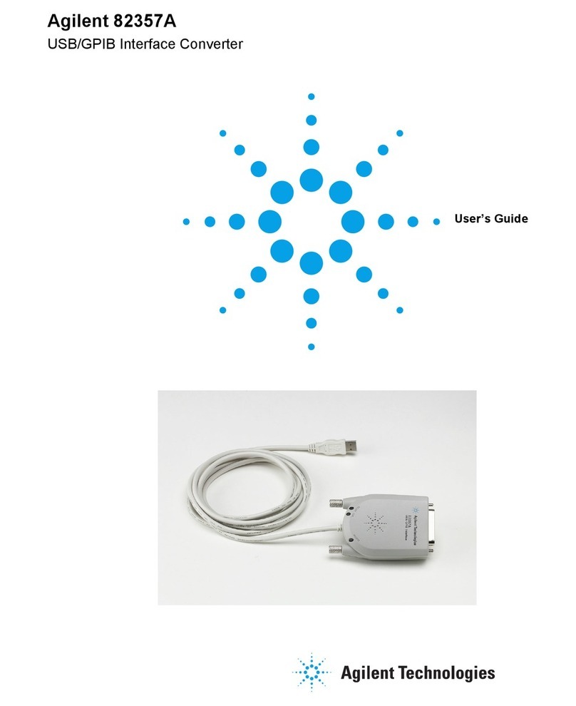
Agilent Technologies
Agilent Technologies USB/GPIB Interface Converter 82357A user guide

HEAD
HEAD BLACK HAWK Z user manual
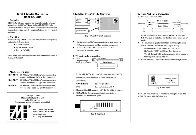
Moxa Technologies
Moxa Technologies ME50-M-SC user guide
Miranda
Miranda DENSITE IRD-3101 Guide to installation and operation

Memphis
Memphis LL2BE quick start guide


