1
Document change history
・
Added the descriptions on CPU core "ARM" and "PALMiCE3 ARM (JTAG200)" to Technical
Information reference chart and Product purchase chart.
・Corrected the Product purchase chart.
Technical Information ④and ⑥correspond to PALMiCE3 CM3 (ETM200) only.
However, PALMiCE3 CM3(ETM200) is a product to be released in the future.
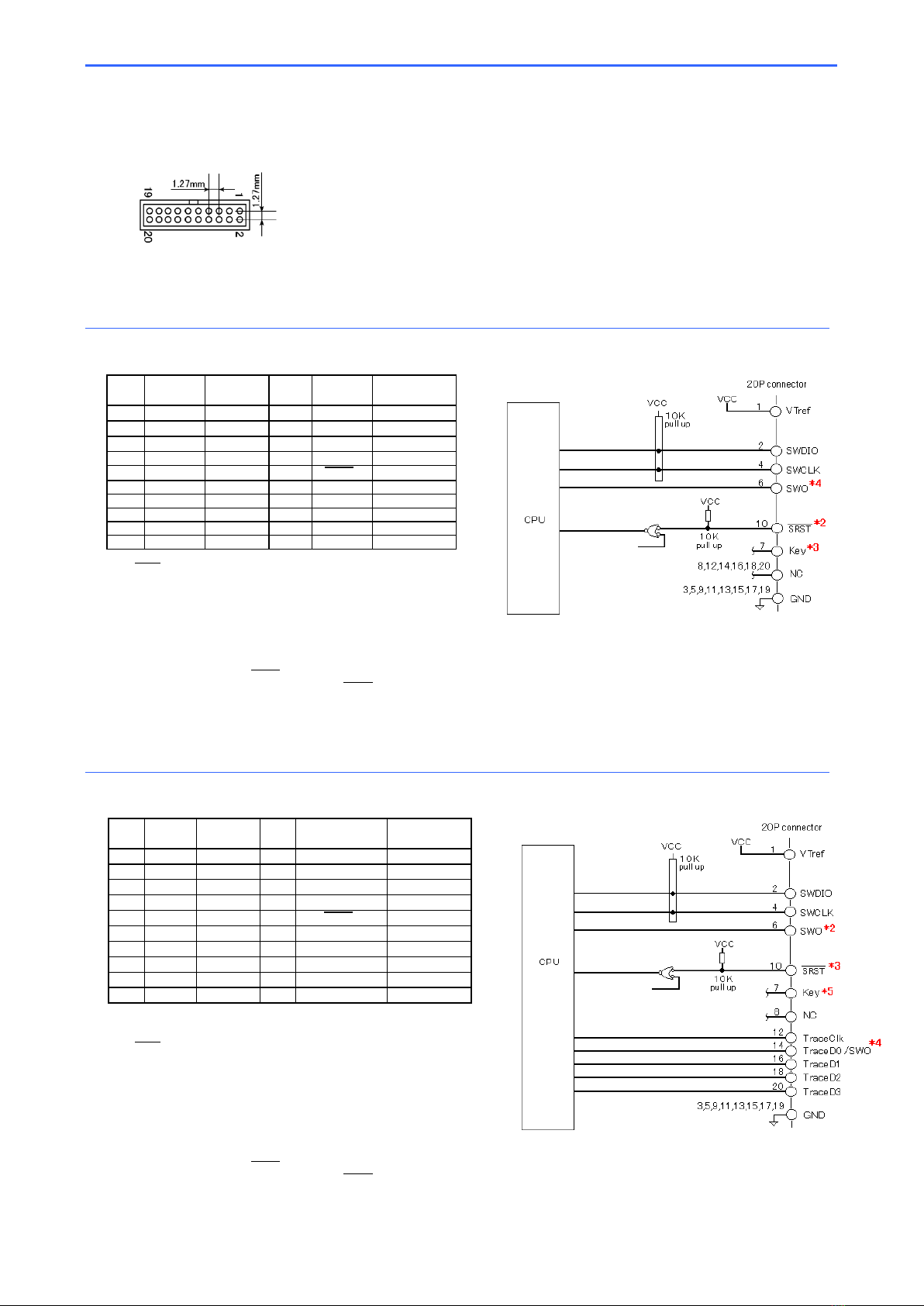
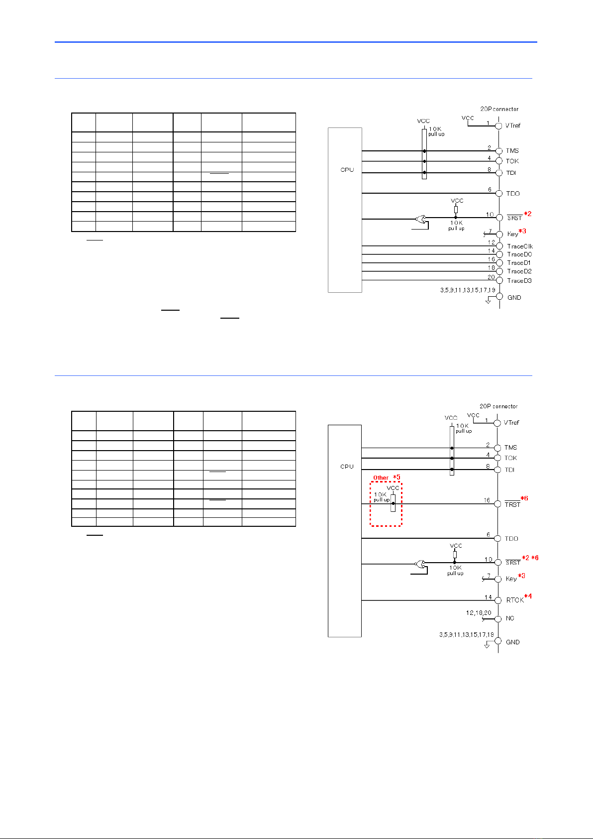
・Added the note on SRST signal in respective signal tables.
”SRST signal is an open-collector output."
・
PALMiCE3 CM3(ETM200) has already been released (Dec. 2009).
Deleted the following description:
”To be released in the future.”
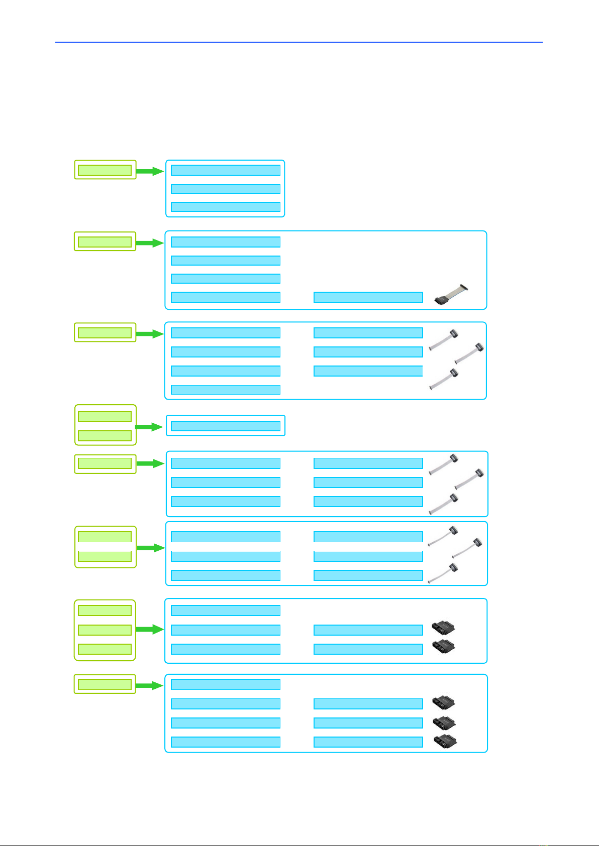
・“Supported connectors”
Added graphic images of the connectors.
・“Product purchase chart”
Added graphic images of the optional products.
・Added the note on SRST signal in respective signal tables.
・Changed the note on TRST signal in respective signal tables.
・Deleted CPU core options from Technical Information reference chart and Product purchase
chart.
For supported CPUs, refer to Product Summary of respective products up on our website.
・Deleted the description of the case where ETM is not used and half-pitch (1.27mm) connector is
used.
When you use them, please contact us.
・
Added an item to Applicable products:
PALMiCE2H ARM (ETM383)
・Following addition of an item to Applicable products mentioned above, added the description on
PALMiCE2H to Technical Information reference chart and Product purchase chart.
・Following addition of an item to Applicable products mentioned above, added ⑦⑧⑨⑩ to pages
on target interface details.
・Placed specifications of the target interface on the debugger side.
PALMiCE3 PALMiCE3 JTAG200 model Hardware Manual)
PALMiCE2H Extracted from PALMiCE2H ARM User's Manual)
・Supported connectors – 38-pin Mictor connector
Changed the recommended connectors.
[Before change] 2-767004-2 / 767054-1 / 767061 (* RoHS-non-compliant products)
[After change] 2-5767004-2 / 5767054-1 / 5767061-1 (*RoHS-compliant products)
・Supported connectors
Added the note.
・Product purchase chart
Added ”PALMiCE3-ARM (JTAG200)” to ⑦to ⑩.
・Added notes on the TRST signal described in ②(Using 20-pin 2.54 mm-pitch connector +
JTAG interface).
・Added ⑥(Using 20-pin 1.27 mm-pitch connector + JTAG interface).
・According to the above addition, incremented the heading number ⑥and subsequent numbers
by one.
・In accordance with J-STICK sales termination, deleted J-STICK descriptions from the applicable
products and the product purchase chart.
・
In accordance with PALMiCE3 CM3(ETM200) sales termination, deleted PALMiCE3
CM3(ETM200) descriptions from the applicable products and the product purchase chart.
・Product purchase chart
Added “PALMiCE3 CM3(JTAG200)” to ①, ②, ③, ⑥, ⑦, ⑧, ⑨, ⑩and ⑪.
・Added an item to Applicable products:
PALMiCE3 CM3(JTAG200)
・
Added a note that SWO signal is unused in
①
③
⑦
・
Updated Table of contents
・About ②, ⑥, ⑪
・Annotation added for TRST, SRST signals
・TRST signal related changes in the Target connection reference diagram
・Reference note added for RZ/A and RZ/T series /SRST, /TRST signals
・Added ⑧(Using 10-pin 1.27 mm-pitch connector + JTAG interface).
・According to the above addition, incremented the heading number ⑧and subsequent numbers