Computex PALMiCE4-ARM User manual

Technical Information
ARM-related
JTAG / SWD / SWV / ETM Target Interfaces
Eighth Edition (Jan. 27, 2022)
Copyright (C)2009 Computex Co., Ltd.
Table of Contents
●Technical Information on JTAG / SWD / SWV / ETM ARM-related Target Interface
(Eighth Edition)
Document change history.................................................................................................................................................. 1
Supported connectors ........................................................................................................................................................ 3
Applicable products ........................................................................................................................................................... 3
Technical Information reference chart.............................................................................................................................. 4
Product combination.......................................................................................................................................................... 5
■20-pin 2.54mm-pitch connector ................................................................................................................................... 6
■20-pin 1.27mm-pitch connector ................................................................................................................................... 7
■10-pin 1.27mm-pitch connector ................................................................................................................................... 9
■38-pin Mictor connector ............................................................................................................................................. 10

1
Document change history
First Edition
Sep. 11, 2009
Initial edition
Second Edition
Nov. 13, 2009
・
Added the descriptions on CPU core "ARM" and "PALMiCE3 ARM (JTAG200)" to Technical
Information reference chart and Product purchase chart.
・Corrected the Product purchase chart.
Technical Information ④and ⑥correspond to PALMiCE3 CM3 (ETM200) only.
However, PALMiCE3 CM3(ETM200) is a product to be released in the future.
・Added the note on SRST signal in respective signal tables.
”SRST signal is an open-collector output."
Third Edition
Mar. 04, 2011
・
PALMiCE3 CM3(ETM200) has already been released (Dec. 2009).
Deleted the following description:
”To be released in the future.”
・“Supported connectors”
Added graphic images of the connectors.
・“Product purchase chart”
Added graphic images of the optional products.
・Added the note on SRST signal in respective signal tables.
・Changed the note on TRST signal in respective signal tables.
・Deleted CPU core options from Technical Information reference chart and Product purchase
chart.
For supported CPUs, refer to Product Summary of respective products up on our website.
・Deleted the description of the case where ETM is not used and half-pitch (1.27mm) connector is
used.
When you use them, please contact us.
Fourth Edition
Sep. 18, 2015
・
Added an item to Applicable products:
PALMiCE2H ARM (ETM383)
・Following addition of an item to Applicable products mentioned above, added the description on
PALMiCE2H to Technical Information reference chart and Product purchase chart.
・Following addition of an item to Applicable products mentioned above, added ⑦⑧⑨⑩ to
pages on target interface details.
・Placed specifications of the target interface on the debugger side.
PALMiCE3 PALMiCE3 JTAG200 model Hardware Manual)
PALMiCE2H Extracted from PALMiCE2H ARM User's Manual)
・Supported connectors – 38-pin Mictor connector
Changed the recommended connectors.
[Before change] 2-767004-2 / 767054-1 / 767061 (* RoHS-non-compliant products)
[After change] 2-5767004-2 / 5767054-1 / 5767061-1 (*RoHS-compliant products)
・Supported connectors
Added the note.
・Product purchase chart
Added ”PALMiCE3-ARM (JTAG200)” to ⑦to ⑩.
・Added notes on the TRST signal described in ②(Using 20-pin 2.54 mm-pitch connector +
JTAG interface).
・Added ⑥(Using 20-pin 1.27 mm-pitch connector + JTAG interface).
・According to the above addition, incremented the heading number ⑥and subsequent numbers
by one.
・In accordance with J-STICK sales termination, deleted J-STICK descriptions from the applicable
products and the product purchase chart.
Fifth Edition
Mar. 04, 2016
・
In accordance with PALMiCE3 CM3(ETM200) sales termination, deleted PALMiCE3
CM3(ETM200) descriptions from the applicable products and the product purchase chart.
・Product purchase chart
Added “PALMiCE3 CM3(JTAG200)” to ①, ②, ③, ⑥, ⑦, ⑧, ⑨, ⑩and ⑪.
・Added an item to Applicable products:
PALMiCE3 CM3(JTAG200)
・
Added a note that SWO signal is unused in
①
,
③
and
⑦
.
Sixth Edition
Oct. 30, 2018
・
Updated Table of contents
・About ②, ⑥, ⑪
・Annotation added for TRST, SRST signals
・TRST signal related changes in the Target connection reference diagram
・Reference note added for RZ/A and RZ/T series /SRST, /TRST signals
・Added ⑧(Using 10-pin 1.27 mm-pitch connector + JTAG interface).
・According to the above addition, incremented the heading number ⑧and subsequent numbers
by one.

2
Seventh Edition
Jun. 25,2021
・
Added new products
PALMiCE4-ARM (Model-J)
PALMiCE4-ARM64 (Model-J)
PALMiCE4-CM (Model-J)
PALMiCE4-ARM-MI (Model-T)
PALMiCE4-ARM64-MI (Model-T)
PALMiCE4-CM-MI (Model-T)
・Deleted discontinued product.
PALMiCE2H-ARM (ETM383)
・“Product combination” changed to “Product combination – PALMiCE3”. “Product combination –
PALMiCE4”.added
・Deleted the old interface specification of 38-pin Mictor connector.
JTAG interface + ETM – normal mode
JTAG interface + ETM – Demulti mode
JTAG interface + ETM – multiplex mode
・Added interface specifications of the 38-pin Mictor connector.
Added SWD interface + Trace
・Discontinued products have been deleted
PALMiCE3-ARM related products
・Updated the target reference circuit diagram
No.①~⑩
・Added note about VTref.
No.①~⑩
・Added note about Trace interface
No.
④⑤⑨⑩
Eighth Edition
Jan. 27, 2022
・
Updated the signal table and added a note about Reserve.
No.①②
・Updated the target reference schematic.
No.
①②

Technical Information on JTAG / SWD / SWV / ETM ARM-related Target Interface Jan. 27, 2022 (Eighth Edition)
3
Supported connectors
(For detailed dimensions of the connectors, refer to the documentations by respective manufacturers of the connectors.)
20-pin 2.54mm-pitch connector
(Top view on the target board)
Recommended connector
Manufacturer: OMRON Corporation
Model : XG4C-2031
20-pin 1.27mm-pitch connector
(Top view on the target board)
Recommended connector
Manufacturer: Samtec, Inc.
Model : FTSH-110-01-L-DV-K
10-pin 1.27mm-pitch connector
(Top view on the target board)
Recommended connector
Manufacturer: Samtec, Inc.
Model : FTSH-105-01-L-DV-K
38-pin Mictor connector
(Top view on the target board)
Recommended connector
Manufacturer: AMP
Model : Mictor connector
2-5767004-2 / 5767054-1 / 5767061-1
* Please look at the pin configuration diagram and make sure that the connector is in the right
direction before connecting.
Moreover, please check the pin number in the corresponding signal table and make sure the signal and the pin
numbers match.
Applicable products
This manual is applicable for the following products.
PALMiCE4-ARM (Model-J)
PALMiCE4-ARM64 (Model-J)
PALMiCE4-CM (Model-J)
PALMiCE4-ARM-MI (Model-T)
PALMiCE4-ARM64-MI (Model-T)
PALMiCE4-CM-MI (Model-T)

Technical Information on JTAG / SWD / SWV / ETM ARM-related Target Interface Jan. 27, 2022 (Eighth Edition)
4
Technical Information reference chart
Depending on the target interface you use, Technical Information you should refer to will be different.
Based on the chart below, consult the applicable Technical Information.
Debugging
interface
ETM
SWV
Choose a connector to be
implemented on the target system
Technical
Information No.
JTAG USE ETM 20-pin 1.27mm-pitch connector
⑤
38-pin Mictor connector
⑨
NOT USE ETM 20-pin 2.54mm-pitch connector
②
20-pin 1.27mm-pitch connector
⑥
10-pin 1.27mm-pitch connector
⑧
SWD USE ETM 20-pin 1.27mm-pitch connector
④
38-pin Mictor connector
⑩
USE SWV 20-pin 2.54mm-pitch connector
①
Neither use
ETM nor SWV
20-pin 1.27mm-pitch connector
③
10-pin 1.27mm-pitch connector
⑦
*: Only those combinations available for selection are given. For other combinations, please contact us.

Technical Information on JTAG / SWD / SWV / ETM ARM-related Target Interface Jan. 27, 2022 (Eighth Edition)
5
Product combination
The optional products that need to be purchased will depend on the target interface and the connection.
Based on the Technical Information No. (See "Technical Information reference chart" on the previous page), choose the required
product.
*: Only those products available for selection are given.
*1 : About product names
The product name PALMiCE4 (Model-J) refers to the following products:
PALMiCE4-ARM(Model-J)
PALMiCE4-ARM64(Model-J)
PALMiCE4-CM(Model-J)
The product name PALMiCE4 (Model-T) refers to the following products:
PALMiCE4-ARM-MI(Model-T)
PALMiCE4-ARM64-MI(Model-T)
PALMiCE4-CM-MI(Model-T)
・For CPUs supported by each product, refer to the Product Summary of the respective product on our website.
*2 : PALMiCE4 (Model-J) can be used in combination with only the optional isolation adapter (RTCK, DBGRQ, DBGACK signals are not supported).
Technical
Information No.
Product name *1
Required optional
product
①
PALMiCE4 (Model-J)
PALMiCE4 (Model-T)
②
PALMiCE4 (Model-J)
PALMiCE4 (Model-T)
③
PALMiCE4 (Model-J)
+
SWJ-PRB-MIL20-20HP
PALMiCE4 (Model-T)
④
PALMiCE4 (Model-T)
⑤
ADP-P4-MIC38-HP20-5V
⑥
PALMiCE4 (Model-J)
+
SWJ-PRB-MIL20-20HP
PALMiCE4 (Model-T)
⑦
PALMiCE4 (Model-J)
+
SWJ-PRB-MIL20-10HP
⑧
PALMiCE4 (Model-T)
+
ADP-P4-MIC38-10HP
⑨
PALMiCE4 (Model-J)
+
ADP-JTAG20-ETM
⑩
PALMiCE4 (Model-T)
Product name
:
ADP-ISO-MIL20-MIL20
When Trace signal is 5V

Technical Information on JTAG / SWD / SWV / ETM ARM-related Target Interface Jan. 27, 2022 (Eighth Edition)
6
■
20-pin 2.54mm-pitch connector
Target connector specifications
(Top view on the target board)
Recommended connector
Manufacturer: OMRON Corporation
Model: XG4C-2031
(For detailed dimensions of the connector, refer to the documentation by manufacturer of the connector.)
*Please look at the pin configuration diagram above and make sure that the connector
is in the right direction before connecting.
Please check the pin number in the signal table above and make sure the signal and the pin
numbers match.
①
SWD interface
Signals
Pin
No.
Signal
Input/
Output
*1
Pin
No.
Signal
Input/
Output
*1
1
VTref*5
Output
2
Reserve*3
3
NC
4
GND
5
NC
6
GND
7
SWDIO
Input/Output
8
GND
9
SWCLK
Input
10
GND
11
NC
12
GND
13
SWO*4
Output
14
GND
15
SRST*2
16
GND
17
NC
18
Reserve*6
19
NC
20
Reserve*6
*1: The target system side is taken as reference for Input/output.
*2: SRST is an open drain output signal.
Establish wired-OR connection to "power-on-reset" or "system reset"
on the target system, or if wired-OR circuit is not available, connect with
OR circuit. Connect VCC to a power supply that is less than 5V and
matches the circuit of the target system.
*3: Not used by our debugger; leave it as NC.
*4: If the SWV(Serial Wire Viewer) is not used for debugging or the CPU
does not support the SWV, do not connect anything to the SWO signal.
*5: Connect to the I/O power supply of the CPU SWD signal.
*6:"Reserve" signal(s) on the debugger could be connected to GND on the
target system.
Target connection reference diagram
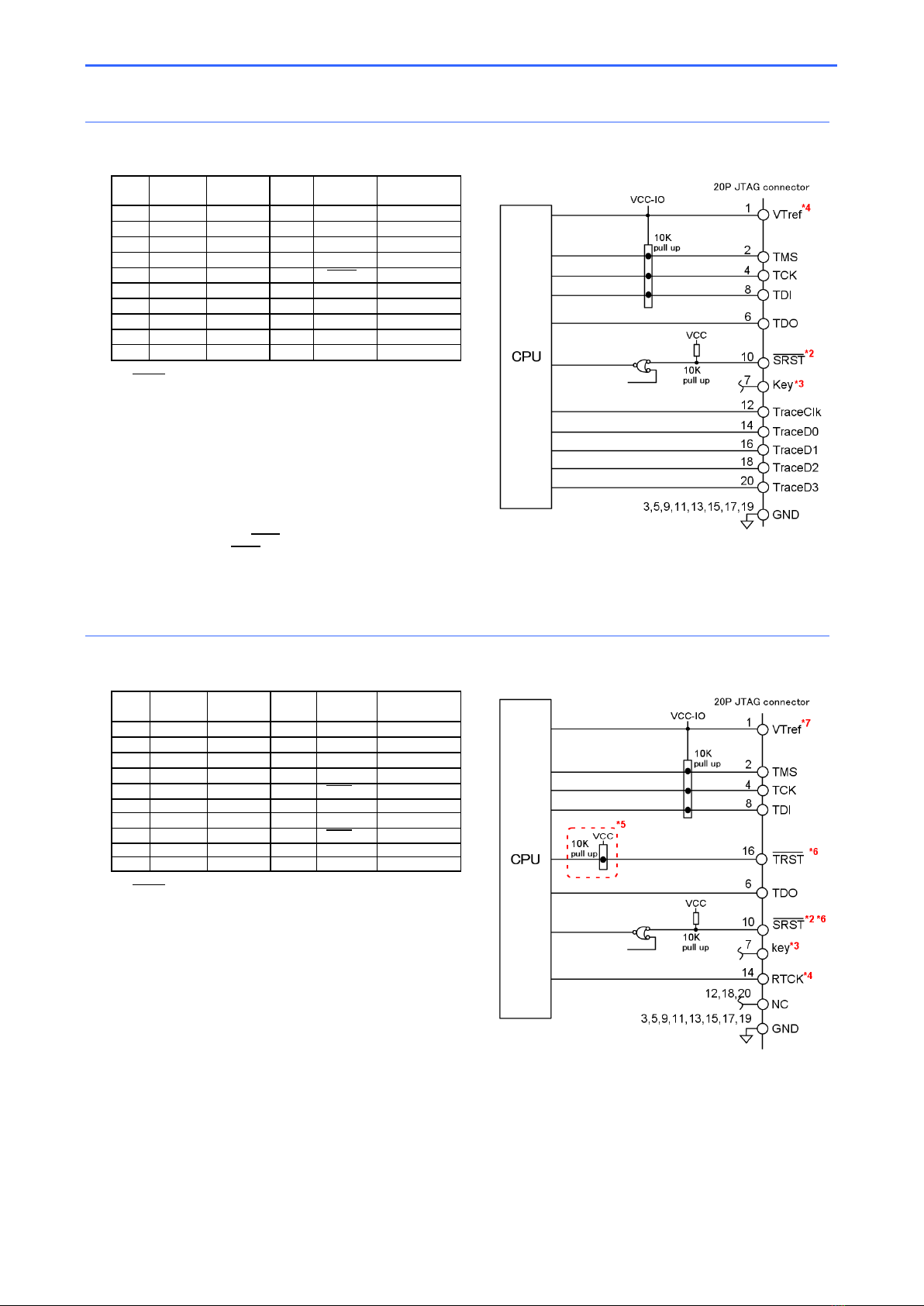
This interface does not use TRST. If the target CPU has a TRST pin, connect a pull up resistor of 10K ohm.
Keep the length of wirings from CPU to the target connector as short as possible. Otherwise, it could contribute to malfunction.
②
JTAG interface
Signals
Target connection reference diagram
Pin
No.
Signal
Input/
Output
*1
Pin
No.
Signal
Input/
Output
*1
1
VTref*8
Output
2
Reserve*5
3
TRST
*6 *7
Input
4
GND
5
TDI
Input
6
GND
7
TMS
Input
8
GND
9
TCK
Input
10
GND
11
RTCK*2
Output
12
GND
13
TDO
Output
14
GND
15
SRST*3 *7
Input
16
GND
17
DBGRQ*4
Input
18
Reserve*9
19
DBGACK*4
Output
20
Reserve*9
*1: The target system side is taken as reference for Input/output.
*2: Leave unconnected if this signal is not present on the CPU or if RTCK
signal is not used.
*3: SRST is an open drain output signal.
Establish wired-OR connection to "power-on-reset" or "system reset"
on the target system, or if wired-OR circuit is not available, connect with
OR circuit. Connect VCC to a power supply that is less than 5V and
matches the circuit of the target system.
*4: Leave unconnected if this signal is not present on the CPU.
*5: Not used by our debugger; leave it as NC.
*6: In some CPUs, a pulldown many be necessary. Refer the CPU
datasheet and make the necessary pull up/pull down changes if
required.
*7: Some precautions are needed for few CPUs made by Renesas
Electronics. Refer [Reference:RZ/A and RZ/T series /SRST, /TRST
reference diagram]for more information.
*8: Connect to the I/O power supply of the CPU JTAG signal.
*9:"Reserve" signal(s) on the debugger could be connected to GND on the
target system.
Keep the length of wirings from CPU to the target connector as short as possible. Otherwise, it could contribute to malfunction.

Technical Information on JTAG / SWD / SWV / ETM ARM-related Target Interface Jan. 27, 2022 (Eighth Edition)
7
■
20-pin 1.27mm-pitch connector
Target connector specifications
(Top view on the target board)
Recommended connector
Manufacturer: Samtec, Inc.
Model: FTSH-110-01-L-DV-K
(For detailed dimensions of the connector, refer to the documentation by manufacturer of the connector.)
*Please look at the pin configuration diagram above and make sure that the connector
is in the right direction before connecting.
Please check the pin number in the signal table above and make sure the signal and the pin
numbers match.
③
SWD interface
Signals
Pin
No.
Signal
Input/
Output
*1
Pin
No.
Signal
Input/
Output
*1
1
VTref*5
Output
2
SWDIO
Input/Output
3
GND
4
SWCLK
Input
5
GND
6
SWO*4
Output
7
Key*3
8
NC
9
GND
10
SRST*2
Input
11
GND
12
NC
13
GND
14
NC
15
GND
16
NC
17
GND
18
NC
19
GND
20
NC
*1: The target system side is taken as reference for Input/output.
*2: SRST is an open drain output signal.
Establish wired-OR connection to "power-on-reset" or "system
reset" on the target system, or if wired-OR circuit is not available,
connect with OR circuit. Connect VCC to a power supply that is
less than 5V and matches the circuit of the target system.
*3: "Key" is intended for protection against wrong insertion.
*4: If the SWV(Serial Wire Viewer) is not used for debugging or the
CPU does not support the SWV, do not connect anything to the
SWO signal.
*5: Connect to the I/O power supply of the CPU SWD signal.
Target connection reference diagram
This interface does not use TRST. If the target CPU has a TRST pin, connect a pull up resistor of 10K ohm.
Keep the length of wirings from CPU to the target connector as short as possible. Otherwise, it could contribute to malfunction.
④
SWD interface + Trace
Signals
Pin
No.
Signal
Input/
Output
*1
Pin
No.
Signal
Input/
Output
*1
1
VTref*6
Output
2
SWDIO
Input/Output
3
GND
4
SWCLK
Input
5
GND
6
SWO*2
Output
7
Key*5
8
NC
Input
9
GND
10
SRST*3
Input
11
GND
12
TraceClk
Output
13
GND
14
TraceD0/SWO*4
Output
15
GND
16
TraceD1
Output
17
GND
18
TraceD2
Output
19
GND
20
TraceD3
Output
*1: The target system side is taken as reference for Input/output.
*2: Connect the signal dedicated to SWO. If pin 14 is used as SWO signal
(refer
*4
), this can be left unconnected.
*3: SRST is an open drain output signal.
Establish wired-OR connection to "power-on-reset" or "system reset"
on the target system, or if wired-OR circuit is not available, connect
with OR circuit. Connect VCC to a power supply that is less than 5V
and matches the circuit of the target system.
*4: In some CPUs, SWO and TraceD0 are multiplexed.
In the case of such pin, connect SWO signal not to Pin No. 6 but to Pin
No.14 even when you intend to use Pin No. 14 as SWO, not as
TraceD0.
*5: "Key" is intended for protection against wrong insertion.
*6: Connect to the I/O power supply of the CPU SWD signal.
Target connection reference diagram
This interface does not use TRST.
If the target CPU has a TRST pin, connect a pull up resistor of 10K ohm.
Keep the length of wirings from CPU to the target connector as short as possible. Otherwise, it could contribute to malfunction.
When using Trace interface, refer chw585_p4_etmtrace_if.pdf.

Technical Information on JTAG / SWD / SWV / ETM ARM-related Target Interface Jan. 27, 2022 (Eighth Edition)
8
⑤
JTAG interface + Trace
Signals
Pin
No.
Signal
Input/
Output
*1
Pin
No.
Signal
Input/
Output
*1
1
VTref*4
Output
2
TMS
Input/Output
3
GND
4
TCK
Input
5
GND
6
TDO
Output
7
Key*3
8
TDI
Input
9
GND
10
SRST*2
Input
11
GND
12
TraceClk
Output
13
GND
14
TraceD0
Output
15
GND
16
TraceD1
Output
17
GND
18
TraceD2
Output
19
GND
20
TraceD3
Output
*1: The target system side is taken as reference for Input/output.
*2: SRST is an open drain output signal.
Establish wired-OR connection to "power-on-reset" or "system reset"
on the target system, or if wired-OR circuit is not available, connect
with OR circuit. Connect VCC to a power supply that is less than 5V
and matches the circuit of the target system.
*3: "Key" is intended for protection against wrong insertion.
*4
: Connect to the I/O power supply of the CPU JTAG signal.
Target connection reference diagram
This interface does not use TRST.
If the target CPU has a TRST pin, connect a pull up resistor of 10K ohm.
Keep the length of wirings from CPU to the target connector as short as possible. Otherwise, it could contribute to malfunction.
When using Trace interface, refer chw585_p4_etmtrace_if.pdf.
⑥
JTAG interface
Signals
Pin
No.
Signal
Input/
Output
*1
Pin
No.
Signal
Input/
Output
*1
1
VTref*7
Output
2
TMS
Input/Output
3
GND
4
TCK
Input
5
GND
6
TDO
Output
7
Key
*3
8
TDI
Input
9
GND
10
SRST*2 *6
Input
11
GND
12
NC
13
GND
14
RTCK*4
Output
15
GND
16
TRST*5 *6
Input
17
GND
18
NC
19
GND
20
NC
*1: The target system side is taken as reference for Input/output.
*2: SRST is an open drain output signal.
Establish wired-OR connection to "power-on-reset" or "system reset"
on the target system, or if wired-OR circuit is not available, connect
with OR circuit. Connect VCC to a power supply that is less than 5V
and matches the circuit of the target system.
*3: "Key" is intended for protection against wrong insertion.
*4: NC If the CPU pin is not present or if RTCK is not used.
*5: In some CPUs, a pulldown many be necessary. Refer the CPU
datasheet and make the necessary pull up/pull down changes if
required.
*6: Some precautions are needed for few CPUs made by Renesas
Electronics. Refer [Reference:RZ/A and RZ/T series /SRST, /TRST
reference diagram]for more information.
*7
:
Connect to the I/O power supply of the CPU JTAG signal.
Target connection reference diagram
Keep the length of wirings from CPU to the target connector as short as possible. Otherwise, it could contribute to malfunction.

Technical Information on JTAG / SWD / SWV / ETM ARM-related Target Interface Jan. 27, 2022 (Eighth Edition)
9
■
10-pin 1.27mm-pitch connector
Target connector specifications
(Top view on the target board)
Recommended connector
Manufacturer:Samtec, Inc.
Model: FTSH-105-01-L-DV-K
(For detailed dimensions of the connector, refer to the documentation by manufacturer of the connector.)
*Please look at the pin configuration diagram above and make sure that the connector
is in the right direction before connecting.
Please check the pin number in the signal table above and make sure the signal and the pin
numbers match.
⑦
SWD interface
Signals
Pin
No.
Signal
Input/
Output
*1
Pin
No.
Signal
Input/
Output
*1
1
VTref*5
Output
2
SWDIO
Input/Output
3
GND
4
SWCLK
Input
5
GND
6
SWO*4
Output
7
Key*3
8
NC
Input
9
GND
10
SRST*2
Input
*1: The target system side is taken as reference for Input/output.
*2: SRST is an open drain output signal.
Establish wired-OR connection to "power-on-reset" or "system
reset" on the target system, or if wired-OR circuit is not available,
connect with OR circuit. Connect VCC to a power supply that is
less than 5V and matches the circuit of the target system.
*3: "Key" is intended for protection against wrong insertion.
*4: If the SWV(Serial Wire Viewer) is not used for debugging or the
CPU does not support the SWV, do not connect anything to the
SWO signal.
*5: Connect to the I/O power supply of the CPU SWD signal.
Target connection reference diagram
This interface does not use TRST.
If the target CPU has a TRST pin, connect a pull up resistor of 10K ohm.
Keep the length of wirings from CPU to the target connector as short as possible. Otherwise, it could contribute to malfunction.
⑧
JTAG interface
Signals
Pin
No.
Signal
Input/
Output
*1
Pin
No.
Signal
Input/
Output
*1
1
VTref*4
Output
2
TMS
Input/Output
3
GND
4
TCK
Input
5
GND
6
TDO
Output
7
Key*3
8
TDI
Input
9
GND
10
SRST*2
Input
*1: The target system side is taken as reference for Input/output.
*2: SRST is an open drain output signal.
Establish wired-OR connection to "power-on-reset" or "system reset"
on the target system, or if wired-OR circuit is not available, connect
with OR circuit. Connect VCC to a power supply that is less than 5V
and matches the circuit of the target system.
*3: "Key" is intended for protection against wrong insertion.
*4: Connect to the I/O power supply of the CPU SWD signal.
Target connection reference diagram
Keep the length of wirings from CPU to the target connector as short as possible. Otherwise, it could contribute to malfunction.

Technical Information on JTAG / SWD / SWV / ETM ARM-related Target Interface Jan. 27, 2022 (Eighth Edition)
10
■
38-pin Mictor connector
Target connector specifications
(Top view on the target board)
Recommended connector
Manufacturer :AMP
Model : Mictor connector
2-767004-2 / 767054-1 / 767061
In mounting ETM connector, place it to the position as close as
possible to CPU so that wiring pattern length will be minimized.
Also in mounting JTAG connector, place it to the position close to
ETM connector.
In addition, you will need to
connect the Grand Bus
Leads of ETM connector to
the GND.
(For detailed dimensions of the connector, refer to the documentation by manufacturer of the connector.)
*Please look at the pin configuration diagram above and make sure that the connector is in the right
direction before connecting.
Please check the pin number in the signal table above and make sure the signal and the pin numbers
match.
⑨
JTAG interface + ETM / PTM
Signals
Pin
No.
Signal
Input/
Output
*1
Pin
No.
Signal
Input/
Output
*1
1
NC
2
NC
3
NC
4
NC
5
GND
6
TRACECLK
Output
7
DBGRQ*2
Input
8
DBGACK*2
Output
9
SRST*3*8
Input
10
Reserve
Input
11
TDO
Output
12
VTref4
Output
13
RTCK*5
Output
14
TVDD*6
Output
15
TCK
Input
16
TRACEDATA[7] *9
Output
17
TMS
Input
18
TRACEDATA[6] *9
Output
19
TDI
Input
20
TRACEDATA[5] *9
Output
21
TRST*7*8
Input
22
TRACEDATA[4] *9
Output
23
Reserve
24
TRACEDATA[3] *9
Output
25
Reserve
26
TRACEDATA[2] *9
Output
27
Reserve
28
TRACEDATA[1] *9
Output
29
Reserve
30
Reserve
Output
31
Reserve
32
Reserve
Output
33
Reserve
34
Reserve
Output
35
Reserve
36
TRACECTL
Output
37
Reserve
38
TRACEDATA[0] *9
Output
*1: The target system side is taken as reference for Input/output.
*2: Leave unconnected if this signal is not present on the CPU.
*3: SRST is an open drain output signal.
Establish wired-OR connection to "power-on-reset" or "system reset" on the
target system, or if wired-OR circuit is not available, connect with OR circuit.
Connect VCC to a power supply that is less than 5V and matches the circuit of
the target system.
*4: Connect to the I/O power supply of the CPU JTAG signal.
*5: Leave unconnected if this signal is not present on the CPU or if RTCK signal is
not used.
*6: Not used by our debugger; leave it as NC.
*7: In some CPUs, a pulldown many be necessary. Refer the CPU datasheet and
make the necessary pull up/pull down changes if required.
*8: Some precautions are needed for few CPUs made by Renesas Electronics.
Refer [Reference:RZ/A and RZ/T series /SRST, /TRST reference diagram]for
more information.
*9: For the names of signals corresponding to respective pin No., see the table of
Signals.
Target connection reference diagram
Keep the length of wirings from CPU to the target connector as short as possible. Otherwise, it could contribute to malfunction.
When using Trace interface, refer chw585_p4_etmtrace_if.pdf.

Technical Information on JTAG / SWD / SWV / ETM ARM-related Target Interface Jan. 27, 2022 (Eighth Edition)
11
⑩
SWD interface + Trace
Signals
Pin
No.
Signal
Input/
Output
*1
Pin
No.
Signal
Input/
Output
*1
1
NC
2
NC
3
NC
4
NC
5
GND
6
TRACECLK
Output
7
Reserve
8
Reserve
9
SRST*2
Input
10
Reserve
11
SWO*4
Output
12
VTref*5
Output
13
Reserve
14
TVDD *3
Output
15
SWCLK
Input
16
TRACEDATA[7]
Output
17
SWDIO
Input/Output
18
TRACEDATA[6]
Output
19
Reserve
20
TRACEDATA[5]
Output
21
Reserve
22
TRACEDATA[4]
Output
23
Reserve
24
TRACEDATA[3]
Output
25
Reserve
26
TRACEDATA[2]
Output
27
Reserve
28
TRACEDATA[1]
Output
29
Reserve
30
Reserve
31
Reserve
32
Reserve
33
Reserve
34
Reserve
35
Reserve
36
Reserve
37
Reserve
38
TRACEDATA[0]
Output
*1: The target system side is taken as reference for Input/output.
*2: SRST is an open drain output signal.
Establish wired-OR connection to "power-on-reset" or "system reset" on the
target system, or if wired-OR circuit is not available, connect with OR circuit.
Connect VCC to a power supply that is less than 5V and matches the circuit
of the target system.
*3: Not used by our debugger; leave it as NC.
*4: If the SWV(Serial Wire Viewer) is not used for debugging or the CPU does not
support the SWV, do not connect anything to the SWO signal.
*5: Connect to the I/O power supply of the CPU SWD signal.
Target connection reference diagram
This interface does not use TRST.
If the target CPU has a TRST pin, connect a pull up resistor of 10K ohm.
Keep the length of wirings from CPU to the target connector as short as possible. Otherwise, it could contribute to malfunction.
When using Trace interface, refer chw585_p4_etmtrace_if.pdf.

Technical Information on JTAG / SWD / SWV / ETM ARM-related Target Interface Jan. 27, 2022 (Eighth Edition)
12
Reference
:
RZ/A and RZ/T series /SRST, /TRST reference diagram
It may be required to control the RES and TRST CPU pins so that they are in low state at power on. Refer the
CPU datasheet for details.

Technical Information on JTAG / SWD / SWV / ETM ARM-related Target Interface Jan. 27, 2022 (Eighth Edition)
Technical Information on JTAG / SWD / SWV / ETM ARM-related Target Interface (Eighth Edition)
Go through the required procedures as stated under Foreign Exchange and Foreign Trade Control Law in exporting (including the case where
travellers directly carry) this product or providing this product for residents outside Japan.
No part of this manual, whether in whole or in part, may be adapted, copied or reproduced without prior permission.
The content of and the specifications of this product are subject to change without prior notice.
Computex Co., Ltd. shall not be held liable for any loss or damage arising from the use of this product although all possible measures have been
taken by Computex Co., Ltd. in good faith to ensure the quality of the product.
Contact us for any questions, feedback, comments, requests or anything of concern to you (or in the event of malfunction) regarding this product or
misprinting or missing information within this manual.
Other names of CPUs etc. mentioned in this manual are trademarks or registered trademarks of their respective manufacturers.
PALMiCE and COMPUTEX are registered trademarks of Computex Co., Ltd. in Japan.

PALMiCE4
Hardware Manual
(Eighth Edition)
Copyright (C)2021 Computex Co., Ltd.

Precautions for use
Read the following thoroughly before attempting to use the product.
In the event of exporting the product (including taking it outside of Japan) or supplying the software to
third parties not residing in Japan, make sure that all procedures as stipulated by the Foreign Exchange
and Foreign Trade Act are strictly observed.
The product, the product manual and the software may not be used or reproduced in whole or in part
without prior permission.
Product details and specifications are subject to modification without prior notice for the purpose of
improving reliability, functionality and design.
Note that although a great deal of care has been taken in manufacturing the product, the company does
not guarantee the results of its use.
The product has been manufactured with no intention of it being used for any purpose that requires
extremely high levels of reliability and safety in functions and performance (such as in military equipment,
nuclear power equipment, aerodynamic or space exploration equipment, traffic equipment, incinerator
control equipment, medical equipment, power generation control equipment, equipment installed on the
seabed, safety devices or similar equipment) in which malfunctions or incorrect operations may result in
direct threats or damage to human lives or that may result in serious threats to society in general. Note
that the company refutes all responsibility for damages incurred through these uses.
Do not install the product in locations subject to excessive amounts of water, humidity, dust, oily vapor,
etc., as it may result in the outbreak of fire, malfunctions or electric shock. Make sure that the correct
power supply and voltage as listed is used.
All copyrights pertaining to CSIDE are the sole property of Computex Co., Ltd.
CSIDE, PALMiCE, and COMPUTEX are registered trademarks of Computex Co., Ltd., Japan.
All other company names, product names, etc., listed within the product manual are trademarks and
registered trademarks of each individual manufacturer

Table of Contents
Chapter 1 Getting Started............................................................... 1
1.1 Introduction.............................................................................................................................................. 1
1.2 Product Composition ........................................................................................................................ 2
1.2.1 Model-J........................................................................................................................................ 2
1.2.2 Model-T........................................................................................................................................ 3
1.3 Optional products ............................................................................................................................... 5
1.3.1 Conversion probes .............................................................................................................. 5
1.4 Product combination ........................................................................................................................ 6
1.4.1 Overview ..................................................................................................................................... 6
1.4.2 Model-J........................................................................................................................................ 8
Reference case①..................................................................................................................................................................... 8
Reference case②..................................................................................................................................................................... 8
Reference case③..................................................................................................................................................................... 8
Reference case④..................................................................................................................................................................... 9
1.4.3 Model-T.....................................................................................................................................10
Reference case⑤..................................................................................................................................................................10
Reference case⑥..................................................................................................................................................................10
Reference case⑦..................................................................................................................................................................10
Reference case⑧..................................................................................................................................................................11
Reference case⑨..................................................................................................................................................................11
Reference case⑩..................................................................................................................................................................11
Reference case⑪..................................................................................................................................................................12
Chapter 2 PALMiCE4 Hardware Specifications............13
2.1 PALMiCE4 specifications............................................................................................................13
2.1.1 About Vbus ...........................................................................................................................14
2.2 PALMiCE4 - parts explained ...................................................................................................15
2.2.1 PALMiCE4 unit....................................................................................................................15
2.2.2 Model-J.....................................................................................................................................16
2.2.3 Model-T.....................................................................................................................................16
2.2.4 Hardware revision.............................................................................................................17
How to read revision sticker ..................................................................................................................................................17
2.3 Probe and cables..............................................................................................................................18

2.3.1 Mictor probe [Model-T] ................................................................................................18
2.3.2 JTAG cable [Model-J] [Model-T].........................................................................19
2.3.3 External probe [Model-J] [Model-T] ..................................................................19
2.3.4 Analyzer probe [Model-T] ..........................................................................................21
2.3.5 JTAG conversion probe [Model-T].....................................................................22
2.3.6 Mictor conversion adapter-20P [Model-T]...................................................22
Chapter 3 Target Interface Specifications ........................23
3.1 Introduction...........................................................................................................................................23
3.2 Model-J specifications ..................................................................................................................23
3.2.1 Shape of the connector for debugger..............................................................23
3.2.2 Dimension of the JTAG cable..................................................................................23
3.2.3 Specifications of target interface signals ........................................................23
3.2.4 The target interface on PALMiCE4 side..........................................................24
3.3 Model-T specifications..................................................................................................................25
3.3.1 Shape of the connector for debugger
(38-pin Mictor connector) ..............................25
3.3.2 Shape of the connector for debugger
(20-pin 1.27mm-pitch connector)...........25
3.3.3 Dimensions of the Mictor probe .............................................................................26
3.3.4 Dimensions of the ADP-P4-MIC38-20HP-CN adapter......................26
3.3.5 Specifications of the target interface signals...............................................27
3.3.6 38 Pin Mictor connector signal table.................................................................28
3.3.7 20 Pin 1.27mm pitch connector signal table..............................................29

PALMiCE4 Hardware Manual Chapter 1 Getting Started 1
Chapter 1
Getting Started
1.1
Introduction
This document explains PALMiCE4 hardware specifications. Refer the User's manual for details on software specifications.
PALMiCE4 ARM is available in two models. Model-J that is specialized for JTAG debugging, and Model-T which is a highly
functional model that incorporates Trace function along with JTAG debugging. Both models have a palm-sized compact design.
USB is used for interfacing with a PC, so no power supply is needed (Vbus compatible*1). This makes PALMiCE4 the ideal
debugging tool and easy to carry around with a laptop while debugging or on a business trip.
Model-J :JTAG debugger
Model-T :JTAG debugger with trace function
As the next advanced version of PALMiCE3, PALMiCE4 series come with a new Real-time monitor function. In addition,
Model-T is equipped with Trace function that provides a more complete debugging environment.
Main features of PALMiCE4 ARM:
【
Model-J / Model-T common features
】
Supports almost all ARM core processors available in the market
JTAG / SWD / SWV debug interfaces supported
Supports CoreSight on-chip debugging/tracing technology
Real-time monitor function
Supports both internal and external flash memory
USB 3.0 compatible, supports super speed, high speed, full speed
No external power supply needed(Vbus compatible*1)
Instant connection to the host PC and the target board
Palm-sized, light, and compact body
【
Model-T specific features
】
Built-in 4GB trace memory
Supported debug interface: JTAG / SWD / SWV / ETM / PTM
*1: Refer ”2.1.1 About Vbus” for more information
Real-time monitor function allows reading and modifying memory contents and
performing debugging without stopping CPU execution. The real-time values of
variables at regular intervals are displayed on a graph.
NOTE
This manual suits for next models
5
Table of contents
Other Computex Recording Equipment manuals