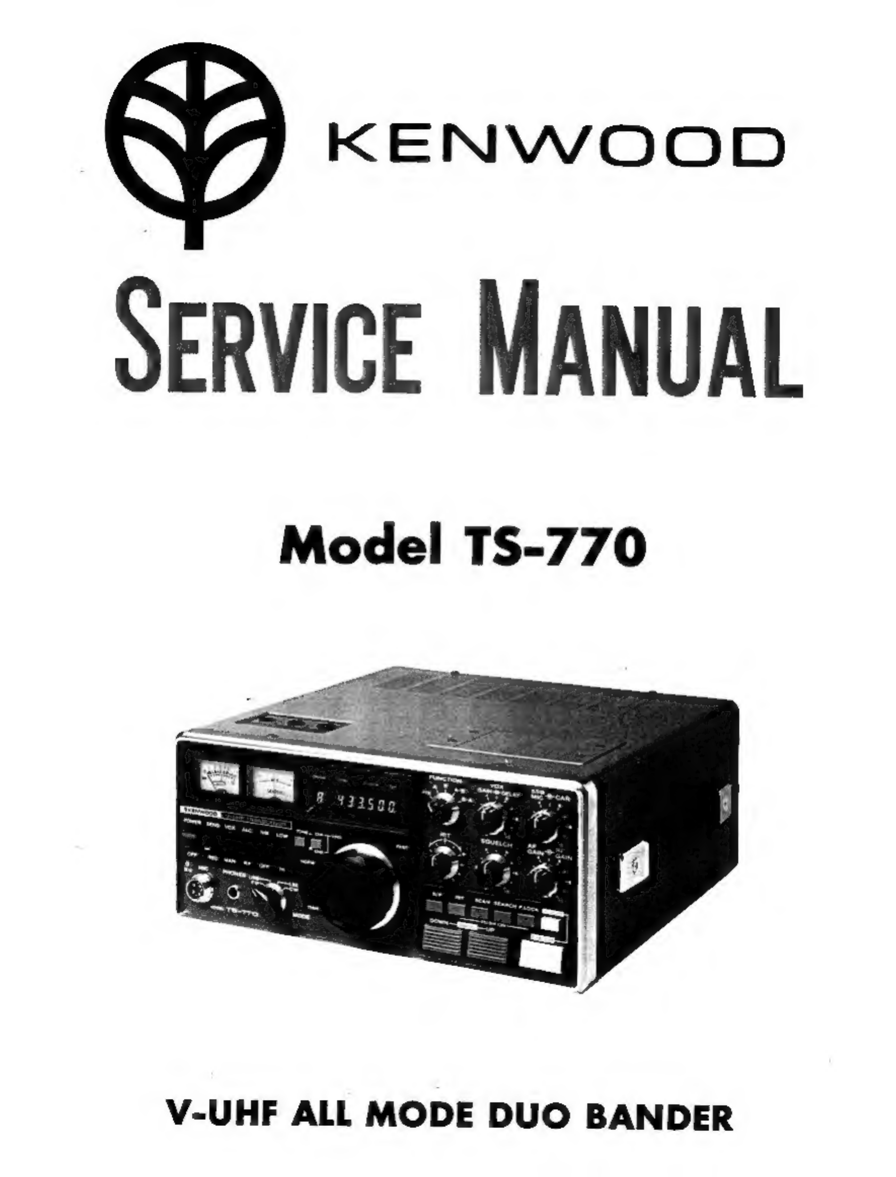
Kenwood TS-770 User manual
Other Kenwood Transceiver manuals

Kenwood
Kenwood TS-5700 User manual

Kenwood
Kenwood TS-450S User manual

Kenwood
Kenwood NEXEDGE NX-220 User manual

Kenwood
Kenwood Nexedge NX-720H User manual

Kenwood
Kenwood TR-2400 User manual

Kenwood
Kenwood TM-471A User manual

Kenwood
Kenwood TK-3202L User manual

Kenwood
Kenwood NX-3720 User manual

Kenwood
Kenwood TK-2317 M3 User manual

Kenwood
Kenwood TK-90 User manual

Kenwood
Kenwood TS-711A User manual

Kenwood
Kenwood TM-732A User manual

Kenwood
Kenwood TK-785 User manual

Kenwood
Kenwood TM-221A User manual

Kenwood
Kenwood TH-F6A User manual

Kenwood
Kenwood TM-231A User manual

Kenwood
Kenwood TK-5410 User manual

Kenwood
Kenwood TK-2160 User manual

Kenwood
Kenwood TM-401B User manual

Kenwood
Kenwood TK-2402V User manual