Crown 800 CSL User manual

Power Base-2 & 800CSL Amplifier Service Manual
1
POWER BASE-2®& 800CSL™
POWER AMPLIFIER
SERVICE MANUAL
K-SVCPB2
1-95
CSL™is a trademark and Power Base-2,®ODEP,® and Crown®are registered trademarks of Crown International, Inc.
MailingAddress:
P.O. Box 1000
Elkhart,INU.S.A. 46515-1000
ShippingAddress:
57620C.R.105
Elkhart, IN U.S.A. 46517
©1995 by CROWN INTERNATIONAL, INC.

Power Base-2 & 800CSL Amplifier Service Manual
2
À PRÉVENIR LE CHOC
ÉLECTRIQUE N’ENLEVEZ
PAS LES COUVERTURES.
RIEN DES PARTIES
UTILES À L’INTÉRIEUR.
DÉBRANCHER LA BORNE
AVANT D’OUVRIR LA
MODULE EN ARRIÈRE.
TO PREVENT ELECTRIC SHOCK DO
NOT REMOVE TOP OR BOTTOM
COVERS. NO USER SERVICEABLE
PARTS INSIDE. REFER SERVICING
TO QUALIFIED SERVICE
PERSONNEL. DISCONNECT
POWER CORD BEFORE REMOVING
REAR INPUT MODULE TO ACCESS
GAIN SWITCH.
CAUTION AVIS
WARNING
TO REDUCE THE RISK OF ELECTRIC
SHOCK, DO NOT EXPOSE THIS
EQUIPMENT TO RAIN OR MOISTURE!
The information furnished in this manual does not include all of the details of design, production, or variations
of the equipment. Nor does it cover every possible situation which may arise during installation, operation or
maintenance. If you need special assistance beyond the scope of this manual, please contact the Crown
Technical Support Group.
Mail: P.O. Box 1000 Elkhart IN 46515-1000
Shipping: 57620 C.R. 105 Elkhart IN 46517
Phone: (800) 342-6939/(219) 294-8200
FAX: (219) 294-8301

Power Base-2 & 800CSL Amplifier Service Manual
3
Introduction .............................................................4
Scope......................................................................4
Warranty..................................................................4
Parts ........................................................................5
Specifications..........................................................6
Voltage Conversion .................................................7
Circuit Theory ..........................................................8
Test Procedures....................................................13
Mechanical Parts Listing .......................................17
Module Information ...............................................20
Q42647-0 Output Module (MT/MA) ......................21
Q42717-1 Output Module (MT/MA #2)..................22
Q42871-6 Output Module (TO-3P MT/MA) ...........23
Q42966-4 Output Module (TO-3P #2)...................24
Q43015-9 Output Module (THC)...........................25
Q43203-1 Output Module (THC #2)......................26
Q42665-2 Main Module (Original).........................27
Q42683-5 Main Module (#2) .................................29
Q42818-3 Main Module (3rd Gain) .......................31
Q43059-7 Main Module (THC) ..............................34
Table of Contents

Power Base-2 & 800CSL Amplifier Service Manual
4
Crown
Technical Support Group
Factory Service
Parts Department
Mailing Address:
PO Box 1000
Elkhart, IN USA 46515-1000
Shipping Address:
57620 C.R. 105
Elkhart, IN USA 46517
Phone: (219) 294-8200
Toll Free: (800) 342-6939
FAX: (219) 294-8301
This manual contains service information on Crown
poweramplifiers. Itisdesignedtobeusedinconjunc-
tion with the applicable Owner's Manual. However,
some important information is duplicated in this Ser-
viceManual incasethe Owner'sManual is not readily
available.
NOTE: THE INFORMATION IN THIS MANUAL IS INTENDED
FOR USE BY AN EXPERIENCED TECHNICIAN ONLY!
SCOPE
ThisService Manualincludes several sections. These
sections include Parts Ordering, Specifications, Volt-
age Conversion, Circuit Theory, Factory Test Proce-
dures,MechanicalPartsLists,andModulePartsLists.
Schematics are attached. Note that component parts
withcircuitboardcomprise a completemodule.Mod-
ule part numbers are always associated with a spe-
cific circuit board, although an unpopulated circuit
board may be built up with different parts to create
differentmodules.NotethatCrowndoesnotsellblank
(unpopulated) circuit boards.
Each of the compact audio power amplifiers are
designed for professional or commercial use. Provid-
inghigh power amplification from 20Hz to 20KHzwith
minimumdistortion, they featurebalanced inputs with
bridged and parallel monophonic capability. Specific
features vary depending on model family.
WARRANTY
Each Owner's Manual contains basic policies as re-
lated to the customer. In addition it should be stated
that this service documentation is meant to be used
only by properly trained service personnel. Because
most Crown products carry a 3 Year Full Warranty
(includingroundtripshippingwithintheUnitedStates),
all warranty service should be referred to the Crown
Factory or Authorized Warranty Service Center. See
theapplicableOwner’sManualforwarrantydetails.To
find the location of the nearest Authorized Service
Centeror obtaininstructions for receiving Crown Fac-
toryServicepleasecontacttheCrown Technical Sup-
port Group (within North America) or your Crown/
Amcron Importer (outside North America).
Introduction

Power Base-2 & 800CSL Amplifier Service Manual
5
Parts
shipmentonaC.O.D.orpre-payment(checkorcredit
card) basis.
TERMS
Normal terms are pre-paid. Net-30 Days applies to
onlythosefirmshavingpre-establishedaccountswith
Crown. If pre-paying, the order must be packed and
weighed before a total bill can be established, after
which an amount due will be issued and shipment
made upon receipt of pre-payment. New parts re-
turned for credit are subject to a 10% re-stocking fee,
and authorization from the Crown Parts Department
must be obtained before returning parts for credit.
Crownisnotageneral parts warehouse. Partssoldby
the Crown Parts Department are solely for servicing
Crown/Amcron products. Part prices and availabil-
ity are subject to change without notice.
GENERAL INFORMATION
Latersectionsincludebothmechanical and electrical
parts lists for this product. The parts listed are current
as of the date printed. Crown reserves the right to
modify and improve its products for the benefit of its
customers.
PART NUMBERING SYSTEMS
As of the printing of this manual, Crown is using two
numbering systems. The elder system always uses
eight characters. The first character is a letter. Com-
monlettersusedareC,D,H,M,P, andQ.Thesecond
through sixth characters are numbers. The numbers
build sequentially (for each prefix letter) as new parts
are added to our parts inventory system. (In some
cases there will be a space then a four character
numberafterthe prefix letter;thespace is considered
a character.) The seventh character is usually a hy-
phen,thoughitmaybe a lettertoindicatearevisionor
specialnote.Thelastcharacteriscalledacheck-digit,
and is useful to Crown for internal tracking.
Crown is in the process of converting to a new part
number system. Length may vary from eight to twelve
characters. There is still a letter prefix, then five
numbers. These five numbers identify a type of part.
The seventh character is a hyphen. Remaining char-
acters identify the details of the type of part identified
by the first part of the number.
STANDARD AND SPECIAL PARTS
Many smaller electrical and electronic parts used by
Crown are stocked by and available from electronic
supply houses. However, some electronic parts that
appear to be standard are actually special. A part
ordered from Crown will assure an acceptable re-
placement. Structural items such as modules and
panels are available from Crown only.
ORDERING PARTS
When ordering parts, be sure to give the product
model, and include a description and part number
(CPN/DPN) from the parts listing. Price quotes are
available on request.
SHIPMENT
Shipment will be normally made by UPS or best other
method unless you specify otherwise. Shipments are
made to and from Elkhart, Indiana USA, only. Estab-
lished accounts with Crown will receive shipment
freightprepaidandwillbebilled.Allotherswillreceive
Crown
Parts Department
Mailing Address:
PO Box 1000
Elkhart, IN USA 46515-1000
Shipping Address:
57620 C.R. 105
Elkhart, IN USA 46517
Phone: (219) 294-8210
or: (219) 294-8211
Toll Free: (800) 342-6939
FAX: (219) 294-8301

Power Base-2 & 800CSL Amplifier Service Manual
6
Specifications
Unless noted otherwise, all specifications are based
on driving an 8 ohm load per channel, both channels
driven, the sensitivity switch in the 26dB position, the
AC supply is 120VAC at 60Hz. Crown specifications
areguaranteed throughthe warranty period(normally
3years). Becauseour testing methods are morestrin-
gent than our published specifications, every Crown
amplifier will exceed its published specifications.
POWER
Power
8 Ohm Stereo—320W/Ch
4 Ohm Stereo—400W/Ch
8 Ohm Bridge Mono—965W
4 Ohm Parallel Mono—680W
2 Ohm Parallel Mono—955W
Load Impedances: Rated for 16, 8, 4, and 2 (parallel
monoonly)Ohmoperation;safewithalltypesofloads,
even totally reactive loads.
AC Mains: 120VAC at 60 Hz with standard 3 wire
grounded 15A connector with single voltage trans-
former and fan for North American units; 100VAC,
120VAC, 220VAC, and 240VAC at 50 or 60 Hz when
equipped with universal transformer, applicable fan,
and other applicable hardware with country specific
power cord. Note that at 50 Hz fan speed is reduced.
PERFORMANCE
Frequency Response: ±0.1dB from 20 Hz to 20 kHz at 1
Watt.
Phase Response: ±10° from 10 Hz to 20 kHz at 1 Watt.
Signal to Noise Ratio: Better than 105 dB (A-weighted)
below max. average power from 20 Hz to 20 kHz.
Total Harmonic Distortion (THD): <0.05% from 20 Hz to
1 kHz, increasing linearly to 0.1% at 20 kHz at 170W.
I.M.Distortion:<0.05%from10milliwattsto170Wat26
dB gain.
Slew Rate: >13V per microsecond.
Damping Factor: >1000 from 10 Hz to 400 Hz.
DC Offset: <10 millivolts.
Input Impedance: Nominally 20K ohms balanced; 10K
ohms unbalanced.
Output Impedance: <10 milliohms in series with <2
microhenries.
Protection Systems: Output Device Emulation Protec-
tion (ODEP) limits drive in the event of dangerous
dynamicthermalconditionswithoutinterruptingpower.
Currentlimitingforshortedloadprotection.DC/LFand
common mode output current Fault circuitry to mute
audio.Delayof4secondsfromturnonmutesamplifier
topreventdangerousturn-ontransients.Highvoltage
fusein maintransformer primaryand lowvoltage fuse
in fan primary. Slew rate limiting to prevent RF burn
out.
MECHANICAL
Input Connectors: Balanced 1/4 inch phone jacks.
Output Connectors: Color-coded 5-way binding posts
on 3/4 inch centers; spaced 3/4 inch apart.
Front Panel Controls: A rocker on/off power switch.
Back Panel Controls: A three-position switch which
selects Stereo,Bridge-Mono,orParallel-Monomode;
a two position input ground-lift switch, and level con-
trols for each channel.
InternalControls:Athree-positionswitchselects0.775V,
1.4V, or 26 dB voltage gain input sensitivity (all units
manufactured with D 7911-7 main module or later;
earlier models only allowed for 0.775V or 26 dB gain).
Indicators:RedEnableindicator shows on/offstatusof
low-voltage power supply.
Construction: Black splatter-coat steel chassis with
specially designed flow-through ventilation system.
Mounting: Standard EIA 310 front-panel rack mount
with supports for supplemental rear corner mounting.
Dimensions:19incheswide,3.5incheshigh,16inches
deep behind front mounting surface.
Weight: 32 lbs.

Power Base-2 & 800CSL Amplifier Service Manual
7
Voltage Conversion
Note: The only versions of this
productproducedat the Crown
Factory with international volt-
agecapabilitiesbuilt in areCSL
versions built specifically for
sale outside the United States.
P16
P10 P15
P14
P13
P12
P11
P9
P8
P7
P6
P5
P4
P3
P2
P1
P22
P21
P18 P17
P19
P20
F1F100
BRN
BLU
100V Connections:
P10 to P15
P11 to P14
P7 to P12
120V Connections:
P10 to P16
P11 to P14
P7 to P13
220V Connections:
P10 to P15
P9 to P14
P8 to P13
240V Connections:
P10 to P16
P9 to P14
P8 to P13
For list of applicable
transformer, fuse F100,
fanformer, and power
cord refer to voltage-
parts cross-reference.
S1 Power Switch
PB/CSL Universal Fuse Board
Specific parts are required for the PB-2/800CSL in
order to be used at different international line volt-
ages. Refer also to Mechanical Parts Lists.
100 to 120V AC Mains:
20A Fuse A10285-28
0.5A Low Voltage Supply Fuse A10285-7
Power Transformer (Universal) D 7599-0
Power Transformer (United States) D 6748-4
Transmotor 120V 50 Hz H43338-5
Transmotor 120V 60 Hz H43065-4
220V to 240V AC Mains:
10A Fuse A10285-26
0.5A Low Voltage Supply Fuse A10285-7
Power Transformer D 7599-0
Transmotor 120V 50Hz H43338-5

Power Base-2 & 800CSL Amplifier Service Manual
8
Theory
OVERVIEW
It should be noted from the outset that the PB-1 and
460CSL amplifiers are electrically and mechanically
identical products. The only differences, from a ser-
vice perspective, are cosmetic. For the purposes of
servicing the products, it should also be known that
the CSL version has been on the market since 1992.
SincethePBamplifiershavebeeninproductionsince
the mid-1980’s there are a number of electrical and
mechanicalpartsassociatedwiththeolderPBmodels
only.ItisalsoimportanttorealizethatovertimeCrown
has introduced numerous improvements to PB/CSL
amplifiers. Though often changes are minor, and are
madeforavarietyofreasons,afewchangeshavehad
a significant impact on the operation of the circuitry.
This manual is up to date as of the time of writing. For
additional information regarding these amplifiers, re-
fer to the applicable Technical Notes provided by
Crown for this product.
Thissectionofthemanualexplainsthegeneralopera-
tion of a typical Crown power amplifier. Topics cov-
eredincludeFrontEnd,GroundedBridge,andODEP.
Due to variations in design from vintage to vintage
(andsimilaritieswithotherproductsCrown)thetheory
of operation remains simplified.
FEATURES
Power Base/CSL amplifiers utilize numerous Crown
innovations including grounded bridge and ODEP
technologies. Cooling techniques make use of the
whatisessentiallyairconditionertechnology.Airflows
bottom to top, and front to side. Air flows a short
distance across a wide heatsink. This type of air flow
provides significantly better cooling than the “wind
tunnel” technology used by many other manufactur-
ers.Outputtransistorsareofthemetalcantyperather
thanplastic case. Thisallowsfor asignificantlyhigher
thermal margin for the given voltage and current
ratings. All devices used are tested and graded to
ensure maximum reliability. Another electronic tech-
nique used is negative feedback. Almost all power
amplifiers utilize negative feedback to control gain
and provide stability, but Crown uses multiple nested
feedback loops for maximum stability and greatly
improveddamping.MostCrownamplifiershavedamp-
inginexcessof1000inthebassfrequencyrange.This
feedback, along with our compensation and ultra-low
distortion output topology, make Crown amplifiers
superior.
Features specific to the Power Base/CSL Series’ in-
clude a single core transformer (one primary with two
independentungroundedsecondaries),afulltimefull
speed fan which also serves as the low voltage
transformer, slew rate limiting, and audio muting for
delay or protective action. This amplifier can operate
in either a Bridged or Parallel Mono mode as well as
dual (stereo). A sensitivity switch allows selection of
input voltage required for rated output. Level controls
arerearmounted.Theonlyindicatorprovidedtellsthe
operator that the low voltage supply is energized. In
general, the packaging of this model is designed for
maximum watt/price/weight/size value. It is the most
basic grounded bridge amplifier series now available
from Crown.
Foradditionaldetailsrefertothespecificationsection,
or to the applicable Owner’s Manual.
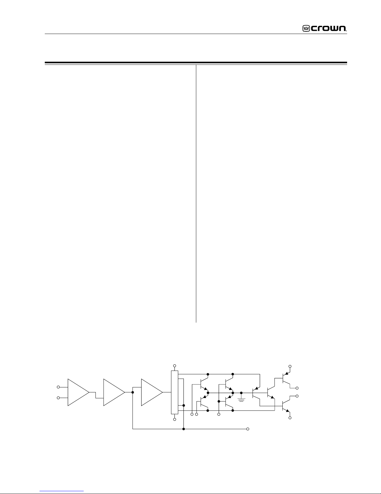
FRONT END OPERATION
Thefront end iscomprised of threestages: Balanced
Gain Stage (BGS), Variable Gain Stage (VGS), and
theError Amp. Figure1 shows asimplified diagram of
a typical front end with voltage amplification stages.
Balanced Gain Stage (BGS)
Input to the amplifier is balanced. The shield may be
isolated from chassis ground by an RC network to
interrupt ground loops (early models did not have the
Ground Lift feature) via the Ground Lift Switch. The
non-inverting (hot) side of the balanced input is fed to
the non-inverting input of the first op-amp stage. The
inverting (negative) side of the balanced input is fed
to the inverting input of the first op-amp stage. A
potentiometerisprovidedforcommonmoderejection
adjustment. Electrically, the BGS is at unity gain.
(From an audio perspective, however, this stage
actually provides +6dB gain if a fully balanced signal
is placed on its input.) The BGS is a non-inverting
stage. It’s output is delivered to the Variable Gain
Stage.
Variable Gain Stage (VGS)
Note: Older models only had two front end stages.
The functions of this stage were combined, primarily,
with those of the third.
FromtheoutputoftheBGS,thesignalgoestotheVGS
where gain is determined by the position of the Sen-
sitivity Switch, and level is determined by the level
control. VGS is an inverting stage with the input being
fedto itsop-amp stage. Because gain after this stage
is fixed at 26dB (factor of 20), greater amplifier sensi-

Power Base-2 & 800CSL Amplifier Service Manual
9
Theory
tivityisachievedbycontrollingtheratiooffeedbackto
input resistance. The Sensitivity Switch sets the input
impedanceto this stage and varies the gainsuch that
the overall amplifier gain is 26 dB, or is adjusted
appropriately for 0.775V or 1.4V input to attain rated
output.Notethatearliermodels(beforemainmodules
built with D 7911-7 board) did not support the 1.4V
sensitivity.
Error Amp
The inverted output from the VGS is fed to the non-
invertinginputoftheErrorAmpop-ampstagethrough
anACcouplingcapacitorandinputresistor.Amplifier
output is fed back via the negative feedback (NFb)
loop resistor. The ratio of feedback resistor to input
resistor fixes gain from the Error Amp input to the
output of the amplifier at 26 dB. Diodes prevent
overdriving the Error Amp. Because the Error Amp
amplifies the difference between input and output
signals, any difference in the two waveforms will
produceanearopenloopgainconditionwhichinturn
results in high peak output voltage. The output of the
Error Amp, called the Error Signal (ES) drives the
Voltage Translators.
VOLTAGE AMPLIFICATION
The Voltage Translator stage separates the output of
the Error Amp into balanced positive and negative
drive voltages for the Last Voltage Amplifiers (LVAs),
translatingthesignalfromground referenced ±15Vto
±Vccreference.LVAsprovidethemainvoltageampli-
fication and drive the High Side output stages. Gain
from Voltage Translator input to amplifier output is a
factor of 25.2.
Voltage Translators
A voltage divider network splits the Error Signal (ES)
into positive and negative drive signals for the bal-
ancedvoltagetranslatorstage.Theseoffsetreference
voltages drive the input to the Voltage Translator
transistors. A nested NFb loop from the output of the
amplifier mixes with the inverted signal riding on the
offsetreferences.Thisnegativefeedbackfixesgainat
theoffset referencepoints (andthe outputof the Error
Amp) at a factor of -25.2 with respect to the amplifier
output. The Voltage Translators are arranged in a
common base configuration for non-inverting voltage
gain with equal gain. They shift the audio from the
±15V reference to VCC reference. Their outputs drive
their respective LVA.
Also tied into the Voltage Translator inputs are ODEP
limiting transistors and control/protection transistors.
The ODEP transistors steal drive as dictated by the
ODEP circuitry (discussed later). The control/protec-
tiontransistorsactasswitchestototallyshuntaudioto
ground during the turn-on delay, or during a DC/LF or
Fault protective action.
Last Voltage Amplifiers (LVAs)
The Voltage Translator stage channels the signal to
the Last Voltage Amplifiers (LVA's) in a balanced
configuration.The+LVAand-LVA,withtheirpush-pull
effect through the Bias Servo, drive the fully comple-
mentary output stage. The LVAs are configured as
common emitter amplifiers. This configuration pro-
videssufficientvoltagegainandinvertstheaudio.The
polarity inversion is necessary to avoid an overall
polarity inversion from input jack to output jack, and it
+
-+
-+
-
BGS VGS Error
Amp
Audio
Inputs
Voltage Divider
NFb Loop
+
-
ODEP Mute
+15V
-15V
+VCC
-VCC
NPN Outputs (+HS)
PNP Outputs (-HS)
Q100
Q103
Q121
Q122
Q101
Q102
Q105
Q110
Voltage
Translators
LVA's
Figure 1. Typical Amplifier Front End and Voltage Amplification Stages.

Power Base-2 & 800CSL Amplifier Service Manual
10
allows the NFb loop to control Error Amp gain by
feedingbacktoitsnon-invertinginput(withitspolarity
opposite to the output of the VGS). With the added
voltage swing provided by the LVAs, the signal then
gains current amplification through the Darlington
emitter-follower output stage.
GROUNDED BRIDGE TOPOLOGY
Figure 2 is a simplified example of the grounded
bridge output topology. It consists of four quadrants
of three deep Darlington (composite) emitter-follower
stages per channel: one NPN and one PNP on the
High Side of the bridge (driving the load), and one
NPN and one PNP on the Low Side of the bridge
(controlling the ground reference for the rails). The
output stages are biased to operate class AB+B for
ultra low distortion in the signal zero-crossing region
and high efficiency.
High Side (HS)
The High Side (HS) of the bridge operates much like
aconventionalbipolarpush-pulloutputconfiguration.
Astheinputdrivevoltagebecomesmorepositive,the
HSNPN conducts and delivers positive voltage tothe
load. Eventually the NPN devices reach full conduc-
tion and +Vcc is across the load. At this time the HS
PNP is biased off. When the drive signal is negative
going,theHSPNPconductstodeliver-Vcctotheload
and the HS NPN stage is off.
Theory
+
-
+Vcc (Positive Rail)
-Vcc (Negative Rail)
Load
(speaker)
Input
signal
HIGH SIDE LOW SIDE
Inverting Op-amp
Figure 2. Crown Patented Grounded Bridge Topology
The output of the +LVA drives the base of predriver
device. Together, the predriver and driver form the
first two parts of the three-deep Darlington and are
biased class AB. They provide output drive through
the bias resistor, bypassing the output devices, at
levelsbelow about100mW. AnRLC networkbetween
the predriver and driver provide phase shift compen-
sation and limit driver base current to safe levels.
Output devices are biased class B, just below cutoff.
Atabout100mWoutputtheyswitchontoconducthigh
currenttotheload.Togetherwithpredriveranddriver,
the output device provide an overall class AB+B
output.
The negative half of the HS is almost identical to the
positive half, except that the devices are PNP. One
difference is that the PNP bias resistor is slighter
greaterin value sothat PNP outputdevices run closer
to the cutoff level under static (no signal) conditions.
This is because PNP devices require greater drive
current.
HS bias is regulated by Q18, the Bias Servo. Q18 is a
Vbe multiplier which maintains approximately 3.3V
Vceunderstaticconditions.Thepositiveandnegative
halves of the HS output are in parallel with this 3.3V.
With a full base-emitter on voltage drop across
predrivers and drivers, the balance of voltage results
inapproximately.35Vdropacrossthebiasresistorsin

Power Base-2 & 800CSL Amplifier Service Manual
11
thepositivehalf,andabout.5Vacrossthebiasresistor
inthenegativehalf.Q18 conduction (and thusbias)is
adjustable.
A diode string prevents excessive charge build up
within the high conduction output devices when off.
Flyback diodes shunt back-EMF pulses from reactive
loads to the power supply to protect output devices
from dangerous reverse voltage levels. An output
terminating circuit blocks RF on output lines from
entering the amplifier through its output connectors.
Low Side (LS)
The Low Side (LS) operates quite differently. The
power supply bridge rectifier is not ground refer-
enced, nor is the secondary of the main transformer.
In other words, the high voltage power supply floats
withrespecttoground,but±Vccremainconstantwith
respecttoeachother.This allows thepowersupplyto
deliver +Vcc and -Vcc from the same bridge rectifier
and filter as a total difference in potential, regardless
of their voltages with respect to ground. The LS uses
inverted feedback from the HS output to control the
ground reference for the rails (±Vcc). Both LS quad-
rantsarearrangedinathree-deepDarlingtonandare
biased AB+B in the same manner as the HS.
Whentheamplifieroutputswingspositive,theaudiois
fed to an op-amp stage where it is inverted. This
invertedsignalisdelivered directly to thebasesofthe
positive(NPN)and negative (PNP)LSpredrivers.The
negative drive forces the LS PNP devices on (NPN
off). As the PNP devices conduct, Vce of the PNP
Darlington drops. With LS device emitters tied to
ground, -Vcc is pulled toward ground reference.
Sincethepowersupplyisnotgroundreferenced(and
the total voltage from +Vcc to -Vcc is constant) +Vcc
is forced higher above ground potential. This contin-
ues until, at the positive amplifier output peak, -Vcc =
0V and +Vcc equals the total power supply potential
with a positive polarity. If, for example, the power
supplyproducedatotalof70Vfromrailtorail(±35VDC
measured from ground with no signal), the amplifier
output would reach a positive peak of +70V.
Conversely, during a negative swing of the HS output
where HS PNP devices conduct, the op-amp would
output a positive voltage forcing LS NPN devices to
conduct. This would result in +Vcc swinging toward
ground potential and -Vcc further from ground poten-
tial. At the negative amplifier output peak, +Vcc = 0V
and -Vcc equals the total power supply potential with
Theory
anegativepolarity.Usingthesameexampleasabove,
a 70V supply would allow a negative output peak of -
70V. In summary, a power supply which produces a
total of 70VDC rail to rail (or ±35VDC statically) is
capableofproducing140Vpeak-to-peakattheampli-
fier output when the grounded bridge topology is
used. The voltage used in this example are relatively
close to the voltages of the PB-1/460CSL.
The total effect is to deliver a peak to peak voltage to
the speaker load which is twice the voltage produced
bythe power supply. Benefits include full utilizationof
the power supply (it conducts current during both
halves of the output signal; conventional designs
require two power supplies per channel, one positive
and one negative), and never exposing any output
device to more than half of the peak to peak output
voltage (which does occur in conventional designs).
Low side bias is established by a diode string which
also shunts built up charges on the output devices.
Bias is adjustable via potentiometer. Flyback diodes
perform the same function as the HS flybacks. The
output of the LS is tied directly to chassis ground via
ground strap.
OUTPUT DEVICE EMULATION PROTECTION
(ODEP)
Tofurtherprotecttheoutputstages,aspeciallydevel-
oped ODEP circuit is used. It produces a complex
analog output signal. This signal is proportional to the
always changing safe-operating-area margin of the
output transistors. The ODEP signal controls the Volt-
age Translator stage by removing drive that may
exceed the safe-operating-area of the output stage.
ODEP senses output current by measuring the volt-
age dropped across LS emitter resistors. LS NPN
current (negative amplifier output) and +Vcc are
sensed,thenmultipliedtoobtainasignalproportional
tooutputpower.PositiveandnegativeODEPvoltages
areadjustableviatwopotentiometers.Across±ODEP
are a PTC and a thermal sense (current source). The
PTC is essentially a cutoff switch that causes hard
ODEP limiting if heatsink temperature exceeds a safe
maximum, regardless of signal level. The thermal
sense causes the differential between +ODEP and –
ODEPtodecreaseasheatsinktemperatureincreases.
Anincreaseinpositiveoutputsignaloutputintoaload
will result in –ODEP voltage dropping; an increase in
negativeoutputvoltageandcurrentwillcause+ODEP
voltage to drop. A complex RC network between the

Power Base-2 & 800CSL Amplifier Service Manual
12
Theory
±ODEP circuitry is used to simulate the thermal barri-
ers between the interior of the output device die
(immeasurable by normal means) and the time delay
fromheat generation at the die until heat dissipates to
the thermal sensor. The combined effects of thermal
history and instantaneous dynamic power level result
in an accurate simulation of the actual thermal condi-
tion of the output transistors.
NEGATIVE
LOW SIDE
OUTPUT
PNP STAGE
POSITIVE
LOW SIDE
OUTPUT
NPN STAGE
NEGATIVE
HIGH SIDE
OUTPUT
PNP STAGE
POSITIVE
HIGH SIDE
OUTPUT
NPN STAGE
HIGH SIDE
BIAS
SERVO
+LVA
-1
-LVA
-1
+VOLTAGE
TRANSLATOR
-VOLTAGE
TRANSLATOR
OUTPUT
DEVICE
EMULATION
PROTECTION
ERROR
AMP
VGSBGS
BALANCED
INPUTS
INVERTING
BRIDGE
BALANCE
LOW SIDE
BIAS
DIODE
STRING
-1
-1
MAIN NEGATIVE FEEDBACK (NFb) LOOP
Figure 3. Typical Crown Amplifier Basic Block Diagram (One Channel Shown)

Power Base-2 & 800CSL Amplifier Service Manual
13
Checkout Procedures
GENERAL INFORMATION
The following test procedures are to be used to verify
operation of this amplifier. DO NOT connect a load or
inject a signal unless directed to do so by the proce-
dure. These tests, though meant for verification and
alignment of the amplifier, may also be very helpful in
troubleshooting. For best results, tests should be
performed in order.
AlltestsassumethatACpowerisfromaregulated120
VAC source. Test equipment includes an oscillo-
scope, a DMM, a signal generator, loads, and I.M.D.
and T.H.D. noise test equipment.
STANDARD INITIAL CONDITIONS
Level controls fully clockwise.
Stereo/Mono switch in Stereo.
Sensitivity switch in 26 dB fixed gain position.
It is assumed, in each step, that conditions of the
amplifier are per these initial conditions unless other-
wise specified.
TEST 1: DC OFFSET
Spec: 0 VDC, ±10 mV.
InitialConditions:Controlsperstandard,inputsshorted.
Procedure: Measure DC voltage at the output connec-
tors (rear panel). There is no adjustment for output
offset.Ifspecisnotmet,thereisanelectricalmalfunc-
tion. Slightly out of spec measurement is usually due
to U104/U204 out of tolorance.
TEST 2: OUTPUT BIAS ADJUSTMENT
Spec: 300 to 320 mVDC.
InitialConditions: Controlsperstandard,heatsinktem-
perature less than 40°C.
Procedure:MeasureDCvoltagesontheoutputmodule
across R02, adjust R26 if necessary. Measure DC
voltagesontheoutputmoduleacrossR21,adjustR23
if necessary. Repeat for second channel.
TEST 3: ODEP VOLTAGE ADJUSTMENT
Spec: Cold Bias Per Charts Below ±0.1V DC.
Initial Conditions: Controls per standard, heatsink at
room temperature 20 to 30°C (68 to 86°F). Note: This
adjustment should normally be performed within 2
minutes of turn on from ambient (cold) conditions. If
possible measure heatsink temperature, if not mea-
sure ambient room temperature. Use this information
when referencing the chart below. The following is a
list of ODEP Bias Voltages VS. Temperature.
°F °C V–ODEP V+ODEP
66 18.9 –10.31 11.41
68 20.0 –10.26 11.36
70 21.1 –10.20 11.30
72 22.2 –10.14 11.24
74 23.3 –10.09 11.19
76 24.4 –10.03 11.13
77 25.0 –10.00 11.10
78 25.6 –9.97 11.07
80 26.7 –9.91 11.01
82 27.8 –9.86 10.96
84 28.9 –9.80 10.90
86 30.0 –9.74 10.84
88 31.1 –9.69 10.79
90 32.2 –9.63 10.73
92 33.3 –9.57 10.67
94 34.4 –9.51 10.61
–ODEP Procedure: Measure pin 6 of U100 and, if
necessary, adjust R121 to obtain V–ODEP as specified
above. Measure pin 6 of U200 and, if necessary,
adjust R221 to obtain V–ODEP as specified above.
+ODEP Procedure: Measure pin 6 of U103 and, if
necessary, adjust R132 to obtain V+ODEP as specified
above. Measure pin 6 of U203 and, if necessary,
adjust R232 to obtain V+ODEP as specified above.

Power Base-2 & 800CSL Amplifier Service Manual
14
TEST 4: AC POWER DRAW
Spec: 90 Watts maximum quiescent.
Initial Conditions: Controls per standard.
Procedure: With no input signal and no load, measure
AC line wattage draw. If current draw is excessive,
check for high AC line voltage or high bias voltage.
TEST 5: COMMON MODE REJECTION
Spec at 100 Hz: –70 dB.
Spec at 20 kHz: –50 dB.
Initial Conditions: Controls per standard.
Procedure: No load. Inject a 0 dBu 100 Hz sine wave
intoeachchannel,onechannelatatime,withinverting
and non-inverting inputs shorted together. At the
output measure less than –44 dBu. Inject a 0 dBu 20
kHz sine wave into each channel, one channel at a
time, with inverting and non-inverting inputs shorted
together. At the output measure less than –24 dBu.
Adjust R921 or R1021, if necessary, to obtain the
required measurements. (In older units the adjust-
ments are done using N100/N200.)
TEST 6: VOLTAGE GAIN
Spec: ±3% when the Sensitivity Switch is set for 26dB
gain,±6%whentheSensitivitySwitchissetfor0.775V
or 1.4V sensitivity.
Initial Conditions: Controls per standard.
Procedure: No load connected. Inject a 0.775 VAC 1
kHz sine wave with the Sensitivity Switch in the 26 dB
position. Measure 15.5 VAC ±0.07 VAC at the ampli-
fieroutput.Injecta0.775VAC1kHzsinewavewiththe
SensitivitySwitchinthe0.775Vposition.Measure50.6
VAC±1.5VACattheamplifieroutput.Injecta1.4VAC
1 kHz sine wave with the Sensitivity Switch in the 1.4V
position.Measure 50.6 VAC ±1.5 VAC at the amplifier
output. Return the Sensitivity Switch to the 26 dB
position.
TEST 7: PHASE RESPONSE
Spec: ±10° at 1 Watt.
InitialConditions:Controlsperstandard,8ohmloadon
each channel.
Procedure: Inject a 1 kHz sine wave and adjust for 1
Wattoutput(2.8VAC).Checkinputandoutputsignals
against each other, input and output signals must be
within 10° of each other.
TEST 8: LEVEL CONTROLS
Spec: Level controlled by level controls.
Initial Conditions: Controls per standard.
Checkout Procedures
Procedure: No Load. Inject a 1 kHz sine wave. With
level controls fully clockwise you should see full gain.
As controls are rotated counterclockwise, observe
similar gain reduction in each channel. When com-
plete, return level controls to fully clockwise position.
TEST 9: CURRENT LIMIT
Spec: Current Limit at 20 ±2 Amps
Initial Conditions: Controls per standard.
Procedure:Loadeachchannelto1Ohm.Injecta1kHz
differentiated (or 10% duty cycle) square wave and
increaseoutputleveluntilcurrentlimitoccurs.Current
limit should occur at 20 ±2 Amps. Observe clean (no
oscillations) current clipping.
TEST 10: SLEW RATE & 10 KHZ SQUARE WAVE
Spec: >13V/µS.
Initial Conditions: Controls per standard.
Procedure: Load each channel to 8 ohms. Inject a 10
kHz square wave to obtain 40 volts peak-to-peak at
eachoutput. Observethe slopeof thesquare wave.It
should typically measure 17 to 25 V/µS. Also, the
square wave must not include overshoot, ringing, or
any type of oscillation.
TEST 11: CROSSTALK
Spec: <33 mVAC at 20 kHz.
Initial Conditions: Controls per standard. Short input of
channel not driven.
Procedure:8ohmloadoneachchannel.Injecta20kHz
sinewaveintotheChannel1inputandincreaseoutput
level to 46.9 VAC. Measure less than 40 mVAC at the
outputofChannel2.Injecta 20 kHz sinewaveintothe
Channel2inputandincreaseoutputlevelto46.9VAC.
Measure less than 40 mVAC at the output of Channel
1.
TEST 12: OUTPUT POWER
Spec at 8 Ohm Stereo: 320W at 0.1% THD.
Spec at 4 Ohm Stereo: 400W at 0.1% THD.
Initial Conditions: Controls per standard.
Procedure:Loadeachchannelto8ohms.Injecta1kHz
sinewaveandmeasureatleast50.6VACattheoutput
ofeach channel. Load each channel to 4ohms. Inject
a 1 kHz sine wave and measure at least 40.0 VAC. All
powermeasurementsmustbeatlessthan0.1%THD.
TEST 13: REACTIVE LOADS
Spec: No oscillations. Safe with all types of loads.
Initial Conditions: Controls per standard.

Power Base-2 & 800CSL Amplifier Service Manual
15
Checkout Procedures
Procedure Capacitive: Load each channel to 8 ohms in
parallel with 2 µF. Inject a 20 kHz sine wave with 30
VAC output for 10 seconds.
Procedure Inductive: Load each channel to 8 ohms in
parallel with 159 µHenries. Inject a 1 kHz sine wave
with 15 VAC output for 10 seconds.
Procedure Torture: Loadeachchannelwiththe primary
(red and black leads) of a DC-300A transformer (D
5781-6). Inject a 10 Hz sine wave at sufficient output
level to cause 3 to 5 flyback pulses, for 10 seconds.
Procedure Short: Inject a 60 Hz sine wave at 5 VAC.
After establishing signal, short the output for 10 sec-
onds.
TEST 14: ODEP LIMITING
Spec: No oscillation on ODEP Limiting wave form;
eitherchannelcontrolslimitinginParallelMonoMode.
Initial Conditions: Controls per standard; rag or other
obstruction blocking fan so that it does not turn.
Procedure: Load the amplifier to 4 ohms on each
channel. Inject a 60 Hz sine wave and adjust for 35
Vrmsattheoutput.Afterafewminutesobserveawave
form similar to Figure 4. Remove the input signal from
bothchannels and allow the amplifier to cool fora few
minutes. Switch the amplifier to Parallel Mono and
remove the load from Channel 1. Inject the signal into
Channel 1 and observe that ODEP limiting occurs at
the output of both channels. Remove the load from
Channel 2, and install the load on Channel 1. Again,
observe that both channels limit. Return all amplifier
controlstostandardinitial conditions. Removethefan
obstruction.
TEST 15: LF PROTECTION
Spec: Amplifier mutes for low frequency.
Initial Conditions: Controls per standard.
Procedure:Noload.Injecta0.5 Hz 6 volt peak-to-peak
square wave into each channel and verify that each
channel cycles into mute.
TEST 16: SIGNAL TO NOISE RATIO
Spec: 100 dB (105 dB A-weighted) below rated 8 ohm
power.
Initial Conditions: Controls per standard. Short inputs.
Procedure: Load each channel to 8 ohms. Measure
lessthan400µVattheoutputofeachchannel(or–100
dB from reference of +36.25 dBu).
TEST 17: TURN ON TRANSIENTS
Spec: No dangerous transients.
Initial Conditions: Controls per standard.
Procedure: From an off condition, turn on the amplifier
and monitor the output noise at the time of turn on.
Note: Turn on noise may increase significantly if the
amplifier is cycled off and on.
TEST 18: TURN OFF TRANSIENTS
Spec: No dangerous transients.
Initial Conditions: Controls per standard.
Procedure: From an on condition, turn off the amplifier
and monitor the output noise at the time of turn off.
Note: Turn off noise may increase significantly if the
amplifier is cycled off and on.
TEST 19: INTERMODULATION DISTORTION
Spec at 0 dB Output: 0.01%.
Spec at –35 dB Output: 0.05%.
Initial Conditions: Controls per standard.
Procedure: Load each channel to 8 ohms. Inject a
SMPTEstandardIMsignal(60Hzand7kHzsinewave
mixedat4:1 ratio)at320Watts(41.0VAC).WithanIM
analyzermeasurelessthan0.01%IMD.Repeattestat
–35 dB (reference 320 Watts or 41.0 VAC) and mea-
sure less than 0.05% IMD.
TEST 20: CLIPPING
Spec: No protective action during test.
Initial Conditions: Controls per standard.
Procedure:Loadeachchannelto8ohms.Injecta1kHz
sinewaveateachinputanddriveoutput6 dB into clip
for 10 seconds. The amplifier should not activate any
protective circuits (ODEP, Fault, or LF Protection).
Figure 4. ODEP Limiting Wave Form

Power Base-2 & 800CSL Amplifier Service Manual
16
Checkout Procedures
POST TESTING
After completion of testing, if all tests are satisfactory,
the amplifier controls should be returned to the posi-
tionsrequiredbycustomer. Ifconditionsareunknown
or unspecified, factory settings are as follows:
Level Controls: 9 to 11 O’Clock.
Sensitivity Switch: 0.775V U.S., 1.4V International.
Stereo/Mono Switch: Stereo.
Ground Lift: Lift.
Power: Off.

Power Base-2 & 800CSL Amplifier Service Manual
17
Mechanical (Non-Module) Parts
SUPPLIMENTAL ITEMS
CPN ITEM QTY
D 4137-2 Nylon Thumbscrew Washer 4
C 3342-0 Feet, Black Self-Stick 4
A10087-71012 10-32 .75 Machine (Rack Screw) 4
120VAC/60HZ NORTH AMERICA PRODUCT ONLY
CPN ITEM QTY
A10089-10832 Screw, 8-32 2.0 Ph Machine 4
A10285-28 Fuse, 20A 3AB (120V Units) 1
A10285-7 Fuse, .5A AGC 1.25x.25 (LVPS) 1
D 6748-4 PB-2 Power Transformer 1
A10089-10832 Screw, 8-32 2.0 Ph Mach 4
A10101-19 Washer, Fiber (XFMR Assby) 2
H42873-2 Fanformer Assembly 1
P10426-8 Fuse Board (International Only) 1
P10125-6 Fuse Board (U.S. Only) 1
FANFORMER MECHANICAL ASSEMBLY
CPN ITEM QTY
C 7062-0 Screw, 6-32-5/16 Flat Mach 2
C 9939-7 Fan Blade, 4 inch CCW 1
D 8439-8 Fan Bracket 1
FILTER CAPACITOR MOUNTING ASSEMBLY (ONE PER CHANNEL)
CPN ITEM QTY
A10095-4 Washer, #10 Ext. Lock 2
A10098-5 Belleville Spring Washer 2
C 8433-2 C126/C226 10,000µF 110V 1
C 8752-5 D117/D217 35A 400V Bridge Rectifier 1
C 9870-4 Screw, 10-32-.38 Pan 2
D 6764-1 Washer, Shoulder 2
D 8438-0 Bracket, Capacitor Mounting 1
FUSE BOARD ASSEMBLY
CPN ITEM QTY
C 5060-6 Fuse Clip, PC Mount #926 4
P10426-8 Fuse Board (International Only) 1
P10125-6 Fuse Board (U.S. Only) 1
LED ASSEMBLY
CPN ITEM QTY
C 4342-9 Enable LED, Amber 1
P10068B4 LED Board 1

Power Base-2 & 800CSL Amplifier Service Manual
18
Mechanical (Non-Module) Parts
OUTPUT ASSEMBLY (ONE PER CHANNEL)
CPN ITEM QTY
A10100-4 Washer, #6 Flat Zinc 2
A10315-1 Screw, 6-32-.56 Hex Washer Head 12
C 4751-1 NPN Output Device 4
C 5826-0 S100/S200 Thermal Sense LM334Z 1
C 6492-0 PNP Output Device 4
C 7326-9 Solder Lug, #6 Tin 2
C 8573-5 PNP Driver Device TO-3P 2
C 8574-3 NPN Driver Device TO-3P 2
C 8813-5 Q318/Q418 Bias Servo MPSA18/MPS8097 1
C 9327-9 Rivet, Plastic 2
C 9491-9 Screw, 6-32-.312 Taptite Pan Ph 13
D 7665-9 Clip, TO-3P Mounting 2
D 7666-7 Bracket, TO-3P Heatsink 2
D 7796-2 Silpad Insulator 1
D 7797-0 Output Thru-Hole Pad Insulator 1
D 8197-2 Paper Shroud 1
D 8264-0 PTC Thermal Sensor 1
F12019-0 Diode Heatsink Slug 1
M21324-5 Heatsink, Aluminum 2
Output Module (See Module List) 1
BACK PANEL ASSEMBLY
CPN ITEM QTY
A10214-7 Strain Relief (Power Cord) 1
C 2823-0 Dual Binding Post Assembly 1
D 7074-4 Power Cord (3-14 15A USA) 1
M21208J9 Back Panel 1
A10019-8 Nut, #8 32-2 Captive 2
CHASSIS FRONT ASSEMBLY
CPN ITEM QTY
A10031-1 Nut, 8-32 Captive 4
A10090-70806 Screw, 8-32-.375 Mach Ph Oval (Grille) 3
A10090-70808 Screw, 8-32-.5 Mach Ph Oval 4
A10101-5 Washer, Nylon (Grille) 3
A10110-70605 Screw, 6-32-.312 Taptite Ph (Cover) 20
A10173-1 Clip, Grille Filter 3
D 6944-9 Air Filter 1
D 8465J2 End Cap 2
D 8501-5 Cover, Top 1
D 8548-6 Cover, Bottom 1
F11130-6 Front Panel Overlay PB-2 1
F11979J5 Front Panel Overlay 800CSL 1
F12435J7 Grille 1

Power Base-2 & 800CSL Amplifier Service Manual
19
Mechanical (Non-Module) Parts
MAIN CHASSIS ASSEMBLY
CPN ITEM QTY
A10086-70806 Screw, 8-32-.37 Mach Rd Ph 2
A10094-3 Washer, #6 Black Star 3
A10094-6 Washer, #8 Black Star 4
A10094-8 Washer, #10 Tooth Lock 10
A10099-5 Washer, #8 Nylon Shoulder 4
A10109-10822 Screw, 8-18-1.375 Pan Ph 2
A10110-70812 Screw, 8-32-.75 Taptite Pan Ph 2
A10192-1 Snap Bushing .5 4
C 1811-6 Tie Wrap 4
C 3163-0 Solder Lug #6 505 1
C 6487-0 Power Switch 22A Rocker 2 Pole 1
C 6912-7 Tension Retainer Board Support 2
C 6913-5 Spacer Nut, 1 inch 2
C 6914-3 Spacer Nut, .75 inch 2
C 8341-7 Ferrite Bead 2
C 9491-9 Screw, 6-32-.312 Taptite Pan 4
C 9953-8 Screw, 6-20-.312 Taptite Pan Black 6
D 7600-6 Ground Strap (DBP to Chassis) 1
D 7784-8 Label, Sensitivity Switch 1
D 8002-4 Label, F2 Fuse Replacement 1
D 8067-7 Label, F1 Fuse Replacement 1
F10787J3 Back Panel Plate 1
M21082J8 Chassis 1
Main Module (See Module List) 1

Power Base-2 & 800CSL Amplifier Service Manual
20
Module Information
MODULE HISTORY
Since its introduction in 1986, the PB-1 has gone
through a number of updates and revisions. Over the
course of its history some of these changes have
resultedinupgradingtonewermodules. What follows
is a historical breakdown of PB-1 modules. It should
alsobenotedthatthe460CSLwasintroducedin1992
andthereformodules obsoletedbeforethattimewere
never used in the CSL version.
OUTPUT MODULES:
Q42647-0
Original Output Module. No longer available.
Q42717-1
Output Module: 12 resistor small predriver. Last out-
put module for PB-2 for use with TO-220 package
driver transistors.
Q42871-6
TO-3PDriverOutputModule. NotforuseinTHCunits,
not retrofittable into TO-220 driver transistor units.
Q42966-4
TO-3P Driver #2 Output Module. Not for use in THC
units, not retrofittable into TO-220 driver transistor
units. May replace this or Q42871-6 only.
Q43015-9
THCOutputModulewithTO-3Pdrivers.Notretrofittable
to any older units. Does not require special main
module for THC ODEP recompensation. Also im-
proved bias stability.
Q43203-1
THC #2 Output Module. Replaces Q42967-2 only.
Electrically identical, but larger screw head plates
prevent shorting which could occur with the first THC
output module.
MAIN MODULES:
Q42665-2
Original Main Module for PB-2. No longer available.
Q42683-5
Main #2 for PB-2. No longer available.
Q42818-7
Third Gain Main Module. Same circuit board as the
universal PC board used in MT-600/1200, MA-600/
1200, and PB-1 (Q42776-7), except that PB-2 re-
quired some unique component values. Added third
gainstageandgroundliftswitch.Canreplaceallolder
modules. Note that if this module is being used to
replace an older module, you may have to slide the
ground lift switch to the left (ground lift position) and
clip off the plastic switch protrusion in order for the
module to properly fit in the unit.
Q43059-7
THC Main Module built on D 7993-5 circuit board. On
this module the boost circuit has been deleted, the
thirdposition (1.4V)is addedto the Sensitivity Switch,
and additional fault circuitry has been added to the
module.Althoughitispossibletomodifyanyolderunit
to accept this module, it is recommended that the
Q42818-7beusedtoreplacemainmodulesinallolder
units, and this module be used only as a replacement
for itself.
This manual suits for next models
1
Table of contents
Other Crown Amplifier manuals

Crown
Crown CTs 4200 User manual

Crown
Crown Macro-Tech MA-600 Quick start guide

Crown
Crown Studio Reference I Manual

Crown
Crown CE-1000A Guide

Crown
Crown 1160A User manual

Crown
Crown Micro-Tech 1200 User manual

Crown
Crown D Series User manual

Crown
Crown CDi 1000 User manual

Crown
Crown DSi 1000 User manual

Crown
Crown 1160MA User manual

Crown
Crown 133472-1A User guide

Crown
Crown XS500 User manual

Crown
Crown XLS Series User manual

Crown
Crown I-Tech 4x3500 HD User manual

Crown
Crown Class-I User manual

Crown
Crown MA-12000i User manual

Crown
Crown CE 2000 User manual

Crown
Crown XLS 202 User manual

Crown
Crown 280MA User manual

Crown
Crown ce 4000 Manual