Crystal Clear CRD4630-10 User manual

Preliminary Product Information
This document contains information for a new product.
Cirrus Logic reserves the right to modify this product without notice.
1
Copyright
Cirrus Logic, Inc. 2000
(All Rights Reserved)
P.O. Box 17847, Austin, Texas 78760
(512) 445 7222 FAX: (512) 445 7581
http://www.cirrus.com
CrystalClear
®
AC ’97 Six Channel Low Cost PCI Audio Reference Design
Features
lSix Channel Low Cost High Performance
PCI Audio Accelerator Add-in Card
lCS4630 PCI Audio Controller with CS4297A
and CS4294 AC ’97 Audio Codecs
lComplete Suite of Analog I/O Connections:
– Line, Mic, CD, and Aux Inputs
– Front, Surround, and Center/LFE Outputs
– Headphone Output
lS/PDIF (IEC-958) Digital Output
lCoaxial and Optical S/PDIF Digital Inputs
lPC Beep Input
lJoystick/MIDI Interface
lTwo-layer Low Cost Adapter Board
lExceeds the Microsoft®PC 99 Audio
Performance Specifications.
lComplies with the Intel®AC ’97 Version 2.1
Specification
Description
The CRD4630-10 is a low cost PCI add-in board refer-
ence design that showcases Cirrus Logic’s six channel
audio capabilities. The board contains three stereo out-
puts for front L/R, surround L/R, and center/low
frequency (LFE) speakers. The card features a CS4630
controller, CS4297A primary audio codec and CS4294
secondary audio codec. The audio codecs include ste-
reo 20-bit DACs and stereo 18-bit ADCs.
The CRD4630-10 reference design is available by or-
dering the CMK4630-10 manufacturing kit. Use this kit
to help you develop high quality PCI add-in cards and
PC motherboard audio designs. The CMK4630-10 in-
cludes a full set of schematic design files (OrCAD®7.2
format), PCB job files (PADS®ASCII), PCB artwork
files, and bill of materials. This design is production
ready and can easily be modified to meet your specific
requirements.
ORDERING INFO
CMK4630-10 (Manufacturing Kit)
AUX IN
PC BEEP
CD IN
CDR4630-10
MIDI /
JOYSTICK
CS4630
CS4297A
CS4294
S/PDIF IN
MIC IN
FRONT OUT
SURR. OUT
CNT/LFE OUT
HP/LINE IN
S/PDIF OUT
S/PDIF IN
DEC ‘00
DS445RD10A1
CRD4630-10

CRD4630-10
2DS445RD10A1
TABLE OF CONTENTS
1. GENERAL INFORMATION ...................................................................................4
2. SCHEMATIC DESCRIPTIONS ..............................................................................5
2.1 Block Diagram ............................................................................................5
2.2 Analog In ....................................................................................................5
2.2.1 CD Input ............................................................................................5
2.2.2 AUX Input ..........................................................................................5
2.2.3 Microphone Input ..............................................................................5
2.2.4 PC_BEEP Input .................................................................................5
2.3 Analog Out ..................................................................................................6
2.4 Line In + Headphone Out ...........................................................................6
2.4.1 Line Input ..........................................................................................6
2.4.2 Headphone Output ............................................................................6
2.5 CS4294 .......................................................................................................6
2.6 CS4297A ....................................................................................................6
2.7 CS4630 .......................................................................................................7
2.8 Digital I/O ....................................................................................................7
2.8.1 Joystick/MIDI .....................................................................................7
2.8.2 S/PDIF ...............................................................................................7
2.9 PCI Bus ......................................................................................................8
2.10 Power .......................................................................................................8
2.11 Component Selection ...............................................................................8
2.12 EMI Components ......................................................................................8
3. GROUNDING AND LAYOUT ................................................................................9
3.1 Partitioned Voltage and Ground Planes .....................................................9
3.2 CS4297A/CS4294 Layout Notes ................................................................9
4. REFERENCES .....................................................................................................10
5. DRAWINGS .........................................................................................................10
6. BILL OF MATERIALS .........................................................................................29
Contacting Cirrus Logic Support
For a complete listing of Direct Sales, Distributor, and Sales Representative contacts, visit the Cirrus Logic web site at:
http://www.cirrus.com/corporate/contacts/sales/cfm
Microsoft , Windows 95, Windows 98 and Windows Millennium and WHQL is registered trademark of Microsoft.
CrystalClear is a registered trademark of Cirrus Logic, Inc.
Intel is a registered trademark of Intel Corporation.
OrCAD is a registered trademark of OrCAD, Inc.
PADS is a registered trademark of, PADS Software, Inc.
Preliminary product information describes products which are in production, but for which full characterization data is not yet available. Advance product information
describes products which are in development and subject to development changes. Cirrus Logic, Inc. has made best efforts to ensure that the information contained
in this document is accurate and reliable. However, the information is subject to change without notice and is provided “AS IS” without warranty of any kind (express
or implied). No responsibility is assumed by Cirrus Logic, Inc. for the use of this information, nor for infringements of patents or other rights of third parties. This
document is the property of Cirrus Logic, Inc. and implies no license under patents, copyrights, trademarks, or trade secrets. No part of this publication may be
copied, reproduced, stored in a retrieval system, or transmitted, in any form or by any means (electronic, mechanical, photographic, or otherwise) without the prior
written consent of Cirrus Logic, Inc. Items from any Cirrus Logic website or disk may be printed for use by the user. However, no part of the printout or electronic
files may be copied, reproduced, stored in a retrieval system, or transmitted, in any form or by any means (electronic, mechanical, photographic, or otherwise) with-
out the prior written consent of Cirrus Logic, Inc.Furthermore, no part of this publication may be used as a basis for manufacture or sale of any items without the
prior written consent of Cirrus Logic, Inc. The names of products of Cirrus Logic, Inc. or other vendors and suppliers appearing in this document may be trademarks
or service marks of their respective owners which may be registered in some jurisdictions. A list of Cirrus Logic, Inc. trademarks and service marks can be found
at http://www.cirrus.com.

CRD4630-10
DS445RD10A1 3
LIST OF FIGURES
Figure 1. AC-Link Connections ...................................................................................4
Figure 2. CRD4630-10 Block Diagram ......................................................................11
Figure 3. Aux, CD, and PC BEEP Inputs ..................................................................12
Figure 4. Microphone Input .......................................................................................13
Figure 5. Front, Surround, and Center/LFE Outputs .................................................14
Figure 6. Line Input and Headphone Output .............................................................15
Figure 7. Secondary Audio Codec, CS4294 .............................................................16
Figure 8. Primary Audio Codec, CS4297A ................................................................17
Figure 9. Audio Controller, CS4630 ..........................................................................18
Figure 10. Joystick/MIDI Interface .............................................................................19
Figure 11. S/PDIF Output and Inputs ........................................................................20
Figure 12. PCI Bus ....................................................................................................21
Figure 13. Power Supplies ........................................................................................22
Figure 14. Assembly Drawing ...................................................................................23
Figure 15. Top Silkscreen .........................................................................................24
Figure 16. Top Layer .................................................................................................25
Figure 17. Bottom Layer ............................................................................................26
Figure 18. Bracket A Drawing ...................................................................................27
Figure 19. Bracket B Drawing ...................................................................................28
LIST OF TABLES
Table 1. JP2 and JP3 Position Definitions...................................................................6
Table 2. JP1 Position Definitions .................................................................................7
Table 3. Bill of Materials.............................................................................................29
CRD4630-10
4DS445RD10A1
1. GENERAL INFORMATION
The CRD4630-10 is a PCI add-in card that features
the CS4630 PCI audio controller coupled with the
CS4297A and CS4294 AC ’97 audio codecs. The
CRD4630-10 is a low cost board with a rich feature
set and industry-leading audio performance. In or-
der to maintain a high level of audio quality, careful
consideration has been given to component selec-
tion and PCB layout. For detailed information on
audio quality measurements in a PC environment
refer to Personal Computer Audio Quality Mea-
surements [6].
The CS4297A and CS4294 are mixed-signal serial
audio codecs compliant with the Intel®Audio Co-
dec ’97 Specification [1] (referred to as AC ’97).
The CS4297A is compliant with revision 2.1 of the
AC ’97 specification, while the CS4294 is AC ’97
revision 2.0 compliant. These audio codecs feature
20-bit stereo DACs, 18-bit stereo ADCs, and ana-
log audio mixers. The CS4297A line-level analog
outputs include: Line Out, Alt Line Out, and Mono
Out. The CS4297A line-level analog inputs in-
clude: Line In, CD, Video, Aux, Mic1, Mic2, PC
Beep, and Phone. The CS4294 line-level analog
outputs include: Line Out and Alt Line Out. The
CS4294 line-level analog inputs include: Line In,
CD, Aux, and Mic1. The input signals can be rout-
ed to the ADC for recording, or mixed together for
recording and direct playback. The CS4297A and
CS4294 have register sets used to control various
features such as volume levels, mutes and signal
routing. A high level of audio quality is maintained
throughout the signal chain, exceeding the specifi-
cations presented in Chapter 17 of Microsoft’sPC
99 System Design Guide [7] (referred to as PC 99).
For detailed CS4297A information refer to
CS4297A CrystalClearSoundFusionAudio Co-
dec ’97 [4]. For detailed CS4294 information refer
to CS4294 SoundFusionAudio/Docking
Codec ’97 [5].
The CS4630 audio controller streams digital audio
data and MIDI over the PCI bus. It also performs
hardware-controlled signal processing and sample
rate conversion. The CS4630 features several pe-
ripheral interfaces including MIDI I/O, joystick
and game controller input, hardware volume con-
trol, and several general purpose I/Os. For detailed
CS4630 information refer to CS4630 Crystal-
ClearSoundFusionPCI Audio Accelerator [3].
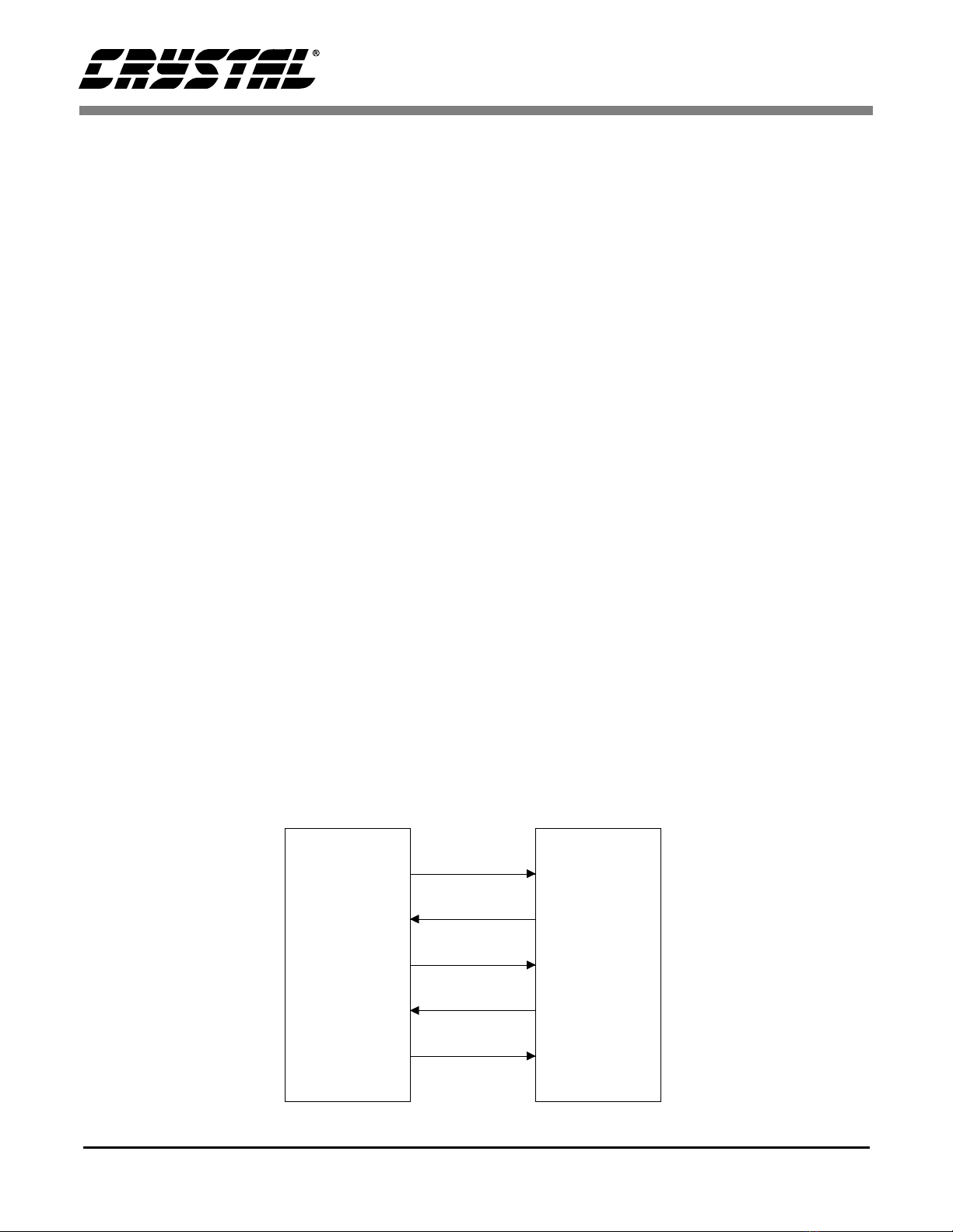
The CS4297A, CS4294, and CS4630 communicate
through a 5-wire serial digital interface known as
the AC-Link, see Figure 1. The AC-Link is used to
transfer digital audio between the devices. It is also
used to send commands from the CS4630 to the au-
dio codec registers. For more information on the
AC-Link, see the AC ’97 specification.
CODEC
SYNC
BIT_CLK
SDATA_OUT
SDATA_IN
RESET#
Digital AC’97
Controller
Figure 1. AC-Link Connections

CRD4630-10
DS445RD10A1 5
2. SCHEMATIC DESCRIPTIONS
This section describes the CRD4630-10 schematic
designs shown in figures 1 through 12. These sche-
matics are also available in the CMK4630-10 man-
ufacturing kit as OrCAD 7.2 files to be used or
modified for individual designs.
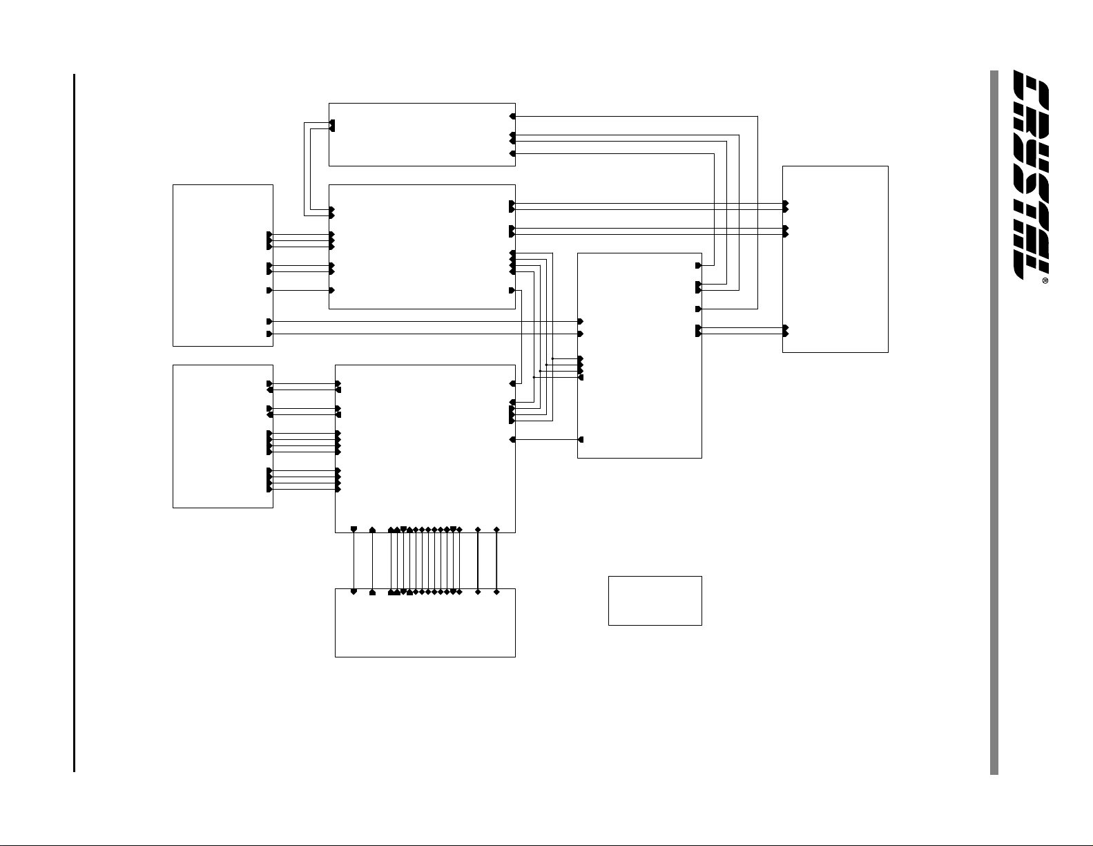
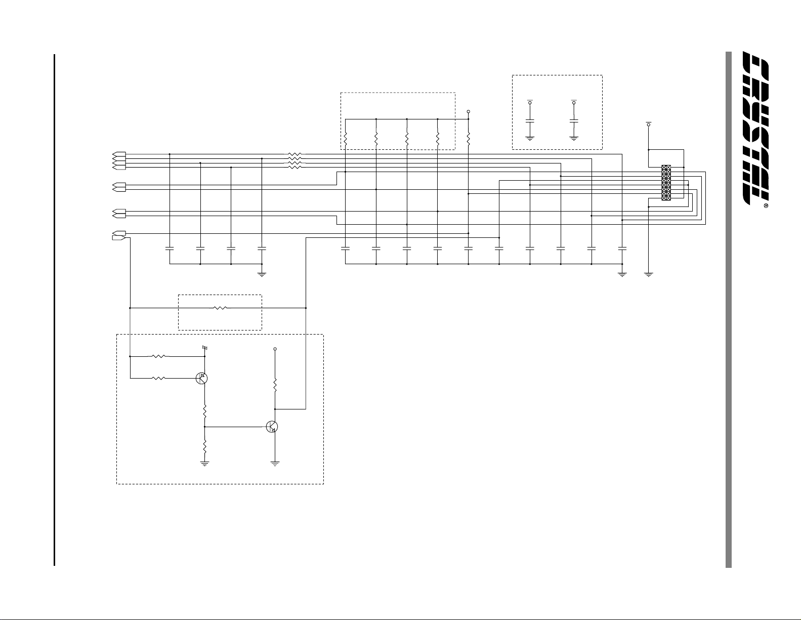
2.1 Block Diagram
The block diagram, shown in Figure 2, illustrates
schematic section interconnection. The schematic
is divided into nine blocks: Analog In, Analog Out,
Line In + Headphone Out, CS4294, CS4297A,
CS4630, Digital I/O, PCI Bus, and Power.
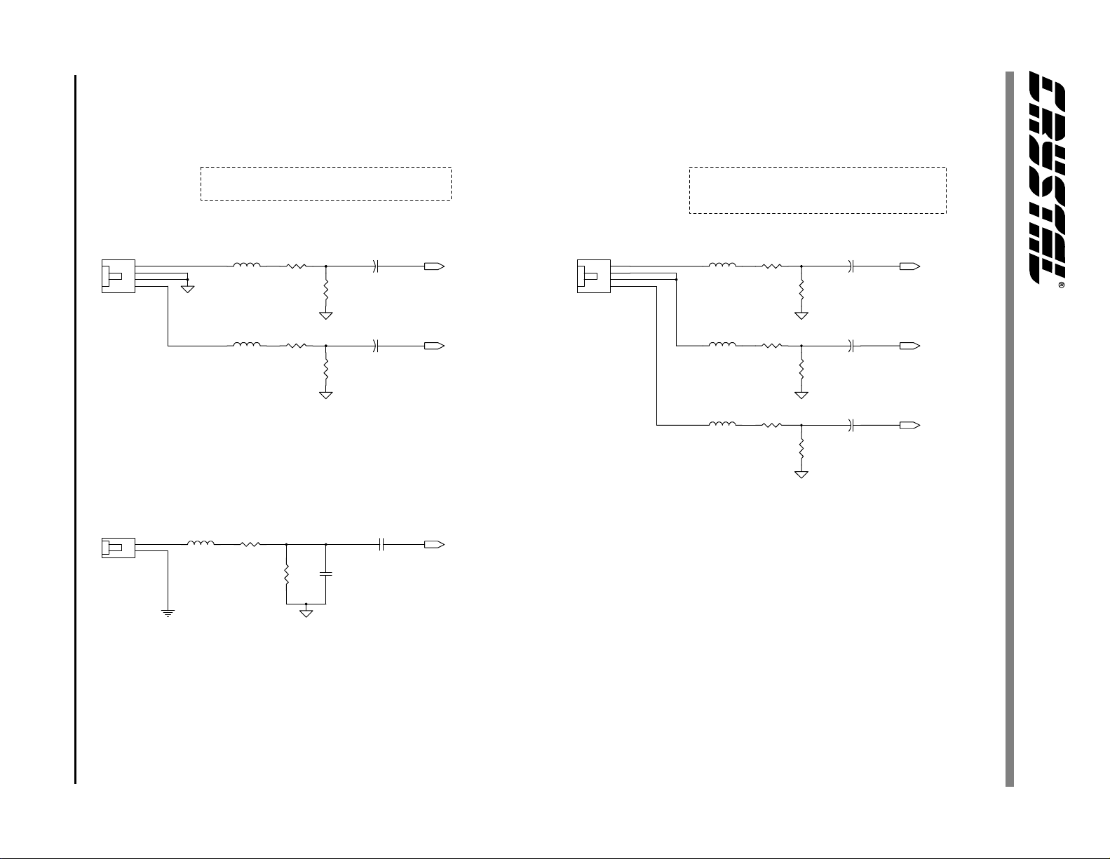
2.2 Analog In
The CRD4630-10 has three stereo (LINE IN,
CD IN, and AUX IN) and two mono (MIC IN and
PC SPEAKER IN) analog inputs. See section 2.4.1
for LINE IN details.
The 220 pF capacitors located on the MIC input,
and the ferrite beads located on the AUX, CD, and
PC_BEEP inputs are provided for EMI suppres-
sion. These components may be removed if EMC
testing determines they are not required.
All analog inputs except PC_BEEP are AC-cou-
pled through a 2.2 µF electrolytic capacitor, mini-
mizing the low frequency roll-off. PC_BEEP is
AC- coupled through a 0.1 µF capacitor.
2.2.1 CD Input
The CD input, shown in Figure 3, ispassed through
a divider circuit that does not reduce the voltage.
This allows for connection of line-level sources up
to 1 Vrms. The divider circuit can be reconfigured
to allow for sources up to 2 Vrms.
The internal CD audio connection, shown in
Figure 3, utilizes a pseudo-differential interface
with CD_COM as the common return path for both
left and right channels. This arrangement reduces
common mode noise picked upalong the CD signal
path.
2.2.2 AUX Input
The AUX input, shown in Figure 3, is passed
through a divider circuit that does not reduce the
voltage. This allows for connection of line-level
sources up to 1 Vrms. The divider circuit can be re-
configured to allow for sources up to 2 Vrms.
2.2.3 Microphone Input
The MIC input pre-amp circuit, shown in Figure 4,
uses a Motorola MC33078D low noise dual op-
amp. One op-amp provides an 18 dB gain stage for
the MIC signal. The other op-amp buffers the phan-
tom power supply. Phantom power is derived from
the +5 V analog supply and buffered by U1A to
provide a maximum of +4.2 V with no load and a
minimum of +2.0 V under a 0.8 mA load, as re-
quired by PC 99. Also included are 3 dB rolloffs at
60 Hz and 15 kHz, as recommended by PC 99.
An alternate, low-cost MIC circuit is also offered.
This circuit maintains the PC 99 requirements for
both MIC phantom power and frequency response,
without providing any boost. The optional primary
audio codec, CS4201, contains up to 30 dB of inter-
nal microphone boost. If replacing the CS4297A
with a CS4201, external boost is not needed.
Both the CS4297A and CS4294 receive the MIC
signal. This allows for several capture options.
2.2.4 PC_BEEP Input
The PC_BEEP input, shown in Figure 3, routes the
PC’s beep tones through the CS4297A. A PC Beep
Bypass feature is used that allows system beep
tones to be heard during a system reset or boot-up.
CRD4630-10
6DS445RD10A1
2.3 Analog Out
The CRD4630-10 has three stereo output signals
providing six channels of audio output
(FRONT OUT, SURROUND OUT, and
CENTER/LFE OUT).
The FRONT, SURROUND, and CENTER/LFE
outputs, shown in Figure 5, provide 1 Vrms line-
level outputs. The 220 pF capacitors provided are
for EMI suppression and may be removed if EMC
testing determines they are not required. Each out-
put is AC-coupled through a 10 µF electrolytic ca-
pacitor, minimizing the low frequency roll-off.
Also provided are 220 kΩbleed-off resistors,
maintaining the audio jacks at 0 V DC.
2.4 Line In + Headphone Out
Audio jack J20, shown in Figure 6, receives either
the LINE input or the HEADPHONE output. Set
jumpers JP2 and JP3 according to the positions list-
ed in Table 1 to determine the functionality of J20.
The 220 pF capacitors provided are for EMI sup-
pression. These components may be removed if
EMC testing determines they are not required.
2.4.1 Line Input
The LINE input, shown in Figure 6, is passed
through a divider circuit reducing the voltage by
6 dB allowing connection of line-level sources up
to 2 Vrms. This input is AC-coupled through
2.2 µF electrolytic capacitors to minimize the low
frequency roll-off.
2.4.2 Headphone Output
The HEADPHONE output circuit, shown in
Figure 6, consists of a Philips TDA1308 low noise
headphone amplifier connected to the
ALT_LINE_OUT signal of the CS4297A. The cir-
cuit has a gain of 3 dB and is capable of driving ste-
reo headphones with impedances of 32 Ωor
greater. The TDA1308 uses a single ended supply
and is biased with Vref from the CS4297A. R119
and R120 are included for short-circuit protection.
An option is provided to bypass the amplifier when
replacing the CS4297A with a CS4201 audio co-
dec. Since the CS4201 contains an integrated head-
phone amplifier, an external headphone amplifier
circuit is not needed.
2.5 CS4294
The CS4294, shown in Figure 7, acts as the second-
ary audio codec for the CRD4630-10. This audio
codec receives the CRD4630-10 AUX, CD, MIC,
and LINE analog inputs. The CS4294 LINE_OUT
and ALT_LINE_OUT signals connect respectively
to the CRD4630-10 SURROUND OUT and CEN-
TER/LFE OUT speaker jacks. All the signals are
AC-coupled.
The primary audio codec, CS4297A, generates the
BIT_CLK AC-Link signal for the CS4294. The
SDATA_IN/ASDIN2 AC-Link signal, created by
the CS4294, is used to communicate with the
CS4630. ASDIN2 has a 47 Ωseries termination re-
sistor to prevent reflections on the AC-Link.
2.6 CS4297A
The CS4297A, shown in Figure 8, acts as the pri-
mary audio codec for the CRD4630-10. This audio
codec receives the CRD4630-10 PC_BEEP and
MIC analog inputs. The CS4297A LINE_OUT and
ALT_LINE_OUT signals connect respectively to
the CRD4630-10 FRONT OUT and HEAD-
PHONE OUT speaker jacks. All the signals are
AC-coupled. Unused analog inputs should be tied
to Vrefout (CS4297A pin 28) or AC-coupled to
ground through a capacitor to prevent noise.
The BIT_CLK and SDATA_IN/ASDIN AC-Link
signals, created by the CS4297A, are used to com-
municate with the CS4630. Both outputs have a
JP2 JP3 Signal Enabled
1-2 1-2 Line Input
2-3 2-3 Headphone Output
Table 1. JP2 and JP3 Position Definitions

CRD4630-10
DS445RD10A1 7
47 Ωseries termination resistor to prevent reflec-
tions on the AC-Link.
An option is provided to replace the CS4297A with
a CS4201 audio codec. In this case, C131 will need
to be changed to a 2.2 µF ceramic capacitor.
2.7 CS4630
The CS4630 audio controller, shown in Figure 9,
acts as a bridge between the PCI bus and the audio
codecs. Communication between the CS4297A,
CS4294, and CS4630 is achieved through the AC-
Link signals. The CS4630 generates three AC-Link
signals, SYNC, SDOUT, and RESET#. The SYNC
and SDOUT outputs have a 47 Ω series termination
resistor to prevent reflections on the AC-Link.
An external EEPROM, U7, is used to provide a
Vendor ID and Subsystem ID to the CS4630 at
power-up. The EEPROM is connected to the
CS4630 through a data and clock signal, EEDAT
and EECLK. The EEPROM interface is enabled by
connecting the EEPDIS pin to digital ground.
The CS4630 requires three power supply voltages:
+3.3 V, +5 V, and +2.5 V. The PCIVDD pins sup-
ply +3.3 V to the CS4630 PCI bus drivers. The
CRYVDD pin supplies +3.3 V to the internal phase
lock loop and crystal oscillator. The VDD5REF pin
is a +5 V pseudo supply for the PCI bus drivers.
This supply enables the PCI interface to support
+5 V signals. The CVDD pins supply +2.5 V to the
core stream processor inside the CS4630. All pow-
er supply pins have a 0.1 µF decoupling capacitor
connected to digital ground.
Unused inputs and bidirectional pins on the
CS4630 are tied to their respective inactive levels
through 220 kΩresistors.
2.8 Digital I/O
The CRD4630-10 digital I/O capabilities include
the Joystick/MIDI interface as well as several
S/PDIF I/O options: S/PDIF opticaloutput, S/PDIF
optical input, and S/PDIF coaxial input.
2.8.1 Joystick/MIDI
The MIDIOUT buffer driver circuit, shown in
Figure 10, provides the +5 V TTL compatible out-
put on J12. If a +3.3 V compatible output is suffi-
cient, remove this circuit and populate R65 to
bypass the buffer circuit. Capacitors C71, C78,
C81, C84, C86, and C89 are provided for EMI sup-
pression and can be removed if EMC testing shows
they are not required. Capacitors C72, C75, C79,
C82, C87, C90, C91 and C95 are functional to the
joystick circuitry, as well as provide for EMI sup-
pression, and must not be removed.
The Joystick/MIDI output on the CRD4630-10 is
not located on the primary bracket, shown in
Figure 18. A short cable is provided to bring the
Joystick/MIDI signal to a secondary bracket,
shown in Figure 19, when using an analog joystick.
If using a USB joystick, the secondary bracket is
not needed.
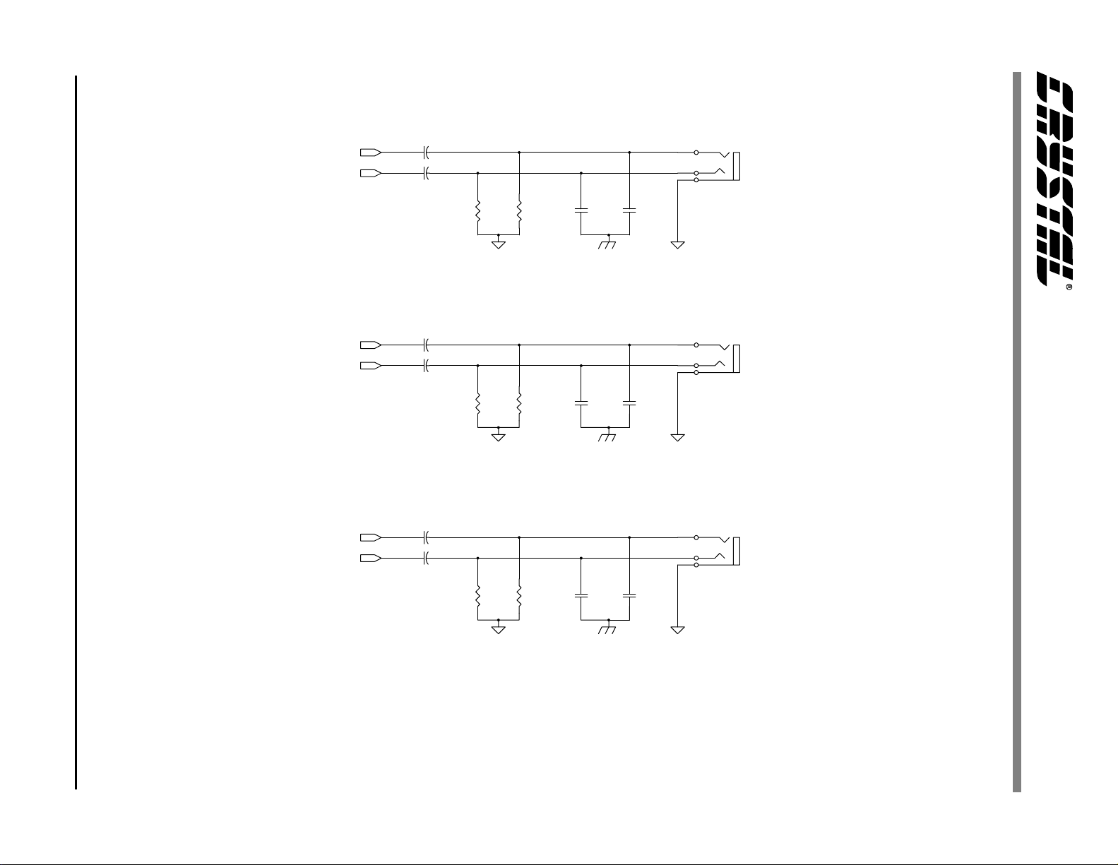
2.8.2 S/PDIF
The S/PDIF (IEC-958) input and output designs,
shown in Figure 11, are compatible with digital in-
puts and outputs on consumer devices such as con-
sumer stereo receivers and MiniDisc recorders.
The CRD4630-10 includes an optical S/PDIF out-
put and two S/PDIF input choices, optical and co-
axial. As shown in Table 2, jumper JP1 controls
which input is enabled.
JP1 Signal Enabled
1-2 S/PDIF In Coaxial
2-3 S/PDIF In Optical
Table 2. JP1 Position Definitions

CRD4630-10
8DS445RD10A1
The S/PDIF output operates at a fixed sampling fre-
quency of 48 kHz. The S/PDIF inputs are capable
of accepting S/PDIF signals with a sample frequen-
cy from 22 kHz up to 48 kHz.
The optical S/PDIF input and output use industry
standard TOSLINK, a digital optical transmitter
and receiver. The input uses a Toshiba TORX-173
digital optical receiver. The output uses a Toshiba
TOTX-173 transmitter.
2.9 PCI Bus
The PCI Local Bus Specification, Revision 2.2 [2]
requires each unused +3.3 V power pin be connect-
ed with an average of 0.01 µF capacitance. Three
0.047 µF capacitors in parallel, shown in
Figure 12, provide the required capacitance. An
option to omit the +3.3 V regulator is offered if this
voltage is known to be provided on the PCI bus.
This is done by populating several 0 Ω resistors:
R84, R85, and R86.
2.10 Power
The CRD4630-10 has three linear voltage regula-
tors, shown in Figure 13, supplying the three re-
quired power supply voltages: +5 V, +3.3 V, and
+2.5 V. The +5 V supply is used exclusively for the
analog audio circuitry surrounding the CS4297A
and CS4294. The +3.3 V supply is used for the au-
dio codecs and controller. The +2.5 V supply, la-
beled +CVDD, is used exclusively for the CS4630.
The +3.3 VD and +CVDD digital power signals are
supplied from the +5 V_PCI signal located on the
PCI bus. A LM1117CST-3.3 regulator supplies
+3.3 VD while a LM2937IMP-2.5 regulator sup-
plies +CVDD. A separate regulator is recommend-
ed for the analog voltage supply to provide good
audio signal quality. A Motorola MC78M05 regu-
lates the +12 VD supply from the PCI bus down to
a clean +5 VA analog supply. For the best audio
performance, the analog voltage regulator should
be located near the audio codecs.
2.11 Component Selection
Great attention was given to the particular compo-
nents used on the CRD4630-10 board with cost,
performance, and package selection as the most im-
portant factors. Listed are some of the guidelines
used in the selection of components:
• No components smaller than 0805 package.
• Single package components; no resistor packs.
• 8-pin devices are in surface mount packages.
2.12 EMI Components
A number of capacitors and inductors are included
to meet EMI compliance tests. These component
values are suggestions only. Actual component val-
ues will depend on your PC board layout and other
design factors. Modify these values as needed in
order to achieve an acceptable EMI profile. Please
refer to Printed Circuit Board Design Techniques
for EMC Compliance [8] for further information on
EMI compliance techniques.

CRD4630-10
DS445RD10A1 9
3. GROUNDING AND LAYOUT
The component layout and signal routing of the
CRD4630-10 provides a good model for laying out
your own PCI add-in card. PCI bus based add-in
cards have explicit requirements on trace lengths
that are not imposed on motherboard designs.
These trace length limits for add-in cards are as fol-
lows:
• Maximum trace length for 32-bit signals on 32-
bit and 64-bit cards is 1.5 inches.
• Maximum trace lengths for signals on the 64-
bit extension are 2 inches.
• Trace length for the PCI CLK signal is
2.5 inches ± 0.1 inch.
• The PCI CLK signal must drive only one load.
Please refer to the PCI Local Bus Specification, Re-
vision 2.2 [2] for information on routing PCI bus
signals on a motherboard.
3.1 Partitioned Voltage and Ground
Planes
The CRD4630-10 is partitioned into separate digi-
tal and analog sections to prevent digital noise from
affecting the performance of the analog circuits.
The analog section is completely isolated from the
digital section, with each section having their own
separate ground plane. All analog components,
power traces and signal traces are routed over the
analog ground plane. Digital components, power
traces and signal traces are not allowed to crossover
into the analog section.
The audio codecs, CS4297A and CS4294, are lo-
cated over the transition point between the analog
and digital ground planes. The pins are arranged on
the audio codecs so that the analog and digital sig-
nals are separated from each other. The analog and
digital ground planes must be tied together for the
codec to maintain proper voltage references. For
best results, the two ground planes are tied together
with a single wide trace between the CS4297A and
the CS4294, near their digital ground pins.
Data converters are generally susceptible to noise
on the crystal pins. In order to reduce coupling
noise on these pins, the area around the crystal and
its signal traces is filled with copper on the top and
bottom of the PCB and attached to digital ground.
A separate chassis ground provides a reference
plane for all the EMI suppression components. The
chassis ground plane is connected to the analog
ground plane at the external jacks.
3.2 CS4297A/CS4294 Layout Notes
Refer to the CS4297A CrystalClearSoundFu-
sionAudio Codec ’97 [4] and the CS4294 Sound-
FusionAudio/Docking Codec ’97 [5] data sheets
for partitioning and bypass capacitor placement.
Pay close attention to bypass capacitors on the
REFFLT, AFLT1, AFLT2 pins, and power supply
capacitors.
CRD4630-10
10 DS445RD10A1
4. REFERENCES
1) Intel®, Audio Codec ’97 Component Specification, Revision 2.1, May 22, 1998.
http://developer.intel.com/ial/scalableplatforms/audio/
2) PCI Special Interest Group, PCI Local Bus Specification, Revision 2.2, December 18, 1998.
http://www.pcisig.com/developers/specification/
3) Cirrus Logic, CS4630 CrystalClearSoundFusionPCI Audio Accelerator Data Sheet
http://www.cirrus.com/pubs/cs4630.pdf
4) Cirrus Logic, CS4297A CrystalClearSoundFusionAudio Codec ’97 Data Sheet
http://www.cirrus.com/pubs/cs4297A.pdf
5) Cirrus Logic, CS4294 SoundFusionAudio/Docking Codec ’97 (AMC’97) Data Sheet
http://www.cirrus.com/pubs/cs4294.pdf
6) Steve Harris, Clif Sanchez, Personal Computer Audio Quality Measurements, Ver 1.0
http://www.cirrus.com/pubs/meas100.pdf
7) Microsoft®, PC 99 System Design Guide, Version 1.0, July 1999,
http://www.microsoft.com/hwdev/desguid/
8) M. Montrose. Printed Circuit Board Design Techniques for EMC Compliance, IEEE Press, New York:
1996.
5. DRAWINGS
• Schematic drawings
• Layout drawings
• Bracket drawings
CRD4630-10
DS445RD10A1 11
POWER
ANALOG IN
MIC_IN_2
CD_IN_R
CD_IN_L
CD_COM
PC_BEEP
AUX_IN_R
AUX_IN_L
MIC_IN_1
LINE IN + HEADPH. OUT
LINE_IN_R
LINE_IN_L
ALT_LINE_OUT_R
ALT_LINE_OUT_L
AVREF
HP_OUT_C
PCI_BUS
PAR
STOP#
TRDY#
FRAME#
INTA#
RST#
GNT#
IDSEL
CLK
REQ#
PERR#
SERR#
IRDY#
DEVSEL#
AD[31..0]
C/BE[3..0]#
DIGITAL I/O
JBCX
JACY
MIDIOUT
JBCY
JACX
JAB2
JBB2
MIDIIN
JAB1
JBB1
SPDIF_RX
SPDIF_TX
CS4630
PERR#
AD[31..0]
JAB1
DEVSEL#
SERR#
CLK
C/BE[3..0]#
PAR
IRDY#
GNT#
JAB2
RST#
ABITCLK
INTA#
JACY
SPDIF_RX
ASDIN
IDSEL
JBB1
FRAME#
MIDIOUT ARST#
STOP#
REQ#
JBCX
ASYNC
TRDY#
JBCY
ASDOUT
SPDIF_TX
MIDIIN
JACX
JBB2
ASDIN2
CS4294
ASDIN2
ASYNC
ARST#
MIC_IN_2
LINE_OUTR_2
ALT_LINE_OUTL_2
ALT_LINE_OUTR_2
LINE_OUTL_2
ASDOUT
ABITCLKAUX_IN_L
AUX_IN_R
CD_IN_L
CD_GND
CD_IN_R
LINE_IN_L
LINE_IN_R
CS4297A
ASYNC
ASDOUT
ASDIN
ARST#
ALT_LINE_OUT_L
ALT_LINE_OUT_R
LINE_OUT_L
LINE_OUT_R
PC_BEEP
MIC_IN_1
ABITCLK
AVREF
HP_OUT_C
ANALOG OUT
LINE_OUT_R_2
LINE_OUT_L_2
ALT_LINE_OUT_L_2
ALT_LINE_OUT_R_2
LINE_OUT_L
LINE_OUT_R
C/BE[3..0]#
AD[31..0]
+12VA ----> +5VA
+5V PCI -----> +3.3VD
+5V PCI -----> +CVDD
Figure 2. CRD4630-10 Block Diagram
CRD4630-10
12 DS445RD10A1
L11
31@100MHz
L14
31@100MHz
L13
31@100MHz
J18
4X1HDR-AU
1
2
3
4
L15
31@100MHz
J19
2X1HDR-SN/PB
1
2
R108
4.7K C148
2700pF
X7R
C147
0.1uF
X7R
J17
4X1HDR-AU
1
2
3
4
L12
31@100MHz
L10
31@100MHz
R107
47K
C144
2.2uF
ELEC
+
C143
2.2uF
ELEC
+
C145
2.2uF
ELEC
+
C146
2.2uF
ELEC
+
R101
100
R98
100
R102
100
R105
100
R103
47K
R100
47K
R104
47K
R106
47K
C142
2.2uF
ELEC
+
R99
47K
R97
100
AGND
AGND
AGND
AGND
AGNDDGND
AGND
AGND
CD_IN_R
CD_IN_L
CD_COM
PC_BEEP
AUX_IN_R
AUX_IN_L
CD IN
PC SPEAKER IN
AUX IN
For 2Vpp CD IN signal:
1) Populate 6.8 kOhms, 1%, for R98, R100, R105 and R106.
2) Populate 3.4 kOhms, 1%, for R102 and R104.
For 2Vpp AUX IN signal:
1) Populate 6.8 kOhms, 1%, for R97, R99, R101 and R103.
Figure 3. Aux, CD, and PC BEEP Inputs

CRD4630-10
DS445RD10A1 13
R17 2.7K
R13
47K
R8
47K
R1 47K
R18
68K
R14 0
C6
0.1uF
X7R R5
0
C4
0.068uF
X7R
J6
PHONO-1/8
4
3
5
2
1
R15
47K
U1A
MC33078D
3
2
1
8 4
+
-
R19
100K
R4
6.8K
1%
C5
0.1uF
Z5U
U1B
MC33078D
5
67
8 4
+
-
C2
10uF
ELEC
+
C15
10uF
ELEC
+
C1 220pF
X7R
C3
220pF
X7R
C12
220pF
X7R
C13
2.2uF
ELEC
+
C11
2.2uF
ELEC
+
AGND
AGND
+5VA
+5VA
+5VA
CGND
AGND
AGND
AGND
AGND
AGND
AGND
+5VA
AGND
MIC_IN_2
MIC_IN_1
Place close to
pins 4 and 8
Connect CGND
to AGND at
the jack
MIC IN
Do not populate
R5 & C6 for
Pre-Amp Mic
Circuit
Do not populate
R14 when using
Pre Amp Mic
Circuit
1) Do not populate U1, R18, R19, R8, R15, R1, R4, C1, C2 and C5.
For Microphone Circuit without Op Amp:
2) Populate R14, R5 and C6
3) Populate:1.5K for R13
100 ohm for C4 (fits on the same pad)
0.22uF for C13
2.2K for R17
Figure 4. Microphone Input
CRD4630-10
14 DS445RD10A1
J15
PHONO-1/8
4
2
1
J16
PHONO-1/8
4
2
1
R89
220K
J14
PHONO-1/8
4
2
1
R90
220K
C112 10uF
ELEC
+
C111 10uF
ELEC
+
C114
220pF
X7R
C113
220pF
X7R
AGND
AGND
AGND CGND AGND
LINE_OUT_R_2
LINE_OUT_L_2
ALT_LINE_OUT_L_2
ALT_LINE_OUT_R_2
LINE_OUT_L
LINE_OUT_R
FRONT
OUT
Connect CGND
to AGND at the
jack.
Connect CGND
to AGND at the
jack.
Connect CGND
to AGND at the
jack.
CENTER/LFE
OUT
C116 10uF
ELEC
+
C115 10uF
ELEC
+
R91
220K R92
220K
AGND
C118
220pF
X7R
C117
220pF
X7R
CGND
SURROUND
OUT
C122
220pF
X7R
C121
220pF
X7R
CGND
R93
220K R94
220K
AGND
C120 10uF
ELEC
+
C119 10uF
ELEC
+
Figure 5. Front, Surround, and Center/LFE Outputs

CRD4630-10
DS445RD10A1 15
JP3
3x1 HDR
1
2
3
R111
6.8K
1%
R110
6.8K
1%
R109
6.8K
1%
J20
PHONO-1/8
4
2
1
JP2
3x1 HDR
1
2
3
C150
220pF
X7R
C152
220pF
X7R
C149
2.2uF
ELEC
C160
1uF
ELEC
+
R116
47K R117
47K
C159
0.1uF
Z5U
C154
220uF
ELEC
+
U15A
TDA1308
3
21
8 4
+
-
C156 22pF
NPO
C155
220uF
ELEC
+
R118
27K
1%
U15B
TDA1308
5
67
8 4
+
-
R115 39K
1%
R114
27K
1%
R120
10
1/4W
R119
10
1/4W
HEADPH_OUT_L
HEADPH_OUT_L
HEADPH_OUT_R
HEADPH_OUT_R
AGND
CGND
AGND
AGND
CGND
AGND
AGND
+5VA
+5VA
+5VA
AGND
AGND
LINE_IN_L
LINE_IN_R
HP_OUT_C
ALT_LINE_OUT_L
AVREF
ALT_LINE_OUT_R
For CS4201 as Primary Codec:
LINE IN/
HEADPHONE
OUT
Connect CGND
to AGND at the
jack.
1. Only populate C160 when CS4201 is primary codec.
2. Place near Headphone Out audio jack.
1) Do not populate U15, C153, C156 and C159.
3) Populate C160 with 1uF ELEC.
Place close
to pins 4
and 8 on
TDA1308
2) Populate R114, R113, R119, R118, R115
and R120 with 0 Ohms.
C151
2.2uF
ELEC
R112
6.8K
1%
C153 22pF
NPO
R113 39K
1%
Figure 6. Line Input and Headphone Output

CRD4630-10
16 DS445RD10A1
R39 47
C46
0.01uF
X7R
C28
1000pF
NPO C50
1000pF
NPO
C23
1000pF
NPO
C25
0.1uF
X7R
C24
0.1uF
X7R
C55
1000pF
NPO
C49
1000pF
NPO
C44
1000pF
NPO
C36
1000pF
NPO
C29
1uF
Y5V
U3
CS4294
LINE_OUT_R 30
AVdd2
31
ALT_LINE_OUT_L 33
ALT_LINE_OUT_R 34
AVss2 32
DVdd1
2
XTL_IN
4XTL_OUT
3
DVss1 5
SDATA_OUT 6
BIT_CLK 7
DVss2 8
SDATA_IN 9
SYNC 11
DVdd2
10
RESET# 12
AUX_L
14 AUX_R
15
CD_L
16 CD_GND
17 CD_R
18 MIC1
19
LINE_IN_L
20 LINE_IN_R
21
AVdd1
22 AVss1 23
REFFLT
24 Vrefout
25
AFLT1
26 AFLT2
27
LINE_OUT_L 29
FLT3D
41 FLTI
42 FLTO
43 GPIO3 1
GPIO4 48
GPIO5 47
GPIO6 46
GPIO7 45
GPIO8 44
ID0# 35
ID1# 28
BCM# 13
AVdd3
36 AVdd4
38 AVss3 37
AVss4 39
AVss5 40
C30
1uF
Y5V
C52
0.1uF
Z5U
C42
0.1uF
Z5U
C31
0.1uF
Z5U
C34
0.1uF
Z5U
C38
0.1uF
Z5U
C41
0.1uF
Z5U
AGND
DGND
+3.3VD +5VA
AGNDAGNDDGND
DGND AGND
+5VA
+3.3VD
AGND
ASDIN2
ASYNC
ARST#
MIC_IN_2 LINE_OUTR_2
ALT_LINE_OUTL_2
ALT_LINE_OUTR_2
LINE_OUTL_2
ASDOUT
ABITCLK
AUX_IN_L
AUX_IN_R
CD_IN_L
CD_GND
CD_IN_R
LINE_IN_L
LINE_IN_R
Figure 7. Secondary Audio Codec, CS4294

CRD4630-10
DS445RD10A1 17
R96 47
Y1
24.576 MHz
C135
1000pF
NPO
C136
1000pF
NPO
C134
0.1uF
X7R
R95 47
C125
1000pF
NPO
U14
CS4297A
LINE_OUT_R 36
MONO_OUT 37
AVdd2
38
ALT_LINE_OUT_L 39
nc7 44
ALT_LINE_OUT_R 41
AVss2 42
nc6 43
nc5 40
FLTO 34
FLTI 33
FLT3D 32
BCFG 31
DVdd1
1
XTL_IN
2XTL_OUT
3
DVss1 4
SDATA_OUT 5
BIT_CLK 6
DVss2 7
SDATA_IN
8SYNC
10
DVdd2
9
RESET#
11
PC_BEEP
12 PHONE
13 AUX_L
14 AUX_R
15 VIDEO_L
16 VIDEO_R
17 CD_L
18 CD_GND
19 CD_R
20 MIC1
21 MIC2
22 LINE_IN_L
23 LINE_IN_R
24
AVdd1
25 AVss1 26
REFFLT
27 Vrefout
28 AFLT1
29 AFLT2
30 S/PDIF_OUT 48
EAPD 47
ID1# 46
ID0# 45
LINE_OUT_L 35
C123
22pF
NPO C124
22pF
NPO
C126
0.01uF
X7R
C127
1000pF
NPO
C128
1000pF
NPO
C129
1000pF
NPO
C130
1000pF
NPO
C132
0.1uF
X7R
C133
1uF
Y5V
C140
0.1uF
Z5U
C141
0.1uF
Z5U
C138
0.1uF
Z5U
C131
1uF
Y5V
C137
0.1uF
Z5U
C139
10uF
ELEC
+
DGND
AGND
DGND
DGND
AGND AGND
+3.3VD
AGND
DGND
+3.3VD +5VA
AGND
AGND
+5VA
ASYNC ASDOUT
ASDIN
ARST#
ALT_LINE_OUT_R
LINE_OUT_L
LINE_OUT_R
PC_BEEP
MIC_IN_1
ABITCLK
AVREF
ALT_LINE_OUT_L
HP_OUT_C
Note: For CS4201 as
primary codec populate
C131 with 2.2uF.
Figure 8. Primary Audio Codec, CS4297A

CRD4630-10
18 DS445RD10A1
R67 47
L7
120 @ 100MHz
R68 47
U7
24LC00
SCL
6
SDA
5
Vcc
8
nc1
1
nc2
2
nc4
7
Vss
4
nc3
3
R73 4.7K
C63
1000pF
NPO
R72
220K
R70
220K
R76
220K
R69 220K
R62 220K
R88
220K R75
220K
C61
0.1uF
Z5U
C69
0.1uF
Z5U
C67
0.1uF
Z5U
C68
0.1uF
Z5U
C99
0.1uF
Z5U
C98
0.1uF
Z5U
C97
0.1uF
Z5U
C93
0.1uF
Z5U
C83
0.1uF
Z5U
C85
0.1uF
Z5U
C80
0.1uF
Z5U
C77
0.1uF
Z5U
C66
0.1uF
Z5U
C92
0.1uF
Z5U
C62
0.1uF
Z5U
U10
CS4630-CM
TEST
65
INTA#
109 RST#
110 PCICLK
111 PCI_GNT#
112 PCI_REQ#
113
CBE[3]# 126
IDSEL
127
CBE[2]# 14
FRAME#
15 IRDY#
24 TRDY
25 DEVSEL#
28 STOP#
31 PERR#
32 SERR#
33 PAR
34
CBE[1]# 35
CBE[0]# 46
AD[31] 116
AD[30] 117
AD[29] 118
AD[28] 119
AD[27] 120
AD[26] 123
AD[24] 125
AD[25] 124
AD[23] 2
AD[22] 3
AD[21] 4
AD[20] 5
AD[19] 6
AD[18] 9
AD[17] 10
AD[16] 11
AD[15] 36
AD[14] 37
AD[12]
41
AD[11]
42
AD[13]
40
AD[10]
43
AD[9]
44
AD[8]
45
AD[7]
49
AD[6]
50
AD[5]
51
AD[4]
52
AD[3]
53
AD[2]
54
AD[1]
55
AD[0]
56
JACX
66
JACY
67
JAB1/SDO2
70 JAB2/SDO3
71
JBCX
68
JBCY
69
JBB1/LRCLK
72 JBB2/MCLK
73
MIDIOUT
77 MIDIIN
74
PCIGND[0] 115
PCIGND[1] 121
PCIGND[2] 1
PCIGND[3] 7
PCIGND[4] 30
PCIGND[5] 38
PCIGND[6] 48
PCIGND[7] 57
CRYVDD 91
CRYGND 94
CGND[0] 26
CGND[1] 13
CGND[2] 76
CGND[3] 79
CGND[4] 89
ABITCLK/SCLK
96
ASDOUT/SDOUT
97
ASDIN/SDIN
98
ASYNC/FSYNC
99 ARST#
100
SDIN2/GPIO/SENSE_VAUX
88 VOLUP/XTALI
92 VOLDN/XTALO
93 EECLK/GPOUT/PCREQ#
101 EEDAT/GPIO2/PCGNT#
102
CVDD[0]
27 CVDD[1]
12
PCIVDD[8]
75
CVDD[2]
78 CVDD[3]
90
PCIVDD[1]
122 PCIVDD[0]
114
PCIVDD[2]
128 PCIVDD[3]
8PCIVDD[4]
29 PCIVDD[5]
39 PCIVDD[6]
47 PCIVDD[7]
58
VDD5REF
95
ARST2#/SELECT_VAUX
62
ASYNC2
61
ASDOUT2
60
ASDIN2
107
ZLRCLK
80 ZSCLK
81 ZSDATA
82
SPDIFI 83
SPDIFO 84
EGPIO[0] 85
EGPIO[1] 86
EGPIO[2] 87
ASCLK/EGPIO[3] 103
104
ASDI/EGPIO[5] 105
ASDO/EGPIO[6] 106
EGPIO[7] 63
CLKRUN# 64
PME#
108
ABITCLK2
59
EEPDIS 23
VAUX_SEL
16
NC2
17 NC3
18 NC4
19 NC5
20
PCIVDD_SENSE
21 VAUX_SENSE
22
AD26
AD25
AD13
AD24
AD20
AD23
AD2
C/BE2
AD7
AD19
AD5
AD18
AD15
AD31
AD3
AD4
AD0
AD17
C/BE3
AD1
C/BE1
C/BE0
AD29
AD28
AD27
AD21
AD16
AD14
AD12
AD11
AD10
AD9
AD8
AD6
AD30
AD22
+3.3VD
+3.3VD
DGND
DGND
DGND DGND
+3.3VD
DGND
+3.3VD
DGND
DGND
DGND
DGND
+3.3VD+3.3VD
DGND
+3.3VD
DGND
DGND
DGND
+3.3VD
DGND
DGND
+5V_PCI
DGND
DGND
DGND
+3.3VD
DGND
DGND
+3.3VD
+CVDD
+CVDD +CVDD +CVDD +CVDD
DGND DGND
DGND
+3.3VD
+3.3VD
DGND
PERR#
AD[31..0]
JAB1
DEVSEL#
SERR#
CLK C/BE[3..0]#
PAR
IRDY#
GNT#
JAB2
RST#
ABITCLK
INTA#
JACY
SPDIF_RX
ASDIN
IDSEL
JBB1
FRAME#
MIDIOUT
ARST#
STOP#
REQ#
JBCX
ASYNC
TRDY#
JBCY
ASDOUT
SPDIF_TX
MIDIIN
JACX
JBB2
ASDIN2
CS4630 AUDIO
ACCELERATOR
CS4630-CM PCIVDD PINS
CS4630-CM CVDD PINS
C100
0.1uF
Z5U
ASFCLK/EGPIO[4]
Figure 9. Audio Controller, CS4630
CRD4630-10
DS445RD10A1 19
C87
5600pF
X7R
C90
5600pF
X7R
C79
5600pF
X7R
C82
5600pF
X7R
R83
4.7K R74
4.7K
R82
4.7K R77
4.7K
C95
1000pF
X7R
C75
1000pF
X7R
C72
1000pF
X7R
R71
47K
C103
0.1uF
Z5U
C64
0.1uF
Z5U
C81
220pF
X7R
C71
220pF
X7R
C78
220pF
X7R
J12 12 34 56 78 910 1112 1314 1516
C84
220pF
X7R
C89
220pF
X7R
C86
220pF
X7R
Q7
MMBT3904LT1
1
3 2
R61
5.1K
R64 39K Q6
MMBT2907ALT1
1
32
R59
10K
R60
20K
R63 39K
R65 100
MIDI_BUF
+5V_JOY+5V_JOY
+5V_PCI
+5V_JOY
DGND DGND
DGND DGND
+3.3VD
DGND
+5V_PCI
DGND
DGND
JBCX
JACY
JBCY
JACX
JAB2
MIDIIN
JAB1
JBB1
MIDIOUT
JBB2
PIN 2
J12 JOYSTICK
SUPPLY PINS
PIN 1
Joystick button pullups still
required on CS462X/CS4280 --
must be populated
optional MIDI out buffer -- populate as necessary
Place Near
CS4630
populate instead of MIDI
out buffer as necessary
2.2K
2.2K
2.2K
2.2K
R79
R81
R80
R78
C91
1000pF
X7R
Figure 10. Joystick/MIDI Interface

CRD4630-10
20 DS445RD10A1
JP1
3x1 HDR
1
2
3
R66 8.2K
R21
1K
L6
47uH
J1
TORX-173
1
2
3
4
5
6
J11
TOTX-173
1
2
3
45
6
U13
SN75179B
R2
D3
A
8B
7
Y
5Z
6
J13
2X1HDR-SN/PB
1
2
C108
0.01uF
X7R C109
0.01uF
X7R
R87
75
C14
0.1uF
Z5U
C110
0.1uF
Z5U
C65
0.1uF
Z5U
+5V_PCI
+5V_PCI
+5V_PCI
+5V_PCI
DGND DGND
DGND
DGND
DGND
DGND
DGND
DGND
DGND
DGND
SPDIF_RX
SPDIF_TX
S/PDIF IN
COAXIAL
Place close
to pins 1
and 4 on
SN75179B
S/PDIF OUT
OPTICAL
S/PDIF IN
OPTICAL
Figure 11. S/PDIF Output and Inputs
Table of contents


