Cypress CYW20734 User manual

CYW20734
Single-Chip Bluetooth Transceiver for
Wireless Input Devices
Cypress Semiconductor Corporation • 198 Champion Court • San Jose,CA 95134-1709 • 408-943-2600
Document Number: 002-14874 Rev. *S Revised Tuesday, October 4, 2016
The Cypress CYW20734 is a Bluetooth 4.1-compliant, stand-alone baseband processor with an integrated 2.4 GHz transceiver.
Manufactured using the industry's most advanced 40 nm CMOS low-power process, the CYW20734 employs the highest level of
integration to eliminate all critical external components, thereby minimizing the device's footprint and the costs associated with
implementing Bluetooth solutions.
The CYW20734 is the optimal solution for applications in wireless input devices including game controllers, remote, keyboards, and
joysticks. Built-in firmware adheres to the Bluetooth Low Energy (BLE) profile and the BLE Human Interface Device (HID) profile.
Cypress Part Numbering Scheme
Cypress is converting the acquired IoT part numbers from Broadcom to the Cypress part numbering scheme. Due to this conversion,
there is no change in form, fit, or function as a result of offering the device with Cypress part number marking. The table provides
Cypress ordering part number that matches an existing IoT part number.
Applications
■Game controllers
■Wireless pointing devices (mice)
■Remote controls
■Wireless keyboards
■Joysticks
■Home automation
■Point-of-sale input devices
■3D glasses
■Blood pressure monitors
■“Find me” devices
■Heart rate monitors
■Proximity sensors
■Thermometers
Features
■Complies with Bluetooth Core Specification version 4.1
including BR/EDR/BLE
■BLE HID profile version 1.00 compliant
■Bluetooth Device ID profile version 1.3 compliant
■Supports Generic Access Profile (GAP)
■Supports Adaptive Frequency Hopping (AFH)
■Excellent receiver sensitivity
■Programmable output power control
■Integrated ARM Cortex-M3 microprocessor core
■On-chip power-on reset (POR)
■Support for EEPROM and serial flash interfaces
■Integrated low dropout regulator (LDO)
■On-chip software controlled power management unit
■Programmable key scan matrix interface, up to 8 × 20 key-
scanning matrix
■Three-axis quadrature signal decoder
■PCM/I2S Interface
■Infrared modulator
■IR learning
■Auxiliary ADC with up to 28 analog channels
■One mono microphone input
■On-chip support for serial peripheral interface (master and
slave modes)
■Broadcom Serial Communications interface (compatible with
NXP I2C slaves)
■Package type:
❐90-pin FBGA package (8.5 mm × 8.5 mm)
❐RoHS compliant
Table 1. Mapping Table for Part Number between Broadcom and Cypress
Broadcom Part Number Cypress Part Number
BCM20734 CYW20734
BCM20734UA1KFFB3G CYW20734UA1KFFB3G

Document Number: 002-14874 Rev. *S Page 2 of 51
CYW20734
Figure 1. Functional Block Diagram
IoT Resources
Cypress provides a wealth of data at http://www.cypress.com/internet-things-iot to help you to select the right IoT device for your
design, and quickly and effectively integrate the device into your design. Cypress provides customer access to a wide range of
information, including technical documentation, schematic diagrams, product bill of materials, PCB layout information, and software
updates. Customers can acquire technical documentation and software from the Cypress Support Community website
(http://community.cypress.com/).
Cortex‐M3 DMA ScanJTAG
Address
Decoder BusArb
Trap&Patch
AHB2APB
WDTimer Remap&
Pause
32‐bitAPB
32‐bitAHB
AHB2MEM
AHB2EBI
External
BusI/F
ROM
AHB2MEM
RAM
PMUControl
UART
Debug
UART
PTU
I/O
PortControl
PMU LPO POR
Buffer
APU
BTClk/
Hopper
BlueRFI/F
Rx/Tx
Buffer
Digital
Modulator
Calibration&
Control
DigitalDemod
BitSync
BluetoothRadio
RF
FlashI/F
JTAG
DigitalI/O
I2C_Master
Interrupt
Controller
PCM
GPIO+Aux SW
Timers JTAGMaster
LCU
SPI
Master
LowPower
Scan
BlueRFRegisters
ADC MIC

Document Number: 002-14874 Rev. *S Page 3 of 51
CYW20734
Contents
1. Functional Description ................................................. 4
1.1 Bluetooth Baseband Core ..................................... 4
1.2 Microprocessor Unit .............................................. 5
1.3 Integrated Radio Transceiver ................................ 6
1.4 Peripheral Transport Unit ...................................... 8
1.5 PCM Interface ..................................................... 10
1.6 Clock Frequencies ...............................................10
1.7 GPIO Ports .......................................................... 12
1.8 Keyboard Scanner ............................................... 12
1.9 Mouse Quadrature Signal Decoder ..................... 13
1.10 ADC Port ...........................................................13
1.11 Microphone Input ............................................... 13
1.12 PWM.................................................................. 14
1.13 Shutter Control for 3D Glasses ......................... 15
1.14 Triac Control ...................................................... 15
1.15 Serial Peripheral Interface ................................. 15
1.16 Infrared Modulator ............................................. 15
1.17 Infrared Learning............................................... 16
1.18 Power Management Unit................................... 16
2. Pin Assignments ........................................................ 17
2.1 Pin Descriptions .................................................. 17
2.2 Ball Map .............................................................. 24
3. Specifications ............................................................. 25
3.1 Electrical Characteristics ..................................... 25
3.2 RF Specifications ................................................ 30
3.3 Timing and AC Characteristics............................ 33
4. Mechanical Information ............................................. 44
4.1 Package Diagram ................................................ 44
4.2 Tape Reel and Packaging Specifications ............ 45
5. Ordering Information .................................................. 46
Document History .......................................................... 48

Document Number: 002-14874 Rev. *S Page 4 of 51
CYW20734
1. Functional Description
1.1 Bluetooth Baseband Core
The Bluetooth Baseband Core (BBC) implements all of the time-critical functions required for high-performance Bluetooth operation.
The BBC manages the buffering, segmentation, and routing of data for all connections. It also buffers data that passes through it,
handles data flow control, schedules SCO/ACL and TX/RX transactions, monitors Bluetooth slot usage, optimally segments and
packages data into baseband packets, manages connection status indicators, and composes and decodes HCI packets. In addition
to these functions, it independently handles HCI event types, and HCI command types.
The following transmit and receive functions are also implemented in the BBC hardware to increase reliability and security of the TX/
RX data before sending over the air:
■Symbol timing recovery, data deframing, forward error correction (FEC), header error control (HEC), cyclic redundancy check
(CRC), data decryption, and data dewhitening in the receiver.
■Data framing, FEC generation, HEC generation, CRC generation, key generation, data encryption, and data whitening in the
transmitter.
1.1.1 Bluetooth 4.0 Features
The BBC supports all Bluetooth 4.0 features, with the following benefits:
■Dual-mode Bluetooth low energy (BT and BLE operation).
■Extended inquiry response (EIR): Shortens the time to retrieve the device name, specific profile, and operating mode.
■Encryption pause resume (EPR): Enables the use of Bluetooth technology in a much more secure environment.
■Sniff subrating (SSR): Optimizes power consumption for low duty cycle asymmetric data flow, which subsequently extends battery
life.
■Secure simple pairing (SSP): Reduces the number of steps for connecting two devices, with minimal or no user interaction required.
■Link supervision time out (LSTO): Additional commands added to HCI and Link Management Protocol (LMP) for improved link
time-out supervision.
■Quality of service (QoS) enhancements: Changes to data traffic control, which results in better link performance. Audio, human
interface device (HID), bulk traffic, SCO, and enhanced SCO (eSCO) are improved with the erroneous data (ED) and packet
boundary flag (PBF) enhancements.
1.1.2 Bluetooth 4.1 Features
The CYW20734 supports the following Bluetooth v4.1 features.
■Secure connections (BR/EDR)
■Fast advertising interval
■Piconet clock adjust
■Connectionless broadcast
■LE privacy v1.1
■Low duty cycle directed advertising
■LE dual mode topology

Document Number: 002-14874 Rev. *S Page 5 of 51
CYW20734
1.1.3 Link Control Layer
The link control layer is part of the Bluetooth link control functions that are implemented in dedicated logic in the link control unit (LCU).
This layer consists of the command controller that takes commands from the software, and other controllers that are activated or
configured by the command controller, to perform the link control tasks. Each task is performed in a different state or substate in the
Bluetooth Link Controller.
■Major states:
❐Standby
❐Connection
■Substates:
❐Page
❐Page Scan
❐Inquiry
❐Inquiry Scan
❐Sniff
1.1.4 Test Mode Support
The CYW20734 fully supports Bluetooth Test mode as described in Part I:1 of the Specification of the Bluetooth System Version 3.0.
This includes the transmitter tests, normal and delayed loopback tests, and reduced hopping sequence.
In addition to the standard Bluetooth Test Mode, the CYW20734 also supports enhanced testing features to simplify RF debugging
and qualification and type-approval testing. These features include:
■Fixed frequency carrier wave (unmodulated) transmission
❐Simplifies some type-approval measurements (Japan)
❐Aids in transmitter performance analysis
■Fixed frequency constant receiver mode
❐Receiver output directed to I/O pin
❐Allows for direct BER measurements using standard RF test equipment
❐Facilitates spurious emissions testing for receive mode
■Fixed frequency constant transmission
❐8-bit fixed pattern or PRBS-9
❐Enables modulated signal measurements with standard RF test equipment
1.1.5 Frequency Hopping Generator
The frequency hopping sequence generator selects the correct hopping channel number based on the link controller state, Bluetooth
clock, and device address.
1.2 Microprocessor Unit
The CYW20734 microprocessor unit runs software from the link control (LC) layer up to the host controller interface (HCI). The
microprocessor is based on the Cortex-M3 32-bit RISC processor with embedded ICE-RT debug and JTAG interface units. The
microprocessor also includes 848 KB of ROM memory for program storage and boot ROM, 352 KB of RAM for data scratch-pad, and
patch RAM code.
The internal boot ROM provides flexibility during power-on reset to enable the same device to be used in various configurations. At
power-up, the lower layer protocol stack is executed from the internal ROM.
External patches can be applied to the ROM-based firmware to provide flexibility for bug fixes and features additions. These patches
can be downloaded using external NVRAM. The device can also support the integration of user applications and profiles using an
external serial flash memory.

Document Number: 002-14874 Rev. *S Page 6 of 51
CYW20734
1.2.1 NVRAM Configuration Data and Storage
NVRAM contains configuration information about the customer application, including the following:
■Fractional-N information
■BD_ADDR
■UART baud rate
■SDP service record
■File system information used for code, code patches, or data. The CYW20734 can use SPI Flash or I2C EEPROMs for NVRAM
storage.
1.2.2 External Reset
An external active-low reset signal, RESET_N, can be used to put the CYW20734 in the reset state. An external voltage detector
reset IC with 50 ms delay is needed on the RESET_N. The RESET_N should be released only after the VDDO supply voltage level
has been stabilized for 50 ms.
Figure 2. Reset Timing
1.3 Integrated Radio Transceiver
The CYW20734 has an integrated radio transceiver that has been optimized for use in 2.4 GHz Bluetooth wireless systems. It has
been designed to provide low-power, low-cost, robust communications for applications operating in the globally available 2.4 GHz
unlicensed ISM band. The CYW20734 is fully compliant with the Bluetooth Radio Specification and enhanced data rate (EDR)
specification and meets or exceeds the requirements to provide the highest communication link quality of service.
VDDIO POR
VDDIO
Reset
(External)
VDDC
50 ms
VDDC Reset (Internal)
XTAL_RESET
XTAL_BUF_PU
~2.4 ms
0.5 ms
~2.4 ms
10 LPO cycles
8 LPO cycles

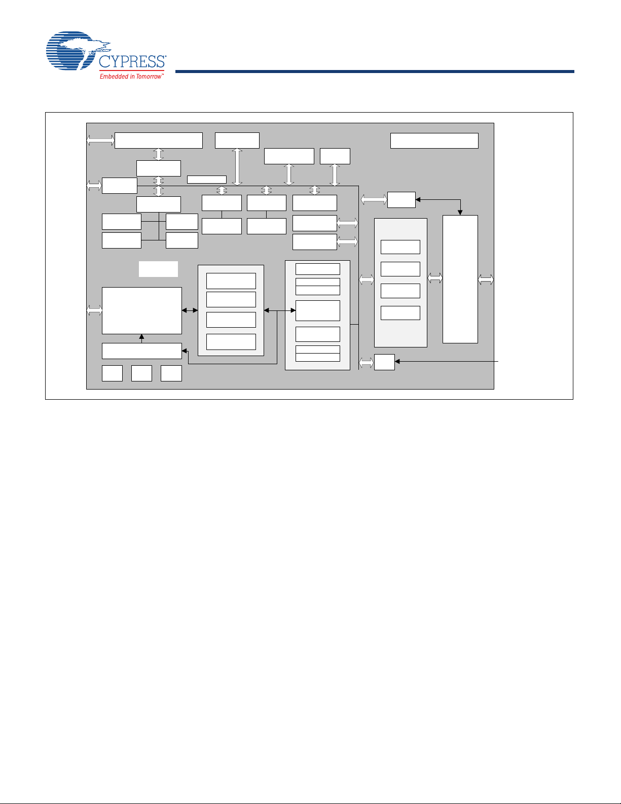
Document Number: 002-14874 Rev. *S Page 7 of 51
CYW20734
1.3.1 Transmit
The CYW20734 features a fully integrated zero-IF transmitter. The baseband transmit data is GFSK-modulated in the modem block
and upconverted to the 2.4 GHz ISM band in the transmitter path. The transmitter path consists of signal filtering, I/Q upconversion,
output power amplifier, and RF filtering. The transmitter path also incorporates /4-DQPSK for 2 Mbps and 8-DPSK for 3 Mbps to
support EDR. The transmitter section is compatible to the Bluetooth Low Energy specification. The transmitter PA bias can also be
adjusted to provide Bluetooth class 1 or class 2 operation.
1.3.2 Digital Modulator
The digital modulator performs the data modulation and filtering required for the GFSK, /4-DQPSK, and
8-DPSK signal. The fully digital modulator minimizes any frequency drift or anomalies in the modulation characteristics of the trans-
mitted signal and is much more stable than direct VCO modulation schemes.
1.3.3 Digital Demodulator and Bit Synchronizer
The digital demodulator and bit synchronizer take the low-IF received signal and perform an optimal frequency tracking and bit-
synchronization algorithm.
1.3.4 Power Amplifier
The fully integrated PA supports Class 1 or Class 2 output using a highly linearized, temperature-compensated design. This provides
greater flexibility in front-end matching and filtering. Due to the linear nature of the PA combined with some integrated filtering, external
filtering is required to meet the Bluetooth and regulatory harmonic and spurious requirements. For integrated mobile handset appli-
cations in which Bluetooth is integrated next to the cellular radio, external filtering can be applied to achieve near thermal noise levels
for spurious and radiated noise emissions. The transmitter features a sophisticated on-chip transmit signal strength indicator (TSSI)
block to keep the absolute output power variation within a tight range across process, voltage, and temperature.
1.3.5 Receiver
The receiver path uses a low-IF scheme to downconvert the received signal for demodulation in the digital demodulator and bit
synchronizer. The receiver path provides a high degree of linearity, an extended dynamic range, and high-order on-chip channel
filtering to ensure reliable operation in the noisy 2.4 GHz ISM band. The front-end topology, with built-in out-of-band attenuation,
enables the CYW20734 to be used in most applications with minimal off-chip filtering. For integrated handset operation, in which the
Bluetooth function is integrated close to the cellular transmitter, external filtering is required to eliminate the desensitization of the
receiver by the cellular transmit signal.
1.3.6 Digital Demodulator and Bit Synchronizer
The digital demodulator and bit synchronizer take the low-IF received signal and perform an optimal frequency tracking and bit
synchronization algorithm.
1.3.7 Receiver Signal Strength Indicator
The radio portion of the CYW20734 provides a receiver signal strength indicator (RSSI) signal to the baseband, so that the controller
can take part in a Bluetooth power-controlled link by providing a metric of its own receiver signal strength to determine whether the
transmitter should increase or decrease its output power.
1.3.8 Local Oscillator Generation
A local oscillator (LO) generation provides fast frequency hopping (1600 hops/second) across the 79 maximum available channels.
The LO generation subblock employs an architecture for high immunity to LO pulling during PA operation. The CYW20734 uses an
internal RF and IF loop filter.
1.3.9 Calibration
The CYW20734 radio transceiver features an automated calibration scheme that is fully self-contained in the radio. No user interaction
is required during normal operation or during manufacturing to provide optimal performance. Calibration tunes the performance of all
the major blocks within the radio to within 2% of optimal conditions, including gain and phase characteristics of filters, matching
between key components, and key gain blocks. This takes into account process variation and temperature variation. Calibration occurs
transparently during normal operation during the settling time of the hops, and calibrates for temperature variations as the device
cools and heats during normal operation in its environment.
1.3.10 Internal LDO
The CYW20734 has a 1.2V internal LDO that supplies power to the baseband and the radio.

Document Number: 002-14874 Rev. *S Page 8 of 51
CYW20734
1.4 Peripheral Transport Unit
1.4.1 Broadcom Serial Communications Interface
The CYW20734 provides a 2-pin master BSC interface, which can be used to retrieve configuration information from an external
EEPROM or to communicate with peripherals such as track-ball or touch-pad modules, and motion tracking ICs used in mouse
devices. The BSC interface is compatible with I2C slave devices. BSC does not support multimaster capability or flexible wait-state
insertion by either master or slave devices.
The following transfer clock rates are supported by BSC:
■100 kHz
■400 kHz
■800 kHz (Not a standard I2C-compatible speed.)
■1 MHz (Compatibility with high-speed I2C-compatible devices is not guaranteed.)
The following transfer types are supported by BSC:
■Read (Up to 127 bytes can be read.)
■Write (Up to 127 bytes can be written.)
■Read-then-Write (Up to 127 bytes can be read and up to 127 bytes can be written.)
■Write-then-Read (Up to 127 bytes can be written and up to 127 bytes can be read.)
Hardware controls the transfers, requiring minimal firmware setup and supervision.
The clock pin (SCL) and data pin (SDA) are both open-drain I/O pins. Pull-up resistors external to the CYW20734 are required on
both the SCL and SDA pins for proper operation.
1.4.2 UART Interface
The UART physical interface is a standard, 4-wire interface (RX, TX, RTS, and CTS) with adjustable baud rates from 9600 bps to 6
Mbps. During initial boot, UART speeds may be limited to 750 kbps. The baud rate may be selected via a vendor-specific UART HCI
command. The CYW20734 has a 1040-byte receive FIFO and a 1040-byte transmit FIFO to support enhanced data rates. The
interface supports the Bluetooth UART HCI (H4) specification. The default baud rate for H4 is 115.2 kbaud.
The UART clock default setting is 24 MHz, and can be configured to run as high as 48 MHz to support up to 6 Mbps. The baud rate
of the CYW20734 UART is controlled by two values. The first is a UART clock divisor (set in the DLBR register) that divides the UART
clock by an integer multiple of 16. The second is a baud rate adjustment (set in the DHBR register) that is used to specify a number
of UART clock cycles to stuff in the first or second half of each bit time. Up to eight UART cycles can be inserted into the first half of
each bit time, and up to eight UART clock cycles can be inserted into the end of each bit time.
Tabl e 2 contains example values to generate common baud rates with a 24 MHz UART clock.
Table 2. Common Baud Rate Examples, 24 MHz Clock
Baud Rate (bps) Baud Rate Adjustment Mode Error (%)
High Nibble Low Nibble
3M 0xFF 0xF8 High rate 0.00
2M 0XFF 0XF4 High rate 0.00
1M 0X44 0XFF Normal 0.00
921600 0x05 0x05 Normal 0.16
460800 0x02 0x02 Normal 0.16
230400 0x04 0x04 Normal 0.16
115200 0x00 0x00 Normal 0.16
57600 0x00 0x00 Normal 0.16
38400 0x01 0x00 Normal 0.00
28800 0x00 0x00 Normal 0.16
19200 0x01 0x01 Normal 0.00
14400 0x00 0x00 Normal 0.16
9600 0x02 0x02 Normal 0.00

Document Number: 002-14874 Rev. *S Page 9 of 51
CYW20734
Tabl e 3 contains example values to generate common baud rates with a 48 MHz UART clock.
Normally, the UART baud rate is set by a configuration record downloaded after reset. Support for changing the baud rate during
normal HCI UART operation is included through a vendor-specific command that allows the host to adjust the contents of the baud
rate registers.
The CYW20734 UART operates correctly with the host UART as long as the combined baud rate error of the two devices is within
±2.5%. This should include all temperature, voltage, and process variation dependent offsets.
1.4.3 Peripheral UART Interface
The CYW20734 has a second UART that may be used to interface to other peripherals. This peripheral UART is accessed through
the optional I/O ports, which can be configured individually and separately for each functional pin as shown in Table 4.
Table 3. Common Baud Rate Examples, 48 MHz Clock
Baud Rate (bps) High Rate Low Rate Mode Error (%)
6M 0xFF 0xF8 High rate 0
4M 0xFF 0xF4 High rate 0
3M 0x0 0xFF Normal 0
2M 0x44 0xFF Normal 0
1.5M 0x0 0xFE Normal 0
1M 0x0 0xFD Normal 0
921600 0x22 0xFD Normal 0.16
230400 0x0 0xF3 Normal 0.16
115200 0x1 0xE6 Normal –0.08
57600 0x1 0xCC Normal 0.04
38400 0x11 0xB2 Normal 0
19200 0x22 0x64 Normal 0
Table 4. CYW20734 Peripheral UART
Pin Name pUART_TX pUART_RX pUART_CTS_N pUART_RTS_N
Configured pin name P0 P2 P3 P1
P5 P4 P7 P6
P24 P25 P35 P30
P31 P33 – –
P32 P34 – –

Document Number: 002-14874 Rev. *S Page 10 of 51
CYW20734
1.5 PCM Interface
The CYW20734 includes a PCM interface that shares pins with the I2S interface. The PCM Interface on the CYW20734 can connect
to linear PCM codec devices in master or slave mode. In master mode, the CYW20734 generates the PCM_CLK and PCM_SYNC
signals. In slave mode, these signals are provided by another master on the PCM interface and are inputs to the CYW20734.
The configuration of the PCM interface may be adjusted by the host through the use of vendor-specific HCI commands.
1.5.1 Slot Mapping
The CYW20734 supports up to three simultaneous full-duplex SCO or eSCO channels through the PCM interface. These three
channels are time-multiplexed onto the single PCM interface by using a time-slotting scheme where the 8 kHz or 16 kHz audio sample
interval is divided into as many as 16 slots. The number of slots is dependent on the selected interface rate (128 kHz, 512 kHz, or
1024 kHz). The corresponding number of slots for these interface rate is 1, 2, 4, 8, and 16, respectively. Transmit and receive PCM
data from an SCO channel is always mapped to the same slot. The PCM data output driver tristates its output on unused slots to allow
other devices to share the same PCM interface signals. The data output driver tristates its output after the falling edge of the PCM
clock during the last bit of the slot.
1.5.2 Frame Synchronization
The CYW20734 supports both short- and long-frame synchronization in both master and slave modes. In short-frame synchronization
mode, the frame synchronization signal is an active-high pulse at the audio frame rate that is a single-bit period in width and is
synchronized to the rising edge of the bit clock. The PCM slave looks for a high on the falling edge of the bit clock and expects the
first bit of the first slot to start at the next rising edge of the clock. In long-frame synchronization mode, the frame synchronization
signal is again an active-high pulse at the audio frame rate; however, the duration is three bit periods and the pulse starts coincident
with the first bit of the first slot.
1.5.3 Data Formatting
The CYW20734 may be configured to generate and accept several different data formats. For conventional narrowband speech mode,
the CYW20734 uses 13 of the 16 bits in each PCM frame. The location and order of these 13 bits can be configured to support various
data formats on the PCM interface. The remaining three bits are ignored on the input and may be filled with 0s, 1s, a sign bit, or a
programmed value on the output. The default format is 13-bit 2’s complement data, left justified, and clocked MSB first.
1.5.4 Burst PCM Mode
In this mode of operation, the PCM bus runs at a significantly higher rate of operation to allow the host to duty cycle its operation and
save current. In this mode of operation, the PCM bus can operate at a rate of up to 24 MHz. This mode of operation is initiated with
an HCI command from the host.
1.6 Clock Frequencies
The CYW20734 uses a 24 MHz crystal oscillator (XTAL).
1.6.1 Crystal Oscillator
The XTAL must have an accuracy of ±20 ppm as defined by the Bluetooth specification. Two external load capacitors in the range of
5 pF to 30 pF are required to work with the crystal oscillator. The selection of the load capacitors is XTAL-dependent (see Figure 3).
Figure 3. Recommended Oscillator Configuration—12 pF Load Crystal
22pF
20pF
Crystal
XIN
XOUT

Document Number: 002-14874 Rev. *S Page 11 of 51
CYW20734
Tabl e 5showstherecommendedcrystalspecifications.
1.6.2 HID Peripheral Block
The peripheral blocks of the CYW20734 all run from a single 128 kHz low-power RC oscillator. The oscillator can be turned on at the
request of any of the peripherals. If the peripheral is not enabled, it shall not assert its clock request line.
The keyboard scanner is a special case, in that it may drop its clock request line even when enabled, and then reassert the clock
request line if a keypress is detected.
1.6.3 32 kHz Crystal Oscillator
Figure 4 shows the 32 kHz XTAL oscillator with external components and Table 6 lists the oscillator’s characteristics. It is a standard
Pierce oscillator using a comparator with hysteresis on the output to create a single-ended digital output. The hysteresis was added
to eliminate any chatter when the input is around the threshold of the comparator and is ~100 mV. This circuit can be operated with
a 32 kHz or 32.768 kHz crystal oscillator or be driven with a clock input at similar frequency. The default component values are: R1
= 10 MΩand C1 = C2 = ~10 pF. The values of C1 and C2 are used to fine-tune the oscillator.
Figure 4. 32 kHz Oscillator Block Diagram
Table 5. Reference Crystal Electrical Specifications
Parameter Conditions Minimum Typical Maximum Unit
Nominal frequency – – 24.000 – MHz
Oscillation mode – Fundamental –
Frequency tolerance @25°C – ±10 – ppm
Tolerance stability over temp @0°C to +70°C – ±10 – ppm
Equivalent series resistance – – – 50
Load capacitance – – 12 – pF
Operating temperature range – 0 – +70 °C
Storage temperature range – –40 – +125 °C
Drive level – – – 200 μW
Aging – – – ±10 ppm/year
Shunt capacitance – – – 2 pF
C2
C1
R1 32.768kHz
XTAL

Document Number: 002-14874 Rev. *S Page 12 of 51
CYW20734
1.7 GPIO Ports
The CYW20734 has 40 general-purpose I/Os (GPIOs) in a 90-pin package. All GPIOs support programmable pull-ups and are capable
of driving up to 8 mA at 3.3V or 4 mA at 1.8V, except P26, P27, P28, and P29, which are capable of driving up to 16 mA at 3.3V or
8 mA at 1.8V.
Port 0–Port 1, Port 8–Port 19, Port 21–Port 23, and Port 28–Port 38
All of these pins can be programmed as ADC inputs.
Port 26–Port 29
P[26:29] consist of four pins. All pins are capable of sinking up to 16 mA for LEDs. These pins also have the PWM function, which
can be used for LED dimming.
1.8 Keyboard Scanner
The keyboard scanner is designed to autonomously sample keys and store them into buffer registers without the need for the host
microcontroller to intervene. The scanner has the following features:
■Ability to turn off its clock if no keys are pressed.
■Sequential scanning of up to 160 keys in an 8 × 20 matrix.
■Programmable number of columns from 1 to 20.
■Programmable number of rows from 1 to 8.
■16-byte key-code buffer (can be augmented by firmware).
■128 kHz clock that allows scanning of full 160-key matrix in about 1.2 ms.
■N-key rollover with selective 2-key lockout if ghost is detected.
■Keys are buffered until host microcontroller has a chance to read it, or until overflow occurs.
■Hardware debouncing and noise/glitch filtering.
■Low-power consumption. Single-digit µA-level sleep current.
1.8.1 Theory of Operation
The key scan block is controlled by a state machine with the following states:
1.8.2 Idle
The state machine begins in the idle state. In this state, all column outputs are driven high. If any key is pressed, a transition occurs
on one of the row inputs. This transition causes the 128 kHz clock to be enabled (if it is not already enabled by another peripheral)
and the state machine to enter the scan state. Also in this state, an
8-bit row-hit register and an 8-bit key-index counter is reset to 0.
Table 6. XTAL Oscillator Characteristics
Parameter Symbol Conditions Minimum Typical Maximum Unit
Output frequency Foscout – – 32.768 – kHz
Frequency tolerance – Crystal-dependent – 100 – ppm
Start-up time Tstartup –––500ms
XTAL drive level Pdrv For crystal selection 0.5 – – μW
XTAL series resistance Rseries For crystal selection – – 70 kΩ
XTAL shunt capacitance Cshunt For crystal selection – – 1.3 pF

Document Number: 002-14874 Rev. *S Page 13 of 51
CYW20734
1.8.3 Scan
In the scan state, a row counter counts from 0 up to a programmable number of rows minus 1. After the last row is reached, the row
counter is reset and the column counter is incremented. This cycle repeats until the row and column counters are both at their
respective terminal count values. At that point, the state machine moves into the Scan-End state.
As the keys are being scanned, the key-index counter is incremented. This counter value is compared to the modifier key codes stored
in RAM, or in the key-code buffer if the key is not a modifier key. It can be used by the microprocessor as an index into a lookup table
of usage codes.
Also, as the nth row is scanned, the row-hit register is ORed with the current 8-bit row input values if the current column contains two
or more row hits. During the scan of any column, if a key is detected at the current row, and the row-hit register indicates that a hit
was detected in that same row on a previous column, then a ghost condition may have occurred, and a bit in the status register is set
to indicate this.
1.8.4 Scan End
This state determines whether any keys were detected while in the scan state. If yes, the state machine returns to the scan state. If
no, the state machine returns to the idle state, and the 128 kHz clock request signal is made inactive.
Note: The microcontroller can poll the key status register.
1.9 Mouse Quadrature Signal Decoder
The mouse signal decoder is designed to autonomously sample two quadrature signals commonly generated by an optomechanical
mouse. The decoder has the following features:
■Three pairs of inputs for X, Y, and Z (typical scroll wheel) axis signals. Each axis has two options:
❐For the X axis, choose P2 or P32 as X0 and P3 or P33 as X1.
❐For the Y axis, choose P4 or P34 as Y0 and P5 or P35 as Y1.
❐For the Z axis, choose P6 or P36 as Z0 and P7 or P37 as Z1.
■Control of up to four external high-current GPIOs to power external optoelectronics:
❐Turn-on and turn-off time can be staggered for each HC-GPIO to avoid simultaneous switching of high currents and having multiple
high-current devices on at the same time.
❐Sample time can be staggered for each axis.
❐Sense of the control signal can be active high or active low.
❐Control signal can be tristated for off condition or driven high or low, as appropriate.
1.9.1 Theory of Operation
The mouse decoder block has four 10-bit PWMs for controlling external quadrature devices and sampling the quadrature inputs at its
core.
The GPIO signals may be used to control such items as LEDs, external ICs that may emulate quadrature signals, photodiodes, and
photodetectors.
1.10 ADC Port
The ADC block is a single switched-cap Σ-∆ADC core for audio and DC measurement. It operates at the 12 MHz clock rate and has
32 DC input channels, including 28 GPIO inputs. The internal bandgap reference has ±5% accuracy without calibration. Different
calibration and digital correction schemes can be applied to reduce ADC absolute error and improve measurement accuracy in DC
mode.
1.11 Microphone Input
The CYW20734 integrates support for a differential or single-ended mono microphone. This reduces the requirement on external
components because there is no need for a separate microphone amplifier. The microphone input has a user-programmable gain
range of 0–42 dB with 3 dB steps. A microphone bias output from the chip is provided that can be used to bias an electret condenser-
type microphone. The MIC Bias reference output voltage is 2.1V or 21/25 of the audio power supply. The MIC block can be powered
down when it is not in use.

Document Number: 002-14874 Rev. *S Page 14 of 51
CYW20734
1.12 PWM
The CYW20734 has four internal PWMs. The PWM module consists of the following:
■PWM1–4
■Each of the four PWM channels, PWM1–4, contains the following registers:
❐10-bit initial value register (read/write)
❐10-bit toggle register (read/write)
❐10-bit PWM counter value register (read)
■PWM configuration register shared among PWM1–4 (read/write). This 12-bit register is used:
❐To configure each PWM channel
❐To select the clock of each PWM channel
❐To change the phase of each PWM channel
Figure 5 shows the structure of one PWM.
Figure 5. PWM Block Diagram
pwm_cfg_adrregister pwm#_init_val_adrregister pwm#_togg_val_adrregister
pwm#_cntr_adr
enable
cntrvalueisARMreadable
clk_sel
o_flip
10'H000
10'H3FF
10
10 10
Example:PWMcntrw/pwm#_init_val=0(dashedline)
PWMcntrw/pwm#_init_val=x(solidline)
10'Hx
pwm_out
pwm_togg_val_adr
pwm_out

Document Number: 002-14874 Rev. *S Page 15 of 51
CYW20734
1.13 Shutter Control for 3D Glasses
The CYW20734, combined with the Cypress Bluetooth host device, provides full system support for 3D glasses on televisions. The
Cypress Bluetooth host device gets frame synchronization signals from the TV, converts them into proprietary timing control
messages, then passes the messages to the CYW20734. The CYW20734 uses these messages to synchronize the shutter control
for the 3D glasses with the television frames.
The CYW20734 can provide up to four synchronized control signals for left and right eye shutter control. These four lines can output
pulses with microsecond resolution for on and off timing. The total cycle time can be set for any period up to 65535 msec. The pulses
are synchronized to each other for left and right eye shutters.
The CYW20734 seamlessly adjusts the timing of the control signals based on control messages from the Cypress Bluetooth host
device, ensuring that the 3D glasses remain synchronized to the TV display frame.
3D hardware control on the CYW20734 works independently of the rest of the system. The CYW20734 negotiates sniff with the
Cypress Bluetooth host device and, except for sniff resynchronization periods, most of the CYW20734 circuitry remains in a low power
state while the 3D glasses subsystem continues to provide shutter timing and control pulses. This significantly reduces total system
power consumption.
1.14 Triac Control
The CYW20734 includes hardware support for zero-crossing detection and trigger control for up to four triacs. The CYW20734 detects
zero-crossing on the AC zero detection line and uses that to provide a pulse that is offset from the zero crossing. This allows the
CYW20734 to be used in dimmer applications, as well as any other applications that require a control signal that is offset from an
input event.
The zero-crossing hardware includes an option to suppress glitches.
1.15 Serial Peripheral Interface
The CYW20734 has two independent SPI interfaces. One is a master-only interface (SPI_2) and the other (SPI_1) can be either a
master or a slave. Each interface has a 64-byte transmit buffer and a 64-byte receive buffer. To support more flexibility for user
applications, the CYW20734 has optional I/O ports that can be configured individually and separately for each functional pin. The
CYW20734 acts as an SPI master device that supports 1.8V or 3.3V SPI slaves. The CYW20734 can also act as an SPI slave device
that supports a 1.8V or 3.3V SPI master.
Note: SPI voltage depends on VDDO/VDDM; therefore, it defines the type of devices that can be supported.
1.16 Infrared Modulator
The CYW20734 includes hardware support for infrared TX. The hardware can transmit both modulated and unmodulated waveforms.
For modulated waveforms, hardware inserts the desired carrier frequency into all IR transmissions. IR TX can be sourced from
firmware-supplied descriptors, a programmable bit, or the peripheral UART transmitter.
If descriptors are used, they include IR on/off state and the duration between 1–32767 µsec. The CYW20734 IR TX firmware driver
inserts this information in a hardware FIFO and makes sure that all descriptors are played out without a glitch due to underrun (see
Figure 6).
Figure 6. Infrared TX

Document Number: 002-14874 Rev. *S Page 16 of 51
CYW20734
1.17 Infrared Learning
The CYW20734 includes hardware support for infrared learning. The hardware can detect both modulated and unmodulated signals.
For modulated signals, the CYW20734 can detect carrier frequencies between 10 kHz and 500 kHz, and the duration that the signal
is present or absent. The CYW20734 firmware driver supports further analysis and compression of the learned signal. The learned
signal can then be played back through the CYW20734 IR TX subsystem (see Figure 7).
Figure 7. Infrared RX
1.18 Power Management Unit
The Power Management Unit (PMU) provides power management features that can be invoked by software through power
management registers or packet-handling in the baseband core.
1.18.1 RF Power Management
The BBC generates power-down control signals for the transmit path, receive path, PLL, and power amplifier to the 2.4 GHz trans-
ceiver, which then processes the power-down functions accordingly.
1.18.2 Host Controller Power Management
Power is automatically managed by the firmware based on input device activity. As a power-saving task, the firmware controls the
disabling of the on-chip regulator when in HIDOFF (deep sleep) mode.
1.18.3 BBC Power Management
There are several low-power operations for the BBC:
■Physical layer packet handling turns RF on and off dynamically within packet TX and RX.
■Bluetooth-specified low-power connection mode. While in these low-power connection modes, the CYW20734 runs on the Low
Power Oscillator and wakes up after a predefined time period.
The CYW20734 automatically adjusts its power dissipation based on user activity. The following power modes are supported:
■Active mode
■Idle mode
■Sleep mode
■HIDOFF (deep sleep) mode
The CYW20734 transitions to the next lower state after a programmable period of user inactivity. When user activity resumes, the
CYW20734 immediately enters Active mode.
In HIDOFF mode, the CYW20734 baseband and core are powered off by disabling power to VDDC_OUT and PAVDD. The VDDO
domain remains powered up and will turn the remainder of the chip on when it detects user events. This mode minimizes chip power
consumption and is intended for long periods of inactivity.

Document Number: 002-14874 Rev. *S Page 17 of 51
CYW20734
2. Pin Assignments
2.1 Pin Descriptions
Table 7. Pin Descriptions
Pin Number Pin Name I/O Power Domain Description
Radio I/O
A1 RFOP I/O PAVDD RF antenna port
RF Power Supplies
D1 IFVDD1P2 I IFVDD1P2 IFPLL power supply
B1 LNAVDD1P2 I LNAVDD1P2 RF front-end supply
C1 VCOVDD1P2 I VCOVDD1P2 VCO supply
B2 PLLVDD1P2 I PLLVDD1P2 RFPLL and crystal oscillator supply
A3 PAVDD O PAVDD PA supply
Power Supplies
F1, G3 VDDC I VDDC Baseband core supply
A9, K1 VDDO I VDDO I/O pad and core supply
B6 MIC_AVDD I MIC_AVDD Microphone supply
A5 ADC_AVBAT I ADC_AVBAT ADC supply
A8 ADC_AVDDC I ADC_AVDDC ADC supply
Ground
A2, A10, B5, C2,
C3, D3, F2, J1, K10
VSS I VSS Ground
B8 AVSS I AVSS Analog ground
Clock Generator and Crystal Interface
B4 XTALI I PLLVDD1P2 Crystal oscillator input. See “Crystal Oscillator” on page 10
for options.
A4 XTALO O PLLVDD1P2 Crystal oscillator output.
E6 XTALI32K I PLLVDD1P2 Low-power oscillator input.
F6 XTALO32K O PLLVDD1P2 Low-power oscillator output.
Core
H3 RESET_N I/O PU VDDO Active-low system reset with open-drain output and internal
pull-up resistor.
F5 TM1 I VDDO Device test mode control.
Connect to GND for all applications.
E5 JTAG_SEL I VDDO ARM JTAG debug mode control.
Connect to GND for all applications.
Microphone
A7 MICP I MIC_AVDD Microphone positive input
B7 MICN I MIC_AVDD Microphone negative input
A6 MIC_BIAS O MIC_AVDD Microphone bias supply
PCM2/I2S
J3 PCM_SYNC I/O, PD VDDO Frame synchronization for PCM interface.
Alternate function:
I2S word select
K2 PCM_CLK I/O, PD VDDO Clock for PCM interface.
Alternate function:
I2S clock

Document Number: 002-14874 Rev. *S Page 18 of 51
CYW20734
K3 PCM_IN I, PU VDDO Data input for PCM interface.
Alternate function:
I2S data input
SDA
J2 PCM_OUT O, PD VDDO Data output for PCM interface.
Alternate function:
I2S data output
SCL
UART
H5 UART_RXD I VDDO UART serial input – Serial data input for the HCI UART
interface.
H4 UART_TXD O, PU VDDO UART serial output – Serial data output for the HCI UART
interface.
J4 UART_RTS_N O, PU VDDO Request to send (RTS) for HCI UART interface. Leave
unconnected if not used.
J5 UART_CTS_N I, PU VDDO Clear to send (CTS) for HCI UART interface. Leave uncon-
nected if not used.
BSC/SPI
H1 SPI_MISO_SCL I/O VDDO BSC clock
G1 SPI_MOSI_SDA I/O VDDO BSC data
G2 SPI_CLK I/O VDDO Serial flash SPI clock
H2 SPI_CSN I/O VDDO Serial flash active-low chip select
LDO Regulator Power Supplies
B3 VBAT I VBAT 1.2V LDO input
E1 VDDC_OUT O VDDC_OUT 1.2V LDO output
Reserved
F4 Reserved0 I VDDO Reserved. Leave unconnected.
D5 Reserved1 I VDDO Reserved. Leave unconnected.
E3 Reserved2 I VDDO Reserved. Connect to GND.
E4 Reserved3 I VDDO Reserved. Leave unconnected.
D4 Reserved4 I VDDO Reserved. Connect to GND.
Table 7. Pin Descriptions (Cont.)
Pin Number Pin Name I/O Power Domain Description

Document Number: 002-14874 Rev. *S Page 19 of 51
CYW20734
Table 8. GPIO Pin Descriptionsa
Pin
Number
Pin
Name
Default Di-
rection
POR
State
Post-Reset
StatebPower Do-
main Alternate Function Description
G7 P0 Input Floating Floating VDDO ■GPIO: P0
■Keyboard scan input (row): KSI0
■A/D converter input 29
■Peripheral UART: puart_tx
■SPI_1: MOSI (master and slave)
■IR_RX
■60Hz_main
Note: Not available during TM1 = 1.
G6 P1 Input Floating Floating VDDO ■GPIO: P1
■Keyboard scan input (row): KSI1
■A/D converter input 28
■Peripheral UART: puart_rts
■SPI_1: MISO (master and slave)
■IR_TX
C9 P2 Input Floating Floating VDDO ■GPIO: P2
■Keyboard scan input (row): KSI2
■Quadrature: QDX0
■Peripheral UART: puart_rx
■SPI_1: SPI_CS (slave only)
■SPI_1: MOSI (master only)
E9 P3 Input Floating Floating VDDO ■GPIO: P3
■Keyboard scan input (row): KSI3
■Quadrature: QDX1
■Peripheral UART: puart_cts
■SPI_1: SPI_CLK (master and slave)
G10 P4 Input Floating Floating VDDO ■GPIO: P4
■Keyboard scan input (row): KSI4
■Quadrature: QDY0
■Peripheral UART: puart_rx
■SPI_1: MOSI (master and slave)
■IR_TX
K4 P5 Input Floating Floating VDDO ■GPIO: P5
■Keyboard scan input (row): KSI5
■Quadrature: QDY1
■Peripheral UART: puart_tx
■SPI_1: MISO (master and slave)
■BSC: SDA

Document Number: 002-14874 Rev. *S Page 20 of 51
CYW20734
G4 P6 Input Floating Floating VDDO ■GPIO: P6
■Keyboard scan input (row): KSI6
■Quadrature: QDZ0
■Peripheral UART: puart_rts
■SPI_1: SPI_CS (slave only)
■60Hz_main
B10 P7 Input Floating Floating VDDO ■GPIO: P7
■Keyboard scan input (row): KSI7
■Quadrature: QDZ1
■Peripheral UART: puart_cts
■SPI_1: SPI_CLK (master and slave)
■BSC: SCL
D7 P8 Input Floating Floating VDDO ■GPIO: P8
■Keyboard scan output (column): KSO0
■A/D converter input 27
■External T/R switch control: ~tx_pd
D9 P9 Input Floating Floating VDDO ■GPIO: P9
■Keyboard scan output (column): KSO1
■A/D converter input 26
■External T/R switch control: tx_pd
G8 P10 Input Floating Floating VDDO ■GPIO: P10
■Keyboard scan output (column): KSO2
■A/D converter input 25
■External PA ramp control: ~PA_Ramp
G9 P11 Input Floating Floating VDDO ■GPIO: P11
■Keyboard scan output (column): KSO3
■A/D converter input 24
C10 P12 Input Floating Floating VDDO ■GPIO: P12
■Keyboard scan output (column): KSO4
■A/D converter input 23
E8 P13 Input Floating Floating VDDO ■GPIO: P13
■Keyboard scan output (column): KSO5
■A/D converter input 22
■PWM3
■Triac control 3
Table 8. GPIO Pin Descriptionsa(Cont.)
Pin
Number
Pin
Name
Default Di-
rection
POR
State
Post-Reset
StatebPower Do-
main Alternate Function Description
Table of contents
Other Cypress Transceiver manuals