Model 3BX III Service Manual
–6–
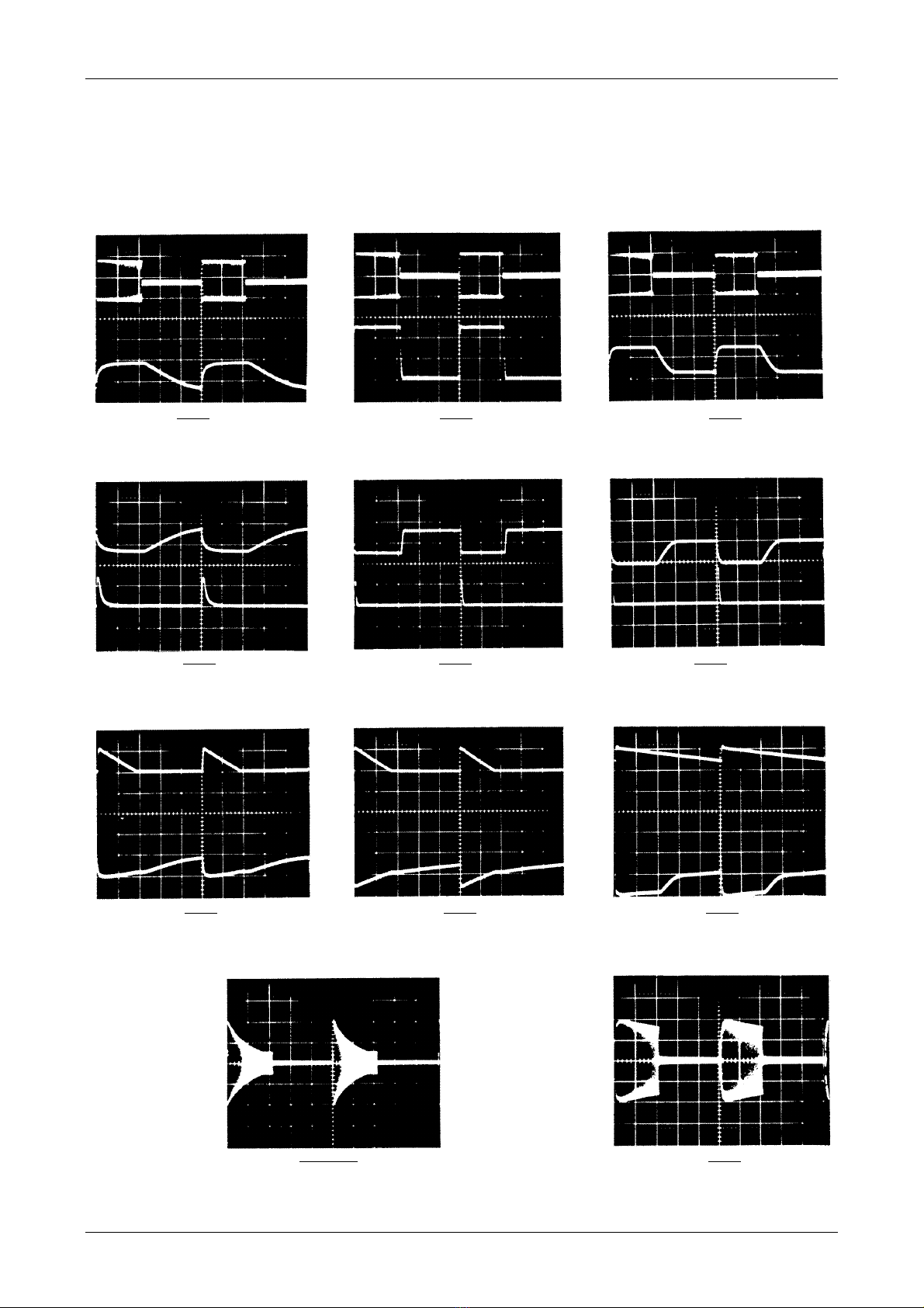
All photos:
All front controls @ maximum;
Rear trim (Impact Release Rate) centred
a&bphotos: c photos;
300 Hz tone-burst @ 316 mV rms (447 mV peak),
128 cycles on, 172 cycles off, 0.2 s/div
3kHz tone-burst @ 316 mV rms (447 mV peak),
128 cycles on, 172 cycles off, 20 ms/div
4.a.1 4.b.1 4.c.1
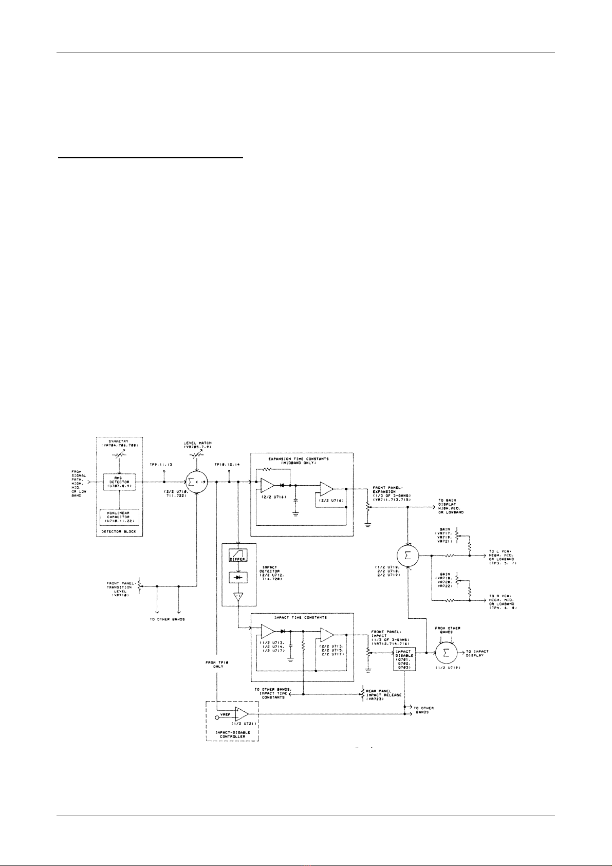
Top: Low-pass filter output, U702L,
pin 1, or U702R, pin 7, 0.2 V/div;
Top: Mid-band summer output, U701L,
pin 7, or U701R, pin 1, 0.5 V/div;
Top: High-pass filter output, U702L,
pin 7, or U702R pin 1, 0.2 V/div;
Bottom: Low-band rms-detector output,
U707, pin 7 (TP9), 0.1 V/div.
Bottom: Mid-band rms-detector output,
U708, pin 7 (TP11), 50 mV/div.
Bottom: High-band rms-detector output,
U709, pin 7 (TP13), 0.1 V/div.
4.a.2 4.b.2 4.c.2
Top: Low-band rms-buffer output,
U710, pin 7 (TP10), 1 V/div;
Top: Mid-band rms-buffer output,
U711, pin 7 (TP12), 1 V/div;
Top: High-band rms-buffer output,
U722, pin 7 (TP14), 1 V/div;
Bottom: Low-band impact-detector
output, U713, pin 5, 0.2 V/div.
Bottom: Mid-band impact-detector
output, U714, pin 3, 0.5 V/div.
Bottom: High-band impact-detector
output, U717, pin 5, 0.2 V/div.
4.a.3 4.b.3 4.c.3
Top: Output, low-band impact time-
constants, U713, pin 1, 1 V/div;
Top: Output. mid-band impact time-
constants, U715, pin 7, 1 V/div;
Top: Output, high-band impact time-
constants, U717, pin 1, 0.5 V/div;
Bottom: Low-band VCA control voltage,
U706L or R, pin 3 (TP3 or 4), 0.1 V/div.
Bottom: Mid-band VCA control voltage,
U705L or R, pin 3 (TP5 or 6), 0.1 V/div.
Bottom: High-band VCA control voltage,
U704L or R, pin 3 (TP7 or 8), 0.1 V/div.
4.a & b.4 4.c.4
Left or right output, 5 V/div Left or right output, 0.5 V/div