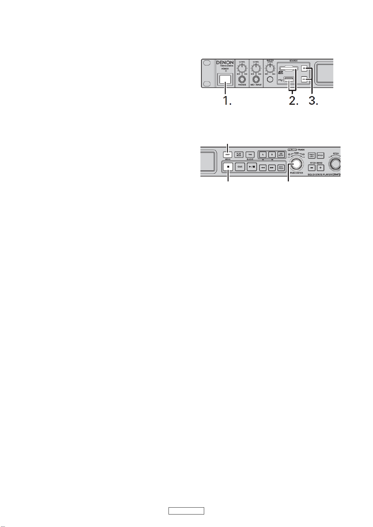
Denon Professional DN-F300 User manual

●For purposes of improvement, specifications and design are subject to change without notice.
●Please use this service manual with referring to the operating instructions without fail.
●Some illustrations using in this service manual are slightly different from the actual set.
X0443 V.01 DE/CDM 0909
SERVICE MANUAL
PROFESSIONAL SOLID STATE PLAYER
MODEL JP E3 E2 EK E2A E2C E1K EUT
DN-F300
33
Ver. 1

2
DN-F300
Please heed the points listed below during servicing and inspection.
◎Heed the cautions!
Spots requiring particular attention when servicing, such
as the cabinet, parts, chassis, etc., have cautions indicated
on labels or seals. Be sure to heed these cautions and the
cautions indicated in the handling instructions.
◎Caution concerning electric shock!
(1) An AC voltage is impressed on this set, so touching in-
ternal metal parts when the set is energized could
cause electric shock. Take care to avoid electric shock,
by for example using an isolating transformer and
gloves when servicing while the set is energized, un-
plugging the power cord when replacing parts, etc.
(2)There are high voltage parts inside. Handle with extra
care when the set is energized.
◎Caution concerning disassembly and
assembly!
Though great care is taken when manufacturing parts from
sheet metal, there may in some rare cases be burrs on the
edges of parts which could cause injury if fingers are
moved across them. Use gloves to protect your hands.
◎Only use designated parts!
The set's parts have specific safety properties (fire resis-
tance, voltage resistance, etc.). For replacement parts, be
sure to use parts which have the same properties. In par-
ticular, for the important safety parts that are marked zon
wiring diagrams and parts lists, be sure to use the desig-
nated parts.
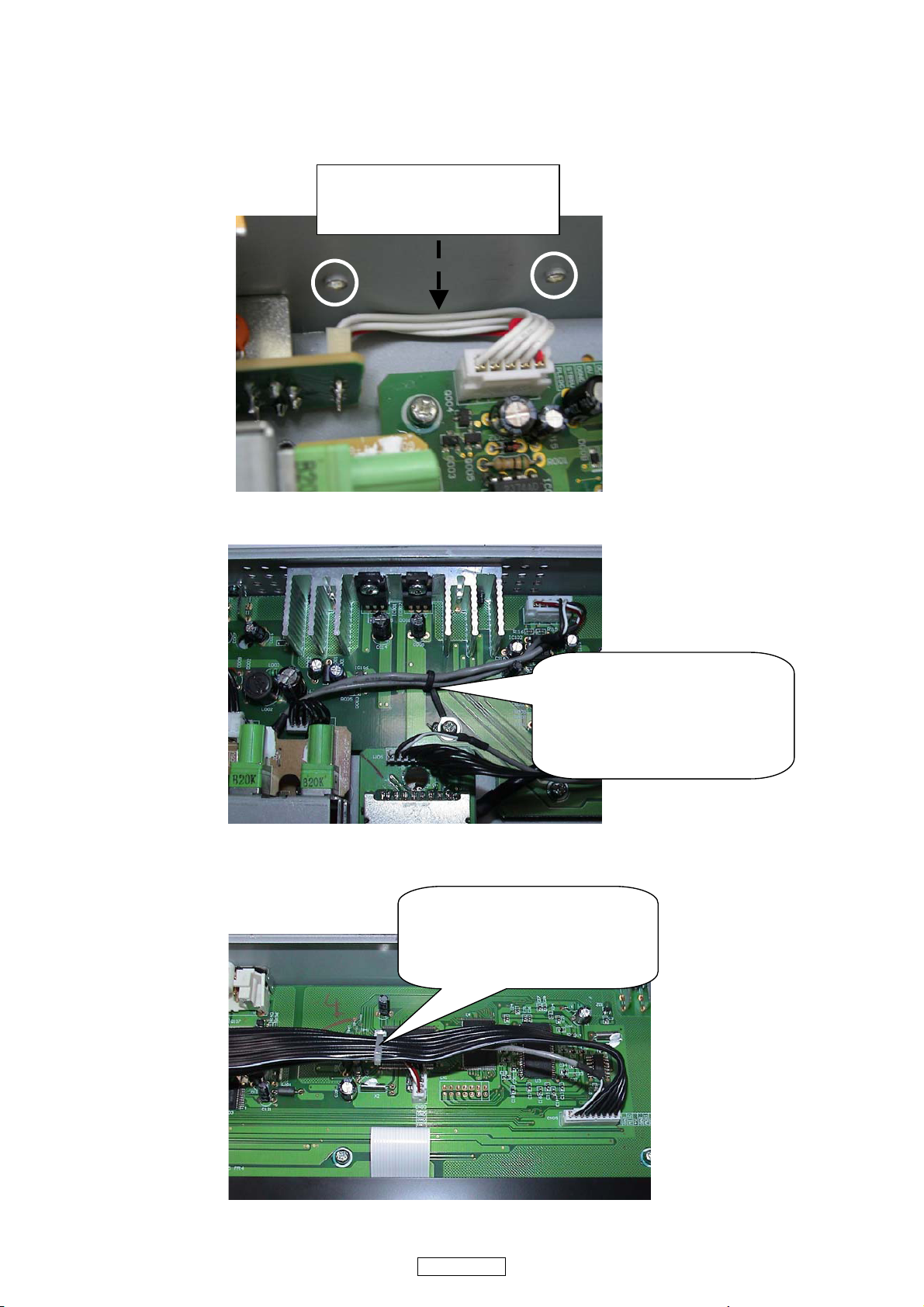
◎Be sure to mount parts and arrange
the wires as they were originally!
For safety reasons, some parts use tape, tubes or other in-
sulating materials, and some parts are mounted away from
the surface of printed circuit boards. Care is also taken with
the positions of the wires inside and clamps are used to
keep wires away from heating and high voltage parts, so
be sure to set everything back as it was originally.
◎Inspect for safety after servicing!
Check that all screws, parts and wires removed or discon-
nected for servicing have been put back in their original po-
sitions, inspect that no parts around the area that has been
serviced have been negatively affected, conduct an insu-
lation check on the external metal connectors and between
the blades of the power plug, and otherwise check that
safety is ensured.
(Insulation check procedure)
Unplug the power cord from the power outlet, disconnect
the antenna, plugs, etc., and turn the power switch on. Us-
ing a 500V insulation resistance tester, check that the in-
sulation resistance between the terminals of the power
plug and the externally exposed metal parts (antenna ter-
minal, headphones terminal, microphone terminal, input
terminal, etc.) is 1MΩor greater. If it is less, the set must
be inspected and repaired.
Concerning important safety
parts
Many of the electric and structural parts used in the set
have special safety properties. In most cases these prop-
erties are difficult to distinguish by sight, and using re-
placement parts with higher ratings (rated power and
withstand voltage) does not necessarily guarantee that
safety performance will be preserved. Parts with safety
properties are indicated as shown below on the wiring dia-
grams and parts lists is this service manual. Be sure to re-
place them with parts with the designated part number.
(1) Schematic diagrams ... Indicated by the zmark.
(2) Parts lists ... Indicated by the zmark.
Using parts other than the designated
parts could result in electric shock, fires or
other dangerous situations.
SAFETY PRECAUTIONS
The following check should be performed for the continued protection of the customer and service technician.
LEAKAGE CURRENT CHECK
Before returning the unit to the customer, make sure you make either (1) a leakage current check or (2) a line to chassis
resistance check. If the leakage current exceeds 0.5 milliamps, or if the resistance from chassis to either side of the
power cord is less than 460 kohms, the unit is defective.
CAUTION
CAUTION

3
DN-F300
DIMENSION
ዧۃʻሽʼڅڶૻֆ

4
DN-F300
WIRE ARRANGEMENT
If wire bundles are untied or moved to perform adjustment or parts replacement etc., be sure to rearrange them neatly as they
were originally bundled or placed afterward.
Otherwise, incorrect arrangement can be a cause of noise generation.
Press the coil down to the cable,pls
be noted to avoid the screw hole
(as round marking)
Fix the 5P line of Jack board firmly
with locking cable clip and keep the
distance with black gict cable as far
as possible,but please take attention
that it cant be closed to above
Fix the 9P line in the SD card board
with the 5P line in the USB board
with cable ties,keep the insulation
line under the flat cable

5
DN-F300
VERSION UPGRADE PROCEDURE OF FIRMWARE
Use the procedure described below to update the firmware to a newer version.
(1) Press the POWER switch to turn on the power.
(2) Insert a SD card or a USB device that has the update file
'dnf30XXX.bin' on the root. Put both files on the SD card or
the USB device if we provide 2 .bin files.
(3) Press the SD or USB[source] button for the input source to
be updated.
※At this time, "V-XX.XXOK?" is displayed in the display sec-
tion. If this is not displayed, perform steps (5 )- (8 )and
check the version.
(4) If the FOLDER/TRACK jog is pressed, "Update" flashes in
the display section, and update begins. When update has
completed, the system automatically restarts.
(5) To check the current main unit version, press the MENU/
STORE button for 2 seconds. At this time, the menu list is
displayed in the display section.
(6) Turn the FOLDER/TRACK jog to select "F/W Version".
(7) If the FOLDER/TRACK jog is pressed, the current version is
displayed in the display section.
(8) Press the STOP button to exit the menu mode.
Note:
Please DO NOT touch and DO NOT disconnect power while the unit is being updated.
Before you update the unit, make sure that the power cable is firmly plugged into the DN-F300 and into an AC outlet.
If the power is turned off accidentally while the unit is being updated, the DN-F300 may not start up.
※Please set the preset menu again after the upgrade.
䎘䎑䎃
8. 6.7.

6
DN-F300
TROUBLE SHOOTING
FLOW CHART NO.1䇭
(
MAIN/POWER UNIT
)
FLOW CHART NO.2 (CONTROL UNIT)
䇭The
p
ower cannot be turned on.
Is the AC ada
p
tor normal䋿㪥㫆
㪰㪼㫊
Is normal state restored when once unplugged
power cord is plu
gg
ed a
g
ain after several seconds?
㪰㪼㫊
㪥㫆
Check if there is any leak or short-circuiting on
the primary or secondly circuit component of
SWITCHING POWER SUPPLY UNIT, and
replace it if defective.
Is the +3.3line volta
g
e normal?
㪰㪼㫊
㪥㫆
Check the the periphery circuit of MAIN and PANEL, and
replace it if defective.
LCD does not dis
p
la
y
.
Is 5V volta
g
e su
pp
lied to 33
p
ins
(
VCC
)
of IC203?
㪰㪼㫊
㪥㫆 Check the +5V line and service it if defective.
Is the +5V line volta
g
e normal? 㪥㫆
Is the USB5 line volta
g
e normal?
䇭Is the A5V line volta
g
e normal?
㪰㪼㫊
㪰㪼㫊
㪰㪼㫊
䇭Is the -A5V line volta
g
e normal?
㪰㪼㫊
㪥㫆
㪥㫆
㪥㫆
Replace the AC adaptor.
Re
p
lace IC203.

7
DN-F300
FLOW CHART NO.3䇭
(
CONTROL UNIT
)
FLOW CHART NO.4䇭(MAIN/POWER UNIT)
䇭The ke
y
o
p
eration is not functionin
g
.
䇭Both functions of
p
icture and sound do not o
p
erate
The WAV file in which test signal of 1kHz/0dB is written is
prepared. With the test signal of 1kHz/0dB it repeats
between B from A and puts in playback state.
Are the audio signals outputted to 26pin(LINE Lch) and
24pin(HP Rch) of IC101, 16pin(LINE Lch) and 13pin(LINE
Rch) of IC103?
㪰㪼㫊
㪥㫆
Check the input signal from IC101, IC103, and
their periphery, and service it if detective.
When the input signal is correct, IC101 or IC103
is replaced.
Are the audio signals outputted to 7pin(HP Lch) and 1pin(HP
Rch) of IC102, 7pin(LINE Lch) and 1pin(LINE Rch) of
IC102?
Check periphery circuit IC102, IC104, and
service it if defective.
When the periphery circuit is correct, IC102 or
IC104 is replaced.
㪰㪼㫊
Is MUTE released, and has been the Q002 base L(0V)? Check Q002 and the periphery circuit, and
service it if defective.
㪰㪼㫊
Check periphery circuit from 7pin and 1pin to JK104, JK102
of IC102, IC104 and replace it if defective.
㪰㪼㫊
㪥㫆
Are the contact point and the installation state of the tact
switches normal?
Re-install the switches correctly or replace the
poor switch.
㪰㪼㫊
㪥㫆
Does LED light correctly ? Check the IC201 and their periphery, and
service it if detective.
㪰㪼㫊
㪥㫆
When pressing each switches, do the voltage of each pin
of IC201(shown below) increase?
Check the switches and their periphery, and
service it if detective.
Re
p
lace IC201.
㪥㫆
㪥㫆

8
DN-F300
SEMICONDUCTORS
Only major semiconductors are shown, general semiconductors etc. are omitted to list.
The semiconductor which described a detailed drawing in a schematic diagram are omitted to list.
1. IC’s
UDA1345TS/N2 (IC101)
ha
lfpage
VSSA(ADC)
VDDA(ADC)
VINL
Vref(A)
VINR
VADCN
VADCP
MC1
MP1
VDDD
VSSD
SYSCLK
MP2
MP3
Vref(D)
VSSO
VOUTL
VDDO
VDDA(DAC)
VSSA(DAC)
VOUTR
MC2
MP5
DATAI
DATAO
WS
BCK
MP4
1
2
3
4
5
6
7
8
9
10
11
12
13
28
27
26
25
24
23
22
21
20
19
18
17
16
1514
UDA1345TS
MGS876
ew
idth
MGS875
ADC
0 dB/6 dB
SWITCH 0 dB/6 dB
SWITCH
3 5
10
11
18
16
17
19
25 27 23 22
12
15
14
13
20
21
8
VINL
VDDD
VSSD
DATAO
BCK
WS
DATAI
MP1
VOUTL
28
24
9
26 VOUTR
SYSCLK
MP4
MP3
MP2
MP5
MC2
MC1
VINR
21 76 4
DECIMATION FILTER
DC-CANCELLATION FILTER
DIGITAL INTERFACE L3-BUS
INTERFACE
ADC
DAC
Vref(D)
VDDO VSSO
DAC
INTERPOLATION FILTER
NOISE SHAPER
VDDA(ADC) VSSA(ADC) VADCP VADCN Vref(A)
UDA1345TS
VDDA(DAC) VSSA(DAC)
SYMBOL PIN TYPE DESCRIPTION
VSSA(ADC) 1 analog ground pad ADC analog ground
VDDA(ADC) 2 analog supply pad ADC analog supply voltage
VINL 3 analog input pad ADC input left
Vref(A) 4 analog pad ADC reference voltage
VINR 5 analog input pad ADC input right
VADCN 6 analog pad ADC negative reference voltage
VADCP 7 analog pad ADC positive reference voltage
MC1 8 5 V tolerant digital input pad with internal pull-down pad mode control 1 (pull-down)
MP1 9 5 V tolerant slew rate controlled digital output pad multi purpose pin 1
VDDD 10 digital supply pad digital supply voltage
VSSD 11 digital ground pad digital ground
SYSCLK 12 5 V tolerant digital Schmitt triggered input pad system clock 256, 384 or 512fs
MP2 13 3-level input pad multi purpose pin 2
MP3 14 5 V tolerant digital Schmitt triggered input pad multi purpose pin 3
MP4 15 3-level input pad multi purpose pin 4
BCK 16 5 V tolerant digital Schmitt triggered input pad bit clock input
WS 17 5 V tolerant digital Schmitt triggered input pad word select input
DATAO 18 5 V tolerant slew rate controlled digital output pad data output
DATAI 19 5 V tolerant digital Schmitt triggered input pad data input
MP5 20 5 V tolerant digital Schmitt triggered input pad multi purpose pin 5 (pull down)
MC2 21 5 V tolerant digital input pad with internal pull-down pad mode control 2 (pull-down)
VSSA(DAC) 22 analog ground pad DAC analog ground
VDDA(DAC) 23 analog supply pad DAC analog supply voltage
VOUTR 24 analog output pad DAC output right
VDDO 25 analog supply pad operational amplifier supply voltage
VOUTL 26 analog output pad DAC output left
VSSO 27 analog ground pad operational amplifier ground
Vref(D) 28 analog pad DAC reference voltage

9
DN-F300
PCM1716E (IC103)
LRCIN
DIN
BCKIN
CLKO
XTI
XTO
DGND
V
DD
V
CC
2R
AGND2R
EXTR
NC
V
OUT
R
AGND1
ML/IIS
MC/DM1
MD/DM0
MUTE
MODE
CS/IWO
RST
ZERO
V
CC
2L
AGND2L
EXTL
NC
V
OUT
L
V
CC
1
1
2
3
4
5
6
7
8
9
10
11
12
13
14
28
27
26
25
24
23
22
21
20
19
18
17
16
15
PCM1716E
PIN NAME I/O DESCRIPTION
1 LRCIN IN Left and Right Clock Input. This clock is equal to
the sampling rate - f
S
.
(1)
2 DIN IN Serial Audio Data Input
(1)
3 BCKIN IN Bit Clock Input for Serial Audio Data.
(1)
4 CLKO OUT Buffered Output of Oscillator. Equivalent to
System Clock.
5 XTI IN Oscillator Input (External Clock Input)
6 XTO OUT Oscillator Output
7 DGND — Digital Ground
8V
DD
— Digital Power +5V
9V
CC
2R — Analog Power +5V
10 AGND2R — Analog Ground
11 EXTR OUT Rch, Common Pin of Analog Output Amp
12 NC — No Connection
13 V
OUT
R OUT Rch, Analog Voltage Output of Audio Signal
14 AGND1 — Analog Ground
15 V
CC
1 — Analog Power +5V
16 V
OUT
L OUT Lch, Analog Voltage Output of Audio Signal
17 NC — No Connection
18 EXTL OUT Lch, Common Pin of Analog Output Amp
19 AGND2L — Analog Ground
20 V
CC
2L — Analog Power +5V
21 ZERO OUT Zero Data Flag
22 RST IN Reset. When this pin is low, the DF and
modulators are held in reset.
(2)
23 CS/IWO IN Chip Select/Input Format Selection. When this
pin is low, the Mode Control is effective.
(3)
24 MODE IN
Mode Control Select. (H: Software, L: Hardware)
(2)
25 MUTE IN Mute Control
26 MD/DM0 IN Mode Control, DATA/De-emphasis Selection 1
(2)
27 MC/DM1 IN Mode Control, BCK/De-emphasis Selection 2
(2)
28 ML/I
2
S IN Mode Control, WDCK/Input Format Selection
(2)
NOTES: (1) Pins 1, 2, 3; Schmitt Trigger input. (2) Pins 22, 24, 25, 26, 27,
28; Schmitt Trigger input with pull-up resister. (3) Pin 23; Schmitt Trigger
input with pull-down resister.
PIN ASSIGNMENTS

10
DN-F300
MC9508AW60 (IC201)
Block Diagram
PTD3/AD1P11/KBI1P6
PTD4/AD1P12/TPM2CLK
PTD5/AD1P13
PTD6/AD1P14/TPM1CLK
PTC1/SDA1
PTC0/SCL1
VSS
VDD
PTE3/TPM1CH1
PTE2/TPM1CH0
PTA7– PTA0
PTE0/TxD1
PTE1/RxD1
PTD2/AD1P10/KBI1P5
PTD1/AD1P9
PTD0/AD1P8
PTC6
PTC5/RxD2
PTC4
PTC3/TxD2
PTC2/MCLK
PORT A
PORT C
PORT D
PORT E
8-BIT KEYBOARD
INTERRUPT MODULE (KBI1)
IIC MODULE (IIC1)
SERIAL PERIPHERAL
INTERFACE MODULE (SPI1)
USER FLASH
USER RAM
DEBUG
MODULE (DBG)
(AW60 = 63,280 BYTES)
HCS08 CORE
CPU
BDC
NOTES:
1. Port pins are software configurable with pullup device if input port.
2. Pin contains software-configurable pullup/pulldown device if IRQ is enabled
(IRQPE = 1). Pulldown is enabled if rising edge detect is selected (IRQEDG = 1)
3. IRQ does not have a clamp diode to VDD. IRQ should not be driven above VDD.
4. Pin contains integrated pullup device.
5. Pins PTD7, PTD3, PTD2, and PTG4 contain both pullup and pulldown devices.
Pulldown enabled when KBI is enabled (KBIPEn = 1) and rising edge is selected
(KBEDGn = 1).
2-CHANNEL TIMER/PWM
MODULE (TPM2)
PTB7/AD1P7–
PORT B
PTE5/MISO1
PTE4/ SS1
PTE6/MOSI1
PTE7/SPSCK1
HCS08 SYSTEM CONTROL
RESETS AND INTERRUPTS
MODES OF OPERATION
POWER MANAGEMENT
VOLTAGE
REGULATOR
RTI COP
IRQ LVD
LOW-POWER OSCILLATOR
INTERNAL CLOCK
GENERATOR (ICG)
RESET
VSSAD
VDDAD
VREFH
ANALOG-TO-DIGITAL
CONVERTER (ADC1)
6-CHANNEL TIMER/PWM
MODULE (TPM1)
PTD7/AD1P15/KBI1P7
8
PTB0/AD1P0
PTG4/KBI1P4
PTG2/KBI1P2
PTG3/KBI1P3
PORT G
AW60/48/32 = 2048 BYTES
10-BIT
BKGD/MS
PTF3/TPM1CH5
PTF2/TPM1CH4
PTF0/TPM1CH2
PTF1/TPM1CH3
PORT F
PTF5/TPM2CH1
PTF4/TPM2CH0
PTF6
PTF7
INTERFACE MODULE (SCI1)
SERIAL COMMUNICATIONS
INTERFACE MODULE (SCI2)
SERIAL COMMUNICATIONS
PTG0/KBI1P0
PTG1/KBI1P1
(AW48 = 49,152 BYTES)
(AW32 = 32,768 BYTES)
VREFL
PTG5/XTAL
PTG6/EXTAL
IRQ
RxD2
TxD2
SDA1
SCL1
AD1P15–AD1P8
AD1P7–AD1P0
KBI1P4–KBI1P0
KBI1P7–KBI1P5
TPM2CH1–TPM2CH0
TPM2CLK
SPSCK1
SS1
MISO1
MOSI1
TPM1CLK
TPM1CH5–
RxD1
TxD1
EXTAL
XTAL
8
8
5
3
2
(AW16 = 16,384 BYTES)
AW16 = 1024 BYTES
8
TPM1CH0 6

11
DN-F300
ST7066-0B (IC203)
Block Diagram
Timing
Generator
16-bit
shift
registe
r
Common
Signal
Driver
Display
data RAM
(DDRAM)
80x8 bits
40-bit
latch
circuit
Segment
Signal
Driver
40-bit
shift
registe
r
LCD Drive
Voltage
Selector
CPG
Instruction
Register (IR)
Instruction
Decoder
Reset
Circuit
MPU
Interface
Input/
Output
Buffer
Address
Counter
Character
generator
ROM
(CGROM)
9,920 bits
Character
generator
RAM
(CGRAM)
64 bits
Cursor
and
Blink
controller
Data
Register
(DR)
Busy
Flag
Parallel/Serial converter
and
Attribute Circuit
GND
Vcc
V1 V2 V3 V4 V5
OSC1 OSC2 CL1
CL2
M
D
COM1 to
COM16
SEG1 to
SEG40
RS
RW
E
DB4 to
DB7
DB0 to
DB3

12
DN-F300
ADSP-BF532 (U1)
Block Diagram
M29W800B70N6 (U4)
SP
SEQUENCER
ALIGN
DECODE
LOO P BUF FER
DAG0 DA G 1
16 16
88 8 8
40 40
A0 A1
BARREL
SHIFTER
DATA ARITHME TIC UNIT
CONTROL
UN IT
ADDRESS ARITHMETIC UNIT
FP
P5
P4
P3
P2
P1
P0
I3
I2
I1
I0
L3
L2
L1
L0
B3
B2
B1
B0
M3
M2
M1
M0
LD032BITS
LD132BITS
SD 3 2 BI TS
R7.L
R6.L
R5.L
R4.L
R3.L
R2.L
R1.L
R0.L
R7 .H
R6 .H
R5 .H
R4 .H
R3 .H
R2 .H
R1 .H
R0 .H
R7
R6
R5
R4
R3
R2
R1
R0
DQ3
DQ9
DQ2
A6 DQ0
W
A3
RB
DQ6
A8
A9 DQ13
A17
A10 DQ14
A2
DQ12
DQ10
DQ15A–1
VCC
DQ4
DQ5
A7
DQ7
NC
NC
AI02179
M29W800T
M29W800B
(Normal)
12
1
13
24 25
36
37
48
DQ8
NC
NC
A1
A18
A4
A5
DQ1
DQ11
G
A12
A13
A16
A11
BYTE
A15
A14 VSS
E
A0
RP
VSS
A0-A18 Address Inputs
DQ0-DQ7 Data Input/Outputs, Command Inputs
DQ8-DQ14 Data Input/Outputs
DQ15A–1 Data Input/Output or AddressInput
E Chip Enable
G Output Enable
W Write Enable
RP Reset / Block TemporaryUnprotect
RB Ready/Busy Output
BYTE Byte/Word Organisation
VCC Supply Voltage
VSS Ground

13
DN-F300
ADSP-BF532 (U3)
Block Diagram
VDD
N.C
VDDQ
N.C
DQ0
VSSQ
N.C
N.C
VDDQ
N.C
DQ1
VSSQ
N.C
VDD
N.C
WE
CAS
RAS
CS
BA0
BA1
A10/AP
A0
A1
A2
A3
VDD
1
2
3
4
5
6
7
8
9
10
11
12
13
14
15
16
17
18
19
20
21
22
23
24
25
26
27
54
53
52
51
50
49
48
47
46
45
44
43
42
41
40
39
38
37
36
35
34
33
32
31
30
29
28
VSS
N.C
VSSQ
N.C
DQ3
VDDQ
N.C
N.C
VSSQ
N.C
DQ2
VDDQ
N.C
VSS
N.C/RFU
DQM
CLK
CKE
N.C
A11
A9
A8
A7
A6
A5
A4
VSS
C O SC O
VDD
DQ0
VDDQ
N.C
DQ1
VSSQ
N.C
DQ2
VDDQ
N.C
DQ3
VSSQ
N.C
VDD
N.C
WE
CAS
RAS
CS
BA0
BA1
A10/AP
A0
A1
A2
A3
VDD
VSS
DQ7
VSSQ
N.C
DQ6
VDDQ
N.C
DQ5
VSSQ
N.C
DQ4
VDDQ
N.C
VSS
N.C/RFU
DQM
CLK
CKE
N.C
A11
A9
A8
A7
A6
A5
A4
VSS
VDD
DQ0
VDDQ
DQ1
DQ2
VSSQ
DQ3
DQ4
VDDQ
DQ5
DQ6
VSSQ
DQ7
VDD
LDQM
WE
CAS
RAS
CS
BA0
BA1
A10/AP
A0
A1
A2
A3
VDD
VSS
DQ15
VSSQ
DQ14
DQ13
VDDQ
DQ12
DQ11
VSSQ
DQ10
DQ9
VDDQ
DQ8
VSS
N.C/RFU
UDQM
CLK
CKE
N.C
A11
A9
A8
A7
A6
A5
A4
VSS
x16 x8 x4 x16
x8x4
54Pin TSOP
(400mil x 875mil)
(0.8 mm Pin pitch)
Bank Select
Data Input Register
8M x 4 / 4M x 8 / 2M x 16
Sense AMP
Output BufferI/O Control
Column Decoder
Latency & Burst Length
Programming Register
Address Register
Row Buffer
Refresh Counter
Row Decoder Col. Buffer
LRAS
LCBR
LCKE
LRAS LCBR LWE LDQM
CLK CKE CS RAS CAS WE L(U)DQM
LWE
LDQM
DQi
CLK
ADD
LCAS LWCBR
8M x 4 / 4M x 8 / 2M x 16
Timing Register

14
DN-F300
ISP1761BE (U6)
Block Diagram
XTAL1
XTAL2
11
12
CLKIN
13
BUS INTERFACE:
MEMORY
MANAGEMENT
UNIT
+
SLAVE DMA
CONTROLLER
+
INTERRUPT
CONTROL
HC BUFFER
MEMORY
64 KBYTES
MEMORY ARBITER
AND FIFO
TRANSACTION
TRANSLATOR
(TT) AND RAM
OTG CONTROLLER
004aaa450
PLL
30 MHz
60 MHz
GLOBAL CONTROL
AND POWER
MANAGEMENT
DIGITAL
AND ANALOG
OVERCURRENT
PROTECTION
D[15:0]/D[31:0]
GENERIC PROCESSOR BUS
SEL16/32
REGISTERS
SUPPORT
DC BUFFER
MEMORY
8 KBYTES
ADVANCED
PHILIPS
SLAVE HOST
CONTROLLER
ADVANCED
PERIPHERAL
CONTROLLER
DYNAMIC PORT ROUTING AND PORT CONTROL LOGIC
ID
37 to 39, 41 to 43,
45 to 47, 49, 51,
52, 54, 56 to 58,
60 to 62, 64 to 66,
68 to 70, 72 to 74,
76 to 78, 80
82, 84, 86, 87,
89, 91 to 93,
95 to 98,
100 to 103, 105
106
CS_N 107
RD_N
108
WR_N
112
HC_IRQ 113
DC_DREQ
111
DC_IRQ
V
CC(I/O)
10, 40, 48, 59, 67,
75, 83, 94, 104, 115
ISP1761
RESET_N
HC_SUSPEND
/
WAKEUP_N
122
119
DC_SUSPEND
/
WAKEUP_N
120
GND
4, 8, 14, 17, 24,
31, 36, 44, 53,
55, 63, 71, 79,
88, 90, 99, 109,
121, 123
POWER-ON
RESET AND
V
BAT
ON
5 V-TO-1.8 V
VOLTAGE
REGULATOR V
CC(5V0)
V
BAT_ON_N
5 V-TO-3.3 V
VOLTAGE
REGULATOR V
REG(3V3)
V
REG(1V8)
9
6, 7
110
5, 50,
85, 118
REF5V
2
HI-SPEED
USB ATX1
DP1 DM1
PSW1_N
OC1_N/
V
BUS
PSW2_N
OC2_N
PSW3_N
OC3_N
HI-SPEED
USB ATX2 HI-SPEED
USB ATX3
DP2 DM2 DP3 DM3
20 18 27 25
21 127
19
GND
26
GND
28 128 34 32
33
GND
35 1
RREF1
16
GND
15
RREF2
23
GND
22
RREF3
30
GND
29
3
116
HC_DACK 117
DC_DACK
114
HC_DREQ
CHARGE
PUMP
124
C_B
C_A 125
126
VCC(C_IN)
A[17:1]
17

15
DN-F300
BLOCK DIAGRAM
DSP
ROMRAM
UI CPU
LCD DRIVER
LCD
3 1
2
VR
KEY, ENCODER
M29W800DBK 4S281632F
ST7066U
P OWER SUP P L Y
5V
3.3V
LED
-5V
SD CARD
SLOT
AMP
4580
AUDIO OUT
ADSP -BF 532
MC9S08AW60
USB(HOST)
ISP-1761
USB IF
1 2
4580
AMP
L
3
G
1
MI C2 I N
L
3
R
2
G
1
P HONES
4556
AMP
CODEC
DAC
UDA1345TS
P CM1716
REMOTE
SENSOR
CONTROL PWB
MAIN PWB
1
P OWER SW.
USB5V
STB5V
AMP
4580 L
3
G
1
MI C1 I N
1
2
3
DC I N
EEP ROM
AT93C46

16
DN-F300
LEVEL DIAGRAM
0dBV
-10dBV
-20dBV
-30dBV
-40dBV
-50dBV
-60dBV
-70dBV
-80dBV
10dBV
-90dBV
INPUT IN PUT OPAMP OUT PUT OPAMP
HEADPHONE OUTPUT(-1.72dB)
DSP (CODEC & DAC) OUT PUT
UNBALANCED OUTPUT(6dB)
MIC1 & MIC2 INPUT(-38dB)
USB & SD INPUT(0dB)
MASTER VR
HEADPHONE VR
MIC1 & MIC2 VR

17
DN-F300
PRINTED WIRING BOARDS
I/O PWB UNIT
USB PWB UNIT POWER SW PWB UNIT SD CARD PWB UNIT
COMPONENT SIDE
FOIL SIDE
COMPONENT SIDECOMPONENT SIDE
FOIL SIDE
COMPONENT SIDE
FOIL SIDE
COMPONENT SIDE
FOIL SIDE

18
DN-F300
CONTROL PWB UNIT
JACK PWB UNIT VR PWB UNIT
COMPONENT SIDE
FOIL SIDE
COMPONENT SIDECOMPONENT SIDECOMPONENT SIDECOMPONENT SIDE
COMPONENT SIDE
FOIL SIDE
FOIL SIDE

19
DN-F300
NOTE FOR PARTS LIST
Parts for which "nsp" is indicated on this table cannot be supplied.
When ordering of part, clearly indicate "1" and "I" (i) to avoid mis-supplying.
Ordering part without stating its part number can not be supplied.
Not including General-purpose Carbon Chip Resistor in the P.W.Board parts list. (Refer to the Schematic Diagram for those parts.)
Parts marked with this symbol zhave critical characteristics.
Use ONLY replacement parts recommended by the manufacturer.
Not including General-purpose Carbon Film Resistor in the P.W.Board parts list. (Refer to the Schematic Diagram for those parts.)
Part indicated with the mark "★" is not illustrated in the exploded view.
WARNING:
1.
2.
3.
4.
5.
6.
●Resistors
RD : Carbon
RC : Composition
RS : Metal oxide film
RW: winding
RN : Metal film
RK : Metal mixture
P : Pulse-resistant type
NL : Low noise type
NB : Non-burning type
FR : Fuse-resistor
F : Lead wire forming
2B : 1/8 W
2E : 1/4 W
2H : 1/2 W
3A : 1 W
3D : 2 W
3F : 3 W
3H : 5 W
F:±1%
G:±2%
J:±5%
K:±10%
M:±20%
Ex.: RN
Type
14K
Shape
and per-
formance
2E
Power
182
Resist-
ance
G
Allowable
error
FR
Others
*Resistance
1800ohm=1.8kohm18 2
Indicates number of zeros after effective number.
2-digit effective number.
1.2ohm1R 2
2-digit effective number, decimal point indicated by R.
1-digit effective number.
: Units: ohm
●Capacitors
CE : Aluminum foil
electrolytic
CA : Aluminium solid
electrolytic
CS : Tantalum electrolytic
CQ : Film
CK : Ceramic
CC : Ceramic
CP : Oil
CM: Mica
CF : Metallized
CH : Metallized
HS : High stability type
BP : Non-polar type
HR : Ripple-resistant type
DL : For change and discharge
HF : For assuring high requency
U : UL part
C : CSA part
W : UL-CSA part
F : Lead wire forming
0J : 6.3 V
1A : 10 V
1C : 16 V
1E : 25 V
1V : 35 V
1H : 50 V
2A : 100 V
2B : 125 V
2C : 160 V
2D : 200 V
2E : 250 V
2H : 500 V
2J : 630 V
F:±1%
G:±2%
J:±5%
K:±10%
M:±20%
Z:±80%
: - 20%
P : +100%
C:±0.25pF
D:±0.5pF
= : Others
Ex.: CE
Type
04W
Shape
and per-
formance
1H
Dielectric
strength
3R2
Capacity
M
Allowable
error
BP
Others
・Units:μF.
2200μF22 2
Indicates number of zeros after effective number.
2-digit effective number.
・Units:μF.
2.2μF2R 2
2-digit effective number, decimal point indicated by R
1-digit effective number.
*Capacity (electrolyte only)
・When the dielectric strength is indicated in AC,"AC" is included after the dieelectric strength value.
*Capacity (except electrolyte)
・Units:pF
2200pF=0.0022μF22 2
Indicates number of zeros after efective number.
(More than 2)
2-digit effective number.
・Units:pF
220pF22 1
2-digit effective number.
Indicates number of zeros after effective numver.
(0 or 1)

20
DN-F300
PARTS LIST OF P.W.B. UNIT
*Parts for which "nsp" is indicated on this table cannot be supplied.
*The parts listed below are for maintenance only, might differ from the parts used in the unit in appearances or dimensions.
I/O PWB ASS'Y
Ref. No. Part No. Part Name Remarks Q'ty New
SEMICONDUCTORS GROUP
IC001 00MHC3690521F IC (BA05T,3PIN)
417-CDN34A-314
IC002 941239001610S IC (BA033T/FP 3.3V TO220FP 3PIN)
417-HV3500K-253
IC003,004 941239002820P IC (BA05CCOWFP-E2 SMD-5P)
417-PDJ1-865
*
IC005 941239002800P IC (NJM-2374AD,DIP-8)
417-ID-829
*
IC101 941239002830P IC (UDA1345TS/N2)
417-SA12-490
*
IC102 00D9580073804 IC (NJM4556AD)
417-3113-018
IC103 00D2622490902 IC (PCM1716E,28PIN)
417-DCM270X-327A
IC104,IC105 00D9587058602 IC (NJM4580D)
417-HDJ2400-318
IC106 00D9410045601 IC (BD4745G/BD4745G-TR)
417-HDJ2000-503
Q001,002 90M-BA001610R CHIP TRANSISTOR (DTA124TKAT146)
416-HDJ9700-210
Q003 00MHX327121A0 TRANSISTOR (2SC2712-GR,2-3F1A)
416-CTB200-166
Q004 941219002720S TRANSISTOR (DTA114TKA,SMT3)
416-S300-327
*
Q005 00D9410046503 TRANSISTOR (DTC124EKAT146)
416-CDN88-044
Q1,2 941219002740S TRANSISTOR (RTR030P02TL,TSMT3)
416-UDJ200-347
*
Q101-110 00D9410046406 TRANSISTOR (2SC4695)
416-DAIA-273
D002 941209002670S DIODE (1N5819(GW))
414-DFX1-144
*
D003 00D9410046901 SWITCHING DIODE (1SS355,UMD2)
414-CD1000-075
D005-009 00D9410046901 SWITCHING DIODE (1SS355,UMD2)
414-CD1000-075
U1 941239002850P IC (ADSP-BF532)
417-SDJ2-814
*
U3 941239002840P IC (K4S281632I-UC75)
417-SDJ2-813
*
U4 941243003040P BUFFER IC ASS'Y
(M29W800B70N6.SMD)
704-F300-8688
U5 941239002790P IC (FDS9431A)
417-G350-770
*
U6 941239002860P IC (ISP1761BE)
417-UDJ1-882
*
U7 00D9580076209 IC (74HC04)
417-DCM370E3-378
ZD1 941209002700S DIODE (ZHCS1000/RB491DT146)
414-G350-216
*
ZD002 941209002690S DIODE
414-F300-293
*
RESISTORS GROUP
R2 nsp CHIP RESISTOR (1K OHM,1/10W,J,TP,50V)
412-CDVD2001-540
R11 nsp CHIP RESISTOR ((47 OHM,1/10W,J,TP ,50V)
412-007USB-697
R12-14 nsp CHIP RESISTOR (220 OHM,1/10W,J,TP 50V)
412-CDVD2001-521
R15 nsp CHIP RESISTOR (4.7K OHM,1/10W,J,TP,50V)
412-CDVD2001-523
R16 nsp CHIP RESISTOR (10K OHM,1/10W,J,TP ,50V)
412-CDVD2001-534
R17 nsp CHIP RESISTOR (220 OHM,1/10W,J,TP 50V)
412-CDVD2001-521
R18,19 nsp CHIP RESISTOR (10K OHM,1/10W,J,TP ,50V)
412-CDVD2001-534
R21-27 nsp CHIP RESISTOR (10K OHM,1/10W,J,TP ,50V)
412-CDVD2001-534
R26 nsp CHIP RESISTOR (220 OHM,1/10W,J,TP 50V)
412-CDVD2001-521
R28-30 nsp CHIP RESISTOR (12K OHM,1/10W,J,TP ,50V)
412-007USB-702
R31 nsp CHIP RESISTOR (10K OHM,1/10W,J,TP ,50V)
412-CDVD2001-534
R34,35 nsp CHIP RESISTOR (10K OHM,1/10W,J,TP ,50V)
412-CDVD2001-534
R36-43 nsp CHIP RESISTOR (220 OHM,1/10W,J,TP 50V)
412-CDVD2001-521
R44 nsp CHIP RESISTOR (22 OHM,1/10W,F,TP ,50V)
412-CDVD2001-554
R45,46 nsp CHIP RESISTOR (220 OHM,1/10W,J,TP 50V)
412-CDVD2001-521
R001 nsp
CARBON FILM RESISTOR (0.5OHM,1/4W,J,T-52/BOX)
412-UDJ3E-1342
Table of contents