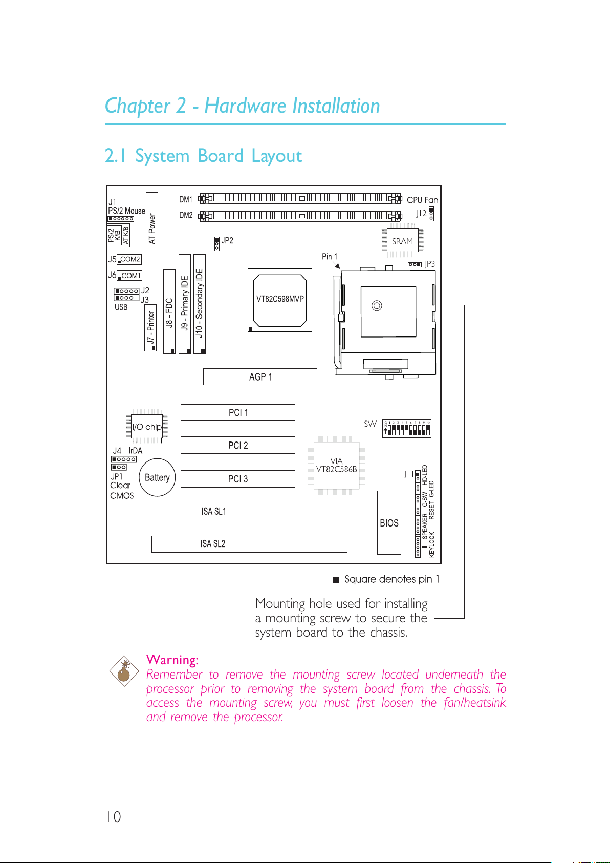
DFI P5BV3+/e User manual

P5BV3+/e
Rev. A+
System Board
Users Manual
36411913
All manuals and user guides at all-guides.com
all-guides.com

Copyright
This publication contains information that is protected by copyright. No
part of it may be reproduced in any form or by any means or used to
make any transformation/adaptation without the prior written permission
from the copyright holders.
This publication is provided for informational purposes only. The
manufacturer makes no representations or warranties with respect to
the contents or use of this manual and specifically disclaims any express
or implied warranties of merchantability or fitness for any particular purpose.
The user will assume the entire risk of the use or the results of the use of
this document.Further,the manufacturer reserves the right to revise this
publication and make changes to its contents at any time, without obligation
to notify any person or entity of such revisions or changes.
All Rights Reserved. © 1999
Trademarks
Microsoft®MS-DOS®, WindowsTM, Windows®95 and Windows®98
are registered trademarks of Microsoft Corporation. Intel, Pentium
and Pentium with MMX technology are registered trademarks of
Intel Corporation. Cyrix, 6x86L, 6x86MX and M II are registered
trademarks of Cyrix Corporation. AMD, K5, K6, K6-2 and K-III are
registered trademarks of Advanced Micro Devices, Inc. IBM 6x86MX
is a registered trademark of International Business Machine
Corporation. IDT C6, WinChip2 and WinChip3 are registered
trademarks of IDT Corporation. Award is a registered trademark of
Award Software, Inc. Other trademarks and registered trademarks
of products appearing in this manual are the properties of their
respective holders.
Caution:
Danger of explosion if battery incorrectly replaced.
Replace only with the same or equivalent type recommended by the
manufacturer.
Dispose of used batteries according to the battery manufacturers
instructions.
All manuals and user guides at all-guides.com

FCC and DOC Statement on Class B
This equipment has been tested and found to comply with the limits
for a Class B digital device, pursuant to Part 15 of the FCC rules.
These limits are designed to provide reasonable protection against
harmful interference when the equipment is operated in a residential
installation. This equipment generates, uses and can radiate radio
frequency energy and, if not installed and used in accordance with
the instruction manual, may cause harmful interference to radio
communications. However, there is no guarantee that interference
will not occur in a particular installation. If this equipment does cause
harmful interference to radio or television reception, which can be
determined by turning the equipment off and on, the user is
encouraged to try to correct the interference by one or more of the
following measures:
Reorient or relocate the receiving antenna.
Increase the separation between the equipment and the receiver.
Connect the equipment into an outlet on a circuit different from
that to which the receiver is connected.
Consult the dealer or an experienced radio TV technician for
help.
Notice:
1. The changes or modifications not expressly approved by the
party responsible for compliance could void the user's authority
to operate the equipment.
2. Shielded interface cables must be used in order to comply with
the emission limits.
All manuals and user guides at all-guides.com

Table of Contents
Chapter 1 - Introduction
1.1 Features and Specifications......................................................................
1.2 Package Checklist .........................................................................................
Chapter 2 - Hardware Installation
2.1 System Board Layout .................................................................................
2.2 System Memory .............................................................................................
2.3 DIP Switch Settings of the Processors ............................................
2.4 Jumper Settings for Clearing CMOS Data. ...................................
2.5 Jumper Settings for SDRAM Clock (DIMM) ................................
2.6 Connecting the Ribbon Cables and Wires of the Ports
and Connectors .............................................................................................
Chapter 3 - Award BIOS Setup Utility
3.1 The Basic Input/Output System ...........................................................
3.1.1 Standard CMOS Setup .............................................................
3.1.2 BIOS Features Setup ..................................................................
3.1.3 Chipset Features Setup .............................................................
3.1.4 Power Management Setup ......................................................
3.1.5 PNP/PCI Configuration .............................................................
3.1.6 Load Fail-Safe Settings ...............................................................
3.1.7 Load Optimal Settings ..............................................................
3.1.8 Integrated Peripherals .................................................................
3.1.9 Supervisor Password ..................................................................
3.1.10 User Password ...............................................................................
3.1.11 IDE HDD Auto Detection .....................................................
3.1.12 Save & Exit Setup ........................................................................
3.1.13 Exit Without Saving .....................................................................
6
9
28
28
31
35
36
38
40
40
41
44
45
45
46
46
10
11
11
18
19
20
All manuals and user guides at all-guides.com

54
54
56
Chapter 4 - Supported Softwares
4.1 Desktop Management Interface .........................................................
4.2 Drivers ...............................................................................................................
Appendix A - Identifying Processors
A.1 Intel Processors .............................................................................................
A.2 Cyrix Processors ..........................................................................................
A.3 IBM Processors .............................................................................................
A.4 AMD Processors .........................................................................................
A.5 IDT Processors .............................................................................................
Appendix B - System Error Messages
B.1 POST Beep .....................................................................................................
B.2 Error Messages ..............................................................................................
Appendix C - Troubleshooting
C.1 Troubleshooting Checklist ........................................................................
47
50
51
51
52
52
53
All manuals and user guides at all-guides.com

6
1.1 Features and Specifications
1.1.1 Features
Chipset
VIAApollo 598MVP AGP system chipset
Processor
The system board is equipped with a 321-pin ZIF socket (Super
Socket 7). It is alos equipped with a switching voltage regulator that
supports 2.0V to 3.5V core voltage for various processors.
AMD®K5 PR90/PR100/PR120/PR133/PR166, K6-166/200/233/
266/300, K6-2/250/266/300/333/350/366/380/400/450 or K6-
III/400
Intel Pentium90/100/120/133/150/166/200MHz or Intel
Pentiumprocessor with MMXTM technology-166/200/233MHz
Cyrix®6x86L PR150+/PR166+/PR200+, 6x86MX-PR166/
PR200/PR233/PR266 or M II-200/266/300/333/366/380/400
IBM® 6x86MX-PR200/PR233/PR266/PR300/PR333
IDT®C6-180/200/225/240, WinChip2-200/225/233/240/266/
300 or future WinChip3 series
System Memory
16MB to 256MB memory using unbuffered DIMMs
Two 168-pin DIMM sockets using x64 SDRAM, 3.3V
PC-100 SDRAM DIMM for 100MHz external system bus clock
processors
Chapter 1 - Introduction
DIMMs
2MBx64
4MBx64
8MBx64
16MBx64
Memory Size
16MB
32MB
64MB
128MB
All manuals and user guides at all-guides.com
all-guides.com

7
1
Introduction
Level 2 Cache Memory
512KB pipeline burst, direct map write-through cache installed on
the system board.
Expansion Slots
The system board is equipped with 1 dedicated AGP slot. AGP is an
interface designed to support high performance 3D graphics cards. It
utilizes a dedicated pipeline to access system memory for texturing,
z-buffering and alpha blending; delivering up to 533MB/sec.
bandwidth for 3D graphics applications. AGP in this system board
will deliver faster and better graphics with your PC.
The system board is equipped with 1 dedicated AGP slot, 2
dedicated PCI slots, 1 dedicated 16-bit ISA slot and 1 shared PCI/
ISA slot. All PCI and ISA slots are bus masters.
Desktop Management Interface (DMI)
The system board comes with a DMI 2.0 built into the BIOS. The
DMI utility in the BIOS automatically records various information
about your system configuration and stores these information in the
DMI pool, which is a part of the system board's Plug and Play
BIOS. DMI, along with the appropriately networked software, is
designed to make inventory, maintenance and troubleshooting of
computer systems easier. Refer to Chapter 4 for instructions on
using the DMI utility.
Connectors
2 connectors for external USB ports
1 connector for IrDA interface
2 serial ports
1 parallel port
2 IDE connectors
1 floppy connector
1 PS/2 mouse port
1 PS/2 or AT keyboard port
1 12-pin standard AT power supply connector
1 fan connector for CPU fan
All manuals and user guides at all-guides.com

8
Introduction
1
PCI Bus Master IDE Controller
Two PCI IDE interfaces support up to four IDE devices
Ultra DMA/33 supported (Synchronous Ultra DMA mode -
data transfer rate up to a maximum of 33MB/sec.)
PIO Mode 3 and Mode 4 Enhanced IDE (data transfer rate up
to 16.6MB/sec.)
Bus mastering reduces CPU utilization during disk transfer
ATAPI CD-ROM, LS-120, ZIP supported and SCSI sequential
boot-up.
IrDA Interface
The system board is equipped with an IrDA connector for wireless
connectivity between your computer and peripheral devices. It
supports infrared peripheral devices that meet the ASKIR or HPSIR
standard.
USB Ports
The system board is equipped with two connectors for external
USB ports. USB allows data exchange between your computer and
a wide range of simultaneously accessible external Plug and Play
peripherals.
BIOS
Award BIOS, Windows95/98 Plug and Play compatible
Flash EPROM for easy BIOS upgrades
1MB flash memory (2MB - optional, includes SDMS function)
1.1.2 Intelligence
Virus Protection
Most viruses today destroy data stored in hard drives. The system
board is designed to protect the boot sector and partition table of
your hard disk drive.
All manuals and user guides at all-guides.com

9
1
Introduction
1.2 Package Checklist
The system board package contains the following items:
þThe system board
þA users manual
þSerial, mouse and printer port cables
Option 1:
- One card-edge bracket with a 9-pin and 25-pin serial port
cables
- One card-edge bracket with a 25-pin printer port cable and
a PS/2 mouse port cable
Option 2:
- One card-edge bracket with two 9-pin serial port cables
and a PS/2 mouse port cable
- One 25-pin printer port cable for chassis mounting
þOne 40-pin IDE hard disk cable
þOne 34-pin floppy disk drive cable
þOne CD
¨One card-edge bracket with two USB ports (optional)
If any of these items are missing or damaged, please contact your
dealer or sales representative for assistance.
All manuals and user guides at all-guides.com

10
2.1 System Board Layout
Chapter 2 - Hardware Installation
Mounting hole used for installing
a mounting screw to secure the
system board to the chassis.
Warning:
Remember to remove the mounting screw located underneath the
processor prior to removing the system board from the chassis. To
access the mounting screw, you must first loosen the fan/heatsink
and remove the processor.
All manuals and user guides at all-guides.com

11
2
Hardware Installation
2.2 System Memory
2.3 DIP Switch Settings of the Processors
Make sure SW1 and JP3 are set correctly before applying power or
you may damage the processor or system board. There are 10
switches on SW1. The black rectangle in the diagram denotes the
part that is protruding, the adjustable switch.
Important:
If you are using a 100MHz ex-
ternal system bus clock
processor, make sure that you
use PC-100 SDRAM DIMM
ONLY. Just in case you
encounter compatibility problems,
we recommend that you try
setting the SDRAM clock
according to the AGP clock (JP2
pins 1 and 2 On). This may help
solve some compatibility
problems.
In the example on the left:
Switch 1: Off Switch 6: Off
Switch 2: On Switch 7: Off
Switch 3: On Switch 8: Off
Switch 4: On Switch 9: Off
Switch 5: On Switch 10: On
All manuals and user guides at all-guides.com
all-guides.com

12
2Hardware Installation
DIP Switch Settings for Intel Processors
Intel Processors SW1: 1-6
90MHz -
60MHz - 1.5x
100MHz -
66MHz - 1.5x
120MHz -
60MHz - 2x
133MHz -
66MHz - 2x
150MHz -
60MHz - 2.5x
166MHz -
66MHz - 2.5x
200MHz -
66MHz - 3x
MMX166MHz* -
66MHz - 2.5x
MMX200MHz -
66MHz - 3x
MMX233MHz -
66MHz - 3.5x
Intel Processors SW1: 1-6
* Default
DIP Switch Settings for IDT Processors
C6-180 - 60MHz - 3x
C6-200 - 66MHz - 3x
IDT Processors SW1: 1-6 IDT Processors SW1: 1-6
C6-225 - 75MHz - 3x
WinChip2-266 -
100MHz - 2.33x
C6-240 - 60MHz - 4x
WinChip2-300 -
100MHz - 2.5x
WinChip2-200 -
66MHz - 3x
WinChip2-225 -
75MHz - 3x
WinChipP2-240 -
60MHz - 4x
WinChip2-233 -
66MHz - 3.5x
All manuals and user guides at all-guides.com

13
2
Hardware Installation
DIP Switch Settings for IBM Processors
IBM Processors SW1: 1-6 IBM Processors SW1: 1-6
6x86MX-PR200 -
66MHz - 2.5x
6x86MX-PR233 -
75MHz - 2.5x
6x86MX-PR266 -
83MHz - 2.5x
6x86MX-PR300 -
75MHz - 3x
6x86MX-PR333 -
83MHz - 3x
6x86MX-PR300 -
66MHz - 3.5x
DIP Switch Settings for Cyrix Processors
Cyrix Processors SW1: 1-6 Cyrix Processors SW1: 1-6
6x86MX-PR200 -
66MHz - 2.5x
6x86MX-PR233 -
75MHz - 2.5x
6x86MX-PR266 -
83MHz - 2.5x
M II-300 -
75MHz - 3x
M II-333 -
83MHz - 3x
M II-400 -
95MHz - 3.5x
M II-300 -
66MHz - 3.5x
6x86L PR150+ -
60MHz - 2x
6x86L PR166+ -
66MHz - 2x
6x86MX-PR166 -
60MHz - 2.5x
6x86L PR200+ -
75MHz - 2x
M II-200 -
66MHz - 2.5x
M II-266 -
66MHz - 3x
M II-333 -
66MHz - 4x
M II-333 -
75MHz - 3.5x
M II-366 -
100MHz - 2.5x
M II-366 -
83MHz - 3.5x
M II-380 -
100MHz - 3x
All manuals and user guides at all-guides.com

14
2Hardware Installation
DIP Switch Settings for AMD Processors
AMD Processors SW1: 1-6 AMD Processors SW1: 1-6
K6-200 -
66MHz - 3x
K6-233 -
66MHz - 3.5x
K6-266 -
66MHz - 4x
K6-300 -
66MHz - 4.5x
K6-2/250 -
100MHz - 2.5x
K6-2/300 -
100MHz - 3x
K6-2/333 -
95MHz - 3.5x
K6-2/350 -
100MHz - 3.5x
K6-2/400 -
100MHz - 4x
K5 PR90 -
60MHz - 1.5x
K5 PR100 -
66MHz - 1.5x
K5 PR120 -
60MHz - 2x
K5 PR133 -
66MHz - 2x
K5 PR166 -
66MHz - 2.5x
K6-166 -
66MHz - 2.5x
K6-2/333 -
66MHz - 5x
K6-2/366 -
66MHz - 5.5x
K6-2/380 -
95MHz - 4x
K6-2/300 -
66MHz - 4.5x
K6-2/450 -
100MHz - 4.5x
K6-III/400 -
100MHz - 4x
K6-2/266 -
66MHz - 4x
All manuals and user guides at all-guides.com

15
2
Hardware Installation
External System Bus Clock / Frequency Ratio - DIP Switch Settings
If the processor you are using is not included in the previous tables,
please refer to the following tables and set SW1 according to the
external system bus clock and frequency ratio of your processor.
External System Bus Clock Settings
External System Bus Clock SW1: 1-3
60MHz
External System Bus Clock SW1: 1-3
66MHz
75MHz
83MHz
95MHz
100MHz
Warning:
We do not guarantee that 75MHz, 83MHz, 95MHz and
100MHz external system bus clock processors will work with all
types of add-in cards, memory modules or other devices.
Frequency Ratio SW1: 4-6
1.5x / 3.5x
Frequency Ratio SW1: 4-6
2x
2.5x
4x
4.5x
5x
3x 5.5x
Frequency Ratio Settings for Intel, IBM, Cyrix and AMD
Processors
All manuals and user guides at all-guides.com

16
2Hardware Installation
Frequency Ratio SW1: 4-6
3.5x
Frequency Ratio SW1: 4-6
2x/3.3x
2.5x
4x
4.5x
2.33x/5x
3x 2.66x/5.5x
Frequency Ratio Settings for IDT Processors
All manuals and user guides at all-guides.com
all-guides.com

17
2
Hardware Installation
DIP Switch and Jumper Settings for Core Voltage
Voltage JP3 SW1: 7-10
2.8V*
2.0V
2.1V 2.9V
3.0V
3.1V
Voltage JP3 SW1: 7-10
2.2V
2.3V
2.4V
2.5V
2.6V
2.7V
3.2V
3.3V
3.4V
3.5V
* Default
All manuals and user guides at all-guides.com

18
2Hardware Installation
2-3 On: Normal
(default)
1-2 On:
Clear CMOS Data
2.4 Jumper Settings for Clearing CMOS Data
Jumper JP1
Clear CMOS Data
If, for some reason, the CMOS
data becomes corrupted, the
system can be reconfigured
with the default values stored
in the ROM BIOS.To load the
default values, power off your
system. Set JP1 pins 1 and 2
to On.Wait for a few seconds
and set JP1 back to its default
setting, pins 2 and 3 On. You
may now power-on your
system.
All manuals and user guides at all-guides.com

19
2
Hardware Installation
2.5 Jumper Settings for SDRAM Clock (DIMM)
Jumper JP2
SDRAM Clock
JP2 is used to set the SDRAMs
clock according to the CPU
clock or AGP clock. If you are
using PC SDRAM DIMMs, it is
recommended that you set the
SDRAM clock according to the
CPU clock (2-3 On).This setting
will provide better system
performance specially when used
with 75/83/95/100MHz
processors. However, if you
encounter compatibility problems
with PC-100 SDRAM DIMMs or you are using EDO/PC-66
SDRAM DIMMs, set the SDRAM clock according to the AGP clock
(1-2 On).
2-3 On:
SDRAM CLK = CPU CLK
1-2 On:
SDRAM CLK = AGP CLK
(default)
CPU CLK
60MHz
66MHz
75MHz
83MHz
95MHz
100MHz
SDRAM CLK
60MHz
66MHz
60MHz
66MHz
66MHz
66MHz
AGP CLK
60MHz
66MHz
60MHz
66MHz
66MHz
66MHz
CPU CLK
60MHz
66MHz
75MHz
83MHz
95MHz
100MHz
SDRAM CLK
60MHz
66MHz
75MHz
83MHz
95MHz
100MHz
AGP CLK
60MHz
66MHz
60MHz
66MHz
66MHz
66MHz
1
2
3
1
2
3
All manuals and user guides at all-guides.com

20
2Hardware Installation
2.6 Connecting the Ribbon Cables and Wires of
the Ports and Connectors
2.6.1 Serial Ports
The built-in serial ports are RS-232C asynchronous communication
ports with 16C550A-compatible UARTs that can be used with
modems, serial printers, remote display terminals, and other serial
devices. You can set the serial ports I/O address in the Integrated
Peripherals setup of the Award BIOS.
Connecting the Serial Ports
Two serial port cables
mounted on a card-edge
bracket are provided with the
system board. Connect one
serial port cable to connector
J6 for COM 1 primary serial
port and the other serial port
cable to connector J5 for the
COM 2 secondary serial port.
Make sure the colored stripes
on the ribbon cables are
aligned with pins 1 of
connectors J5 and J6. Mount
the card-edge bracket to the
system chassis.
All manuals and user guides at all-guides.com
Other manuals for P5BV3+/e
2
Table of contents
Other DFI Motherboard manuals