Diodes AP22913 Installation and operating instructions

AP22913-EVM
Application Note
AP22913 Application Information and Demo Board User Guide
This application note contains new product information. Diodes, Inc. reserves the right to modify the product specification without notice. No liability is
assumed as a result of the use of this product. No rights under any patent accompany the sale of the product.
1/8
Rev. A February 2020
www.diodes.com Diodes Incorporated
Description
The AP22913 slew rate controlled load switch is a
single P-channel MOSFET power switch designed
for high-side load-switching applications. The
MOSFET has a typical RDS(ON) of 54mat
5V(X1-WLB0909-4), allowing increased load current
handling capacity with a low forward voltage drop.
The turn-on slew rate of the device is controlled
internally. VIN and VOUT are isolated during OFF state
with TRCB (True Reverse Current Blocking) feature.
The AP22913 load switch is designed to operate
from 1.4V to 5.5V, making it ideal for 1.8V, 2.5V, 3.3V,
and 5V systems. The typical quiescent supply
current is only 1µA.
The AP22913 is available in the wafer level chip
scale 4-pin, X1-WLB0909-4 0.5mm pitch package.
Applications
Mobile Device and Smart Phones
Portable Media Devices
Wearable Devices
Advanced Notebook, UMPC and MID
Portable Medical Devices
GPS and Navigation Equipment
Features
Wide Input Voltage Range: 1.4V to 5.5V
Low On-Resistance(X1-WLB0909-4):
92mΩ Typical @1.5V
76mΩ Typical @1.8V
56mΩ Typical @3.3V
54mΩ Typical @5.0V
High DC Current Capability up to 2A
Truly Reverse Current Block (TRCB)
Discharging Resistor on VOUT When Disabled
Ultra Low Quiescent Current 1µA
Active-high Control Pin
Minimum 1.1V VIH of ON
ESD Protection:
Human Body Model: 2kV
Charged Device Model: 1kV
Totally Lead-Free & Fully RoHS compliant
(Notes 1 & 2)
Halogen and Antimony Free. “Green” Device
(Note 3)
Notes:
1. No purposely added lead. Fully EU Directive 2002/95/EC
(RoHS), 2011/65/EU (RoHS 2) & 2015/863/EU (RoHS 3)
compliant.
2. See https://www.diodes.com/quality/lead-free/ for more
information about Diodes Incorporated’s definitions of
Halogen- and Antimony-free, "Green" and and Lead-free.
3. Halogen- and Antimony-free "Green” products are defined as
those which contain <900ppm bromine, <900ppm chlorine
(<1500ppm total Br + Cl) and <1000ppm antimony
compounds.

AP22913-EVM
Application Note
AP22913 Application Information and Demo Board User Guide
This application note contains new product information. Diodes, Inc. reserves the right to modify the product specification without notice. No liability is
assumed as a result of the use of this product. No rights under any patent accompany the sale of the product.
2/8
Rev. A February 2020
www.diodes.com Diodes Incorporated
Typical Applications Circuit
AP22913
VIN
ON GND
VOUT
VIN VOUT
CIN
1μF
COUT
0.1μF~1μF
Absolute Maximum Ratings
Symbol
Parameter
Ratings
Unit
ESD HBM
Human Body Model ESD Protection
6
kV
ESD CDM
Charged Device Model ESD Protection
2
kV
VIN
Input Voltage
-0.3 to 6
V
VOUT
Output Voltage
-0.3 to 6
V
VON
ON Voltage
-0.3 to 6
V
ILOAD
Maximum Continuous Load Current
2
A
ILOAD
Maximum Pulse Load Current, Pulse <300µs, 2% Duty
Cycle
2.5
A
TJ
Maximum Junction Temperature
+125
°C
TST
Storage Temperature Range
-65 to +150
°C
PD
Power Dissipation
WLB0909-4
735
mW
RθJA
Thermal Resistance, Junction to Ambient (Note 4)
WLB0909-4
136
°C/W
RθJC
Thermal Resistance, Junction to Case (Note 5)
WLB0909-4
31
°C/W

AP22913-EVM
Application Note
AP22913 Application Information and Demo Board User Guide
This application note contains new product information. Diodes, Inc. reserves the right to modify the product specification without notice. No liability is
assumed as a result of the use of this product. No rights under any patent accompany the sale of the product.
3/8
Rev. A February 2020
www.diodes.com Diodes Incorporated
Recommended Operating Conditions
Symbol
Parameter
Min
Max
Unit
VIN
Input Voltage
1.4
5.5
V
VON
ON Voltage Range
0
5.5
V
VOUT
Output Voltage
1.4
5.5
V
IOUT
Output Current
0
2.0
A
VIH
ON High-Level Input Voltage
1.1
5.5
V
VIL
ON Low-Level Input
Voltage
VIN = 3.6V to 5.5V
0
0.6
V
VIN = 1.4V to 3.6V
0
0.4
V
TA
Operating Ambient Temperature
-40
+85
°C
Evaluation Board
Top View
Dimensions: 53.34mm(L) x 43.82 mm(w)

AP22913-EVM
Application Note
AP22913 Application Information and Demo Board User Guide
This application note contains new product information. Diodes, Inc. reserves the right to modify the product specification without notice. No liability is
assumed as a result of the use of this product. No rights under any patent accompany the sale of the product.
4/8
Rev. A February 2020
www.diodes.com Diodes Incorporated
Quick Start Guide
AP22913 is a single p-channel MOSFET load switch. It has an input voltage range between 1.4V to
5.5V and is capable of handling up to 2A continuous current. The board demonstrates the AP22913’s
current handling capacity with its controlled turn on, low RDS(on) and very low quiescent current specification.
All inputs and output are brought out to test points for control and monitoring. All passive components are
included on the EVM for device operation.
1. Connect a power supply between IN and GND terminals.
2. Connect the positive connection to the IN and the negative connection to the GND.
3. Connect an adjustable current or resistive load to OUT and GND terminals.
4. Connect the positive connection of the load to the OUT and the negative connection to the GND.
5. IN via reserved resistor R1 connect to ON terminal or installed shorting jumper on J1 in either the Hi or Lo
positions. The default is shorted directly between IN and ON terminals.
6. Turn on the power supply.
7. Increase the load current of OUT and observe that the load current stop increasing after reaching limit
level.
Evaluation Board Schematic
AP22913CN4
GND2
11
U1
LDSW (X1-WLB0909-4)
B1
A1
B2
A2
GND
VOUT
ON
VIN
VIN_S1
1
C4
nc
GND3
11
J1
ON
1
32
IN 1
1
GND11
1
C2
nc
C1
1u
C3
0.1u
OUT
11
R1
10k
GND41
1
ON
1
1
VOUT_S
11

AP22913-EVM
Application Note
AP22913 Application Information and Demo Board User Guide
This application note contains new product information. Diodes, Inc. reserves the right to modify the product specification without notice. No liability is
assumed as a result of the use of this product. No rights under any patent accompany the sale of the product.
5/8
Rev. A February 2020
www.diodes.com Diodes Incorporated
PCB Layout
Top Side
Bottom Side
X1-WLB0909-4
X1-WLB0909-4
Bill of Materials
Component
Location
Q'ty
Value
Specification
Vendor
Part No.
Size
U1
1
AP22913
2A single channel
load switch
Diodes
AP22913CCN4-7
WLCSP-4
C1
1
1μF
X7R 10% 25V
Cap MLCC
Taiyo Yuden
TMK212B7105KG
0805
C3
1
0.1μF
X7R 10% 50V
Cap MLCC
Taiyo Yuden
UMK212B7104KG
0805
C2,C4
2
-
NC
-
-
-
R1
1
10kΩ
0603 ±1% 1/10W
Resistor
Yageo
RC0603FR-0710KL
0603
PCB
1
AP22913 EV Board
Diodes Inc.
TDB0327
-

AP22913-EVM
Application Note
AP22913 Application Information and Demo Board User Guide
This application note contains new product information. Diodes, Inc. reserves the right to modify the product specification without notice. No liability is
assumed as a result of the use of this product. No rights under any patent accompany the sale of the product.
6/8
Rev. A February 2020
www.diodes.com Diodes Incorporated
Vendors of peripheral components
Suggested Capacitors:
Vendor
Application
Value
Capacitance
Type
Series
Taiyo Yuden
Cin
Cout
1μF
25V/X7R,10%
SMD
TMK212B7105KG
SMD
TMK107B7105KA
Cout
0.1μF
25V/X7R, 20%
SMD
TWK107B7104MV
50V/X7R, 10%
SMD
UMK212B7104KG
Murata
Cin
Cout
1μF
25V/X7R,10%
SMD
GRM21BR71E105KA99
Cout
0.1μF
25V/X7R, 10%
SMD
GRM188R71E104KA01
SMD
GRM21BR71E104KA01
Suggested Resistor:
Vendor
Type
Series
Yageo
SMD
RC0603FR

AP22913-EVM
Application Note
AP22913 Application Information and Demo Board User Guide
This application note contains new product information. Diodes, Inc. reserves the right to modify the product specification without notice. No liability is
assumed as a result of the use of this product. No rights under any patent accompany the sale of the product.
7/8
Rev. A February 2020
www.diodes.com Diodes Incorporated
VOUT Turn On/Off Response Example (CH1: VON, CH2: VOUT)

AP22913-EVM
Application Note
AP22913 Application Information and Demo Board User Guide
This application note contains new product information. Diodes, Inc. reserves the right to modify the product specification without notice. No liability is
assumed as a result of the use of this product. No rights under any patent accompany the sale of the product.
8/8
Rev. A February 2020
www.diodes.com Diodes Incorporated
IMPORTANT NOTICE
DIODES INCORPORATED MAKES NO WARRANTY OF ANY KIND, EXPRESS OR IMPLIED, WITH REGARDS TO THIS DOCUMENT,
INCLUDING, BUT NOT LIMITED TO, THE IMPLIED WARRANTIES OF MERCHANTABILITY AND FITNESS FOR A PARTICULAR
PURPOSE (AND THEIR EQUIVALENTS UNDER THE LAWS OF ANY JURISDICTION).
Diodes Incorporated and its subsidiaries reserve the right to make modifications, enhancements, improvements, corrections or other
changes without further notice to this document and any product described herein. Diodes Incorporated does not assume any liability
arising out of the application or use of this document or any product described herein; neither does Diodes Incorporated convey any
license under its patent or trademark rights, nor the rights of others. Any Customer or user of this document or products described herein
in such applications shall assume all risks of such use and will agree to hold Diodes Incorporated and all the companies whose products
are represented on Diodes Incorporated website, harmless against all damages.
Diodes Incorporated does not warrant or accept any liability whatsoever in respect of any products purchased through unauthorized sales
channel.
Should Customers purchase or use Diodes Incorporated products for any unintended or unauthorized application, Customers shall
indemnify and hold Diodes Incorporated and its representatives harmless against all claims, damages, expenses, and attorney fees
arising out of, directly or indirectly, any claim of personal injury or death associated with such unintended or unauthorized application.
Products described herein may be covered by one or more United States, international or foreign patents pending. Product names and
markings noted herein may also be covered by one or more United States, international or foreign trademarks.
This document is written in English but may be translated into multiple languages for reference. Only the English version of this
document is the final and determinative format released by Diodes Incorporated.
LIFE SUPPORT
Diodes Incorporated products are specifically not authorized for use as critical components in life support devices or systems without the
express written approval of the Chief Executive Officer of Diodes Incorporated. As used herein:
A. Life support devices or systems are devices or systems which:
1. are intended to implant into the body, or
2. support or sustain life and whose failure to perform when properly used in accordance with instructions for use provided in the
labeling can be reasonably expected to result in significant injury to the user.
B. A critical component is any component in a life support device or system whose failure to perform can be reasonably expected to
cause the
failure of the life support device or to affect its safety or effectiveness.
Customers represent that they have all necessary expertise in the safety and regulatory ramifications of their life support devices or
systems, and acknowledge and agree that they are solely responsible for all legal, regulatory and safety-related requirements concerning
their products and any use of Diodes Incorporated products in such safety-critical, life support devices or systems, notwithstanding any
devices- or systems-related information or support that may be provided by Diodes Incorporated. Further, Customers must fully
indemnify Diodes Incorporated and its representatives against any damages arising out of the use of Diodes Incorporated products in
such safety-critical, life support devices or systems.
Copyright © 2020, Diodes Incorporated
www.diodes.com
This manual suits for next models
1
Table of contents
Popular Computer Hardware manuals by other brands

Pico Macom
Pico Macom MOR-CS Specifications

ekwb
ekwb EK-FC 6970 V2 INSTALLATION AND MOUNTING MANUAL
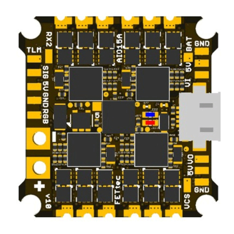
FETtec
FETtec Mini AIO 15A manual
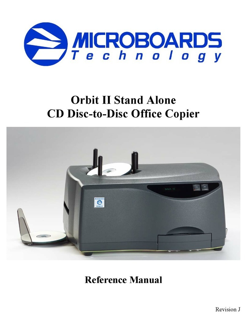
MicroBoards Technology
MicroBoards Technology Orbit II Stand Alone Reference manual

Socket
Socket Pentium 4 Full Size PICMG CPU Card IB810 user manual
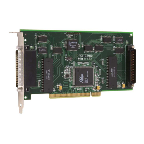
Measurement Computing
Measurement Computing PCI-CTR10 user guide
