Diodes ZETEX ZXLD1370EV2 User manual
Issue 2 – July 2010 www.diodes.com
© Diodes Incorporated, 2010
ZXLD1370EV2 BUCK/BOOST LED DRIVER
USER GUIDE
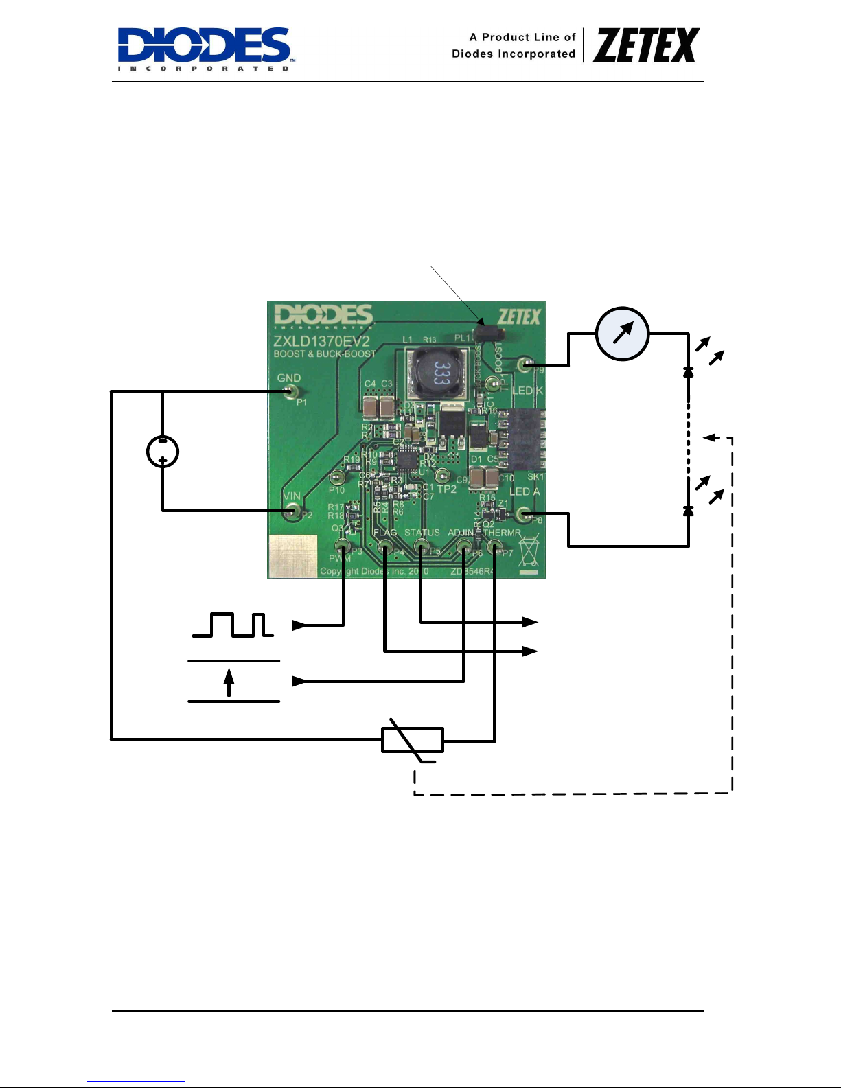
Fig.1 ZXLD1370EV2 Evaluation board connection diagram
8-48V 2A
DC PSU
0-1.5A DC
DVM
BUCK/BOOST
1 - 15 LEDs
1.5A
0V
4.5V
Open Drain output
125mV = 10%
2.5V = 200%
-t°
GND
0 – 4.5V Status steps
Thermal connection

ZXLD1370EV2
Issue 2 – July 2010 www.diodes.com
© Diodes Incorporated 2010
2
Fig2. Schematic diagram
FLAG
ZXLD1370EV2
Issue 2 – July 2010 www.diodes.com
© Diodes Incorporated 2010
3
PARTS LIST
Ref Value Package Part Number Manufacturer Contact Details
U1 LED Driver
Controller TSSOP16L ZXLD1370 Diodes Zetex www.diodes.com
Q1 60V N-ch
MOSFET DPAK DMN6068LK3 Diodes Zetex www.diodes.com
Q2 Q3 60V General
Purpose
Mosfet
SOT23 2N7002 Diodes www.diodes.com
D1 Freewheeling
diode 3A
100V
PowerDI5 PDS3100 Diodes www.diodes.com
D2 51V 200mW
Zener Diodes
SOD323 BZT52C51 Diodes www.diodes.com
D3 Freewheeling
diode 3A
100V
PowerDI5 PDS3100 Diodes www.diodes.com
Z1 47V 300mW
Zener Diode SOT23 BZX84C47 Diodes www.diodes.com
L1 33uH 2.3A MS1246-333MLB
NPIS24H330MTRF
744-7715330
Coilcraft
NIC Comps.
Wurth
www.coilcraft.com
www.niccomp.com
www.we-
online.com
C1 100pF 10V 0805 Generic
C2 C5 C8 1uF 100V
X7R 1206 GRM31CR72A105KA01L Murata www.murata.com
C3 C4 C9
C10 2.2uF 100V
X7R 1812 GRM43ER72A225KA01L Murata www.murata.com
C6 C7 Not fitted
C11 10nF 100V
X7R 0805 Generic
R1 R2 0R3 1206 Generic
R4 1K3 0805 Generic
R7 47K 0805 Generic
R9 120K 1% 0805 Generic
R10 36K 1% 0805 Generic
R3 R5 R6
R8 R11
R12 R14
0R 0805 Generic
R15 2K 0805 Generic
R13 R18 Not fitted
R16 R17
R19 1K 0805 Generic

ZXLD1370EV2
Issue 2 – July 2010 www.diodes.com
© Diodes Incorporated 2010
4
NOTES
The PCB is supplied with R3 and R8 0R0 resistors fitted.
The ‘ADJ’ pin and the ‘TADG’ pin are disabled.
Boost-only mode is selected by changing PL1
In boost mode, the total LED output voltage is <=47V.
The supply voltage for the ZXLD1370EV2 is >=6V, <= (total LED voltage).
In buck-boost operation, the input voltage range is limited by the overvoltage threshold voltage and the
LED voltage. >=6V, <=(47V – VLED).
For other reference designs or further applications information, please refer to the ZXLD1370
datasheet.
Q2 and Z1 protect the circuit from open-circuit LEDs.
The overvoltage threshold of the evaluation board is 47V. (Set by the 47V Zener diode Z1)
The overvoltage threshold can be increased by using a Zener diode with a higher voltage (56V)
Do not use a Zener diode of higher voltage than the MosFet or ZXLD1370.
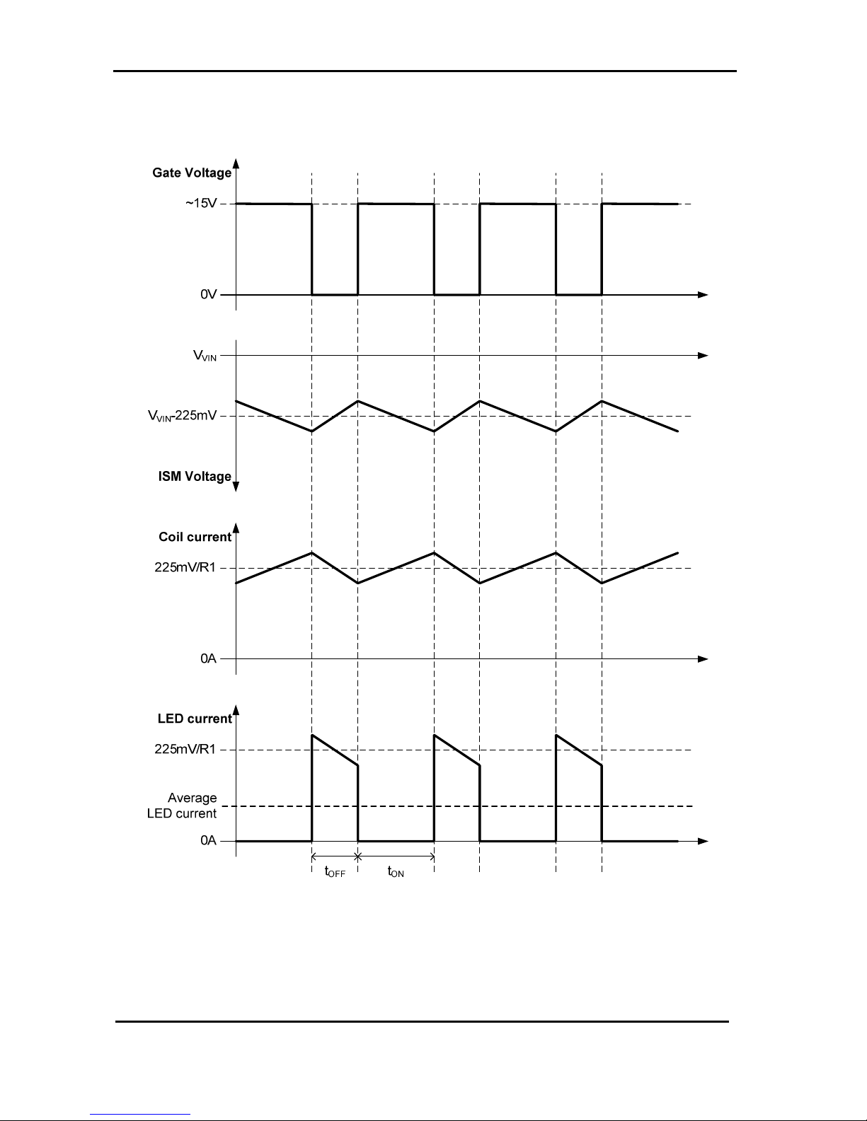
Boost and Buck-boost modes, average I
LED
= average I
INDUCTOR
x R10/(R9+R10)
OPERATION
In Boost and Buck-boost mode the LED current is sensed by the series resistor (R1 // R2). An output
from the control loop drives the input of a comparator. The comparator drives the gate of the external
NMOS switch transistor via ‘GATE’. When the NMOS switch is on, current flows from VIN, via (R1 //
R2), inductor and switch to ground and increases until a high value is reached. Then, GATE goes low,
the switch turns off and the current flows through (R1 // R2), the inductor, D1 and the LED, to ‘VIN’
(Buck-boost mode), or ‘GND’ (Boost mode). When the inductor current has gone low, ‘GATE’ goes high,
and the cycle of events repeats. The circuit oscillates. The average current in the LEDs is equal to the
average of the maximum and minimum threshold currents. The ripple current (hysteresis) is equal to the
difference between the thresholds. The average current in the LED is always less than the average
current in the inductor and the ratio between these currents is set by the values of resistors R9 and
R10. The peak current in the LED is equal to the peak current in the inductor. The control loop keeps
the average LED current at the level set by the voltage on the ‘ADJ’ pin. Loop compensation is
achieved by C1.
Bootstrap Circuit
The ZXLD1370 works normally between 8-60V. For input voltages between 6-8V and high switch
currents that require a fully enhanced MOSFET, it is recommended to use the bootstrap network D2-
R13 and remove R11.
ZXLD1370EV2
Issue 2 – July 2010 www.diodes.com
© Diodes Incorporated 2010
5
Fig. 3 Waveforms for Boost and Buck-boost modes

ZXLD1370EV2
Issue 2 – July 2010 www.diodes.com
© Diodes Incorporated 2010
6
ADJ Terminal (DC output current adjustment)
On the ZXLD1370EV2, the ‘ADJ’ pin R3 connects the internal 1.25V reference (V
REF
) give 100% LED
current.
The ADJ pin can also be driven with an external DC voltage >=125mV and <= 2.5V to adjust the LED
current to >= 10% and <=200% of the nominal value.
To do this, remove R3, fit R5 and apply an external DC voltage between ‘ADJIN’ and ‘GND’
The voltage V
ADJ
can be derived from a resistor-divider connected between ‘REF’ and ‘GND’.
‘ADJ’ has high impedance within its normal operating voltage range. An internal 2.6V clamp protects the
device against excessive input voltage and limits the maximum output current to approximately 4% above
the maximum current set by ‘V
ADJ
‘ if the maximum input voltage is exceeded.
PWM Terminal (PWM output current control/dimming)
The LED current can be adjusted digitally, by applying a low frequency PWM logic signal to the ‘PWM’ pin
to turn the controller on and off. This will produce an average output current proportional to the duty cycle of
the control signal. During PWM operation, the device remains powered up and only the output switch is
switched by the control signal.
The device can be shut down by taking the PWM pin to < 0.4V with a short to 0V or suitable open collector
NPN, or open drain NMOS transistor, for >15ms. In the shutdown state, most of the circuitry inside the
device is off and the quiescent current will be typically 90µA.
TADJ Terminal (Thermal control of LED current)
The ‘Thermal control’ circuit monitors the voltage on the ‘TADJ’ pin and reduces the output current linearly
if the voltage on ‘TADJ’ < 625mV. An NTC thermistor and resistor can be connected to set the voltage on
the ‘TADJ’ pin = 625mV at the required threshold temperature. This will give 100% LED current below the
threshold temperature and <100% above it as shown in the graph. The temperature threshold can be
changed by adjusting the value of Rth and/or the thermistor to suit the LED used.
On the ZXLD1370EV2, Rth is 1K3 (R4). In order to use thermal control, remove R8, fit R6, and fit a 10K
NTC Negative Temperature Coefficient) type thermistor between ‘TADJ’ and ‘GND’. This will set the
threshold temperature to ~ 90ºC.
Thermal control by LED current reduction
Fig. 4 Thermal control
The Thermal Control feature can be disabled by connecting TADJ to REF through the jumper resistor R8.
ZXLD1370EV2
Issue 2 – July 2010 www.diodes.com
© Diodes Incorporated 2010
7
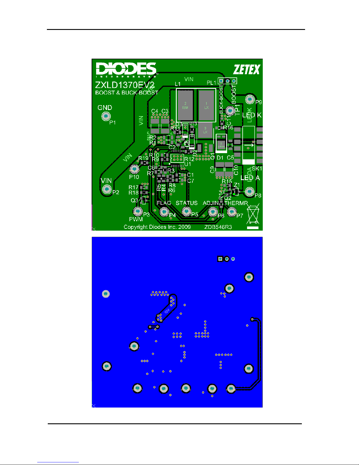
BOARD LAYOUT

ZXLD1370EV2
Issue 2 – July 2010 www.diodes.com
© Diodes Incorporated 2010
8
Sales offices
The Americas
3050 E. Hillcrest Drive
Westlake Village,
CA 91362-3154
Tel: (+1) 805 446 4800
Fax: (+1) 805 446 4850
Europe
Kustermannpark
Balanstraße 59,
D-81541 München
Germany
Tel: (+49) 894 549 490
Fax: (+49) 894 549 4949
Taiwan
7F, No. 50,
Min Chuan Road
Hsin-Tien
Taipei, Taiwan
Tel: (+886) 289 146 000
Fax: (+886) 289 146 639
Shanghai
Rm. 606, No.1158
Changning Road
Shanghai, China
Tel: (+86) 215 241 4882
Fax (+86) 215 241 4891
Shenzhen
Room A1103-04,
ANLIAN Plaza, #4018
Jintian Road
Futian CBD,
Shenzhen, China
Tel: (+86) 755 882 849 88
Fax: (+86) 755 882 849 99
Korea
6 Floor, Changhwa B/D,
1005-5 Yeongtong-dong,
Yeongtong-gu, Suwon-si,
Gyeonggi-do, Korea 443-813
Tel: (+82) 312 731 884
Fax: (+82) 312 731 885
IMPORTANT NOTICE
DIODES INCORPORATED MAKES NO WARRANTY OF ANY KIND, EXPRESS OR IMPLIED, WITH REGARD TO THIS
DOCUMENT, INCLUDING, BUT NOT LIMITED TO, THE IMPLIED WARRANTIES OF MERCHANTABILITY AND
FITNESS FOR A PARTICULAR PURPOSE (AND THEIR EQUIVALENTS UNDER THE LAWS OF ANY JURISDICTION).
Diodes Incorporated and its subsidiaries reserve the right to make modifications, enhancements, improvements,
corrections or other changes without further notice to this document and any product described herein. Diodes Incorporated
does not assume any liability arising out of the application or use of this document or any product described herein; neither
does Diodes Incorporated convey any license under its patent or trademark rights, nor the rights of others. Any Customer
or user of this document or products described herein in such applications shall assume all risks of such use and will agree
to hold Diodes Incorporated and all the companies whose products are represented on Diodes Incorporated website,
harmless against all damages.
Diodes Incorporated does not warrant or accept any liability whatsoever in respect of any products purchased through
unauthorized sales channels. Should Customers purchase or use Diodes Incorporated products for any unintended or
unauthorized application, Customers shall indemnify and hold Diodes Incorporated and its representatives harmless
against all claims, damages, expenses, and attorney fees arising out of, directly or indirectly, any claim of personal injury or
death associated with such unintended or unauthorized application.
Products described herein may be covered by one or more United States, international or foreign patents pending. Product
names and markings noted herein may also be covered by one or more United States, international or foreign trademarks.
LIFE SUPPORT
Diodes Incorporated products are specifically not authorized for use as critical components in life support devices or
systems without the express written approval of the Chief Executive Officer of Diodes Incorporated. As used herein:
A. Life support devices or systems are devices or systems which:
1. are intended to implant into the body, or
2. support or sustain life and whose failure to perform when properly used in accordance with instructions for use
provided in the labeling can be reasonably expected to result in significant injury to the user.
B. A critical component is any component in a life support device or system whose failure to perform can be reasonably
be expected to cause the failure of the life support device or to affect its safety or effectiveness.
Customers represent that they have all necessary expertise in the safety and regulatory ramifications of their life support
devices or systems, and acknowledge and agree that they are solely responsible for all legal, regulatory and safety-related
requirements concerning their products and any use of Diodes Incorporated products in such safety-critical, life support
devices or systems, notwithstanding any devices- or systems-related information or support that may be provided by
Diodes Incorporated. Further, Customers must fully indemnify Diodes Incorporated and its representatives against any
damages arising out of the use of Diodes Incorporated products in such safety-critical, life support devices or systems.
Copyright © 2009, Diodes Incorporated
www.diodes.com
Table of contents
Other Diodes Controllers manuals


Popular Controllers manuals by other brands


Hydro Instruments
Hydro Instruments HC-220 Operation and maintenance manual

Parker
Parker 650S Series product manual

Leviton
Leviton intellect ZL057-D0Z quick start guide

AMX
AMX Axcent3 pro Schematics document

Victron energy
Victron energy BlueSolar MPPT 150/85 manual

Emerson
Emerson Vilter MicroVission Retrofit Guide