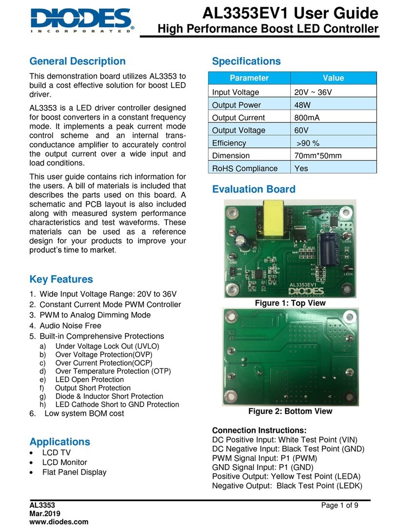
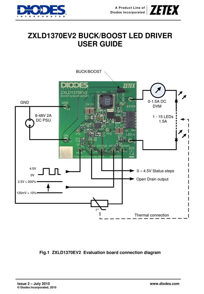
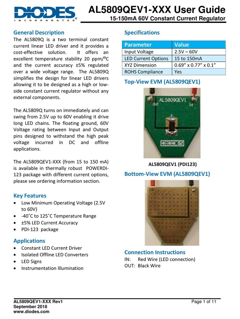
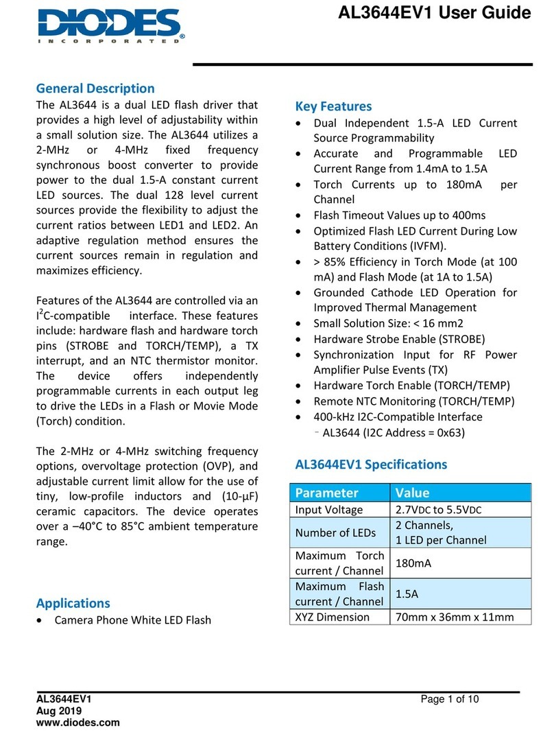
Diodes AP3917B User manual

Dual Output Off-Line Non-isolated Fly-back Power Solution
AP3917B 12V/20mA+3.8V20mA EV3 Board User’s Guide
AP3917B EV3 Page 1 of 17 06-21-2019
Rev 1.0 www.diodes.com
Table of Content
Chapter1 Induction.................................................2
1.1 General Description........................................2
1.2 AP3917B Key Features..................................2
1.3 Applications....................................................2
1.4 Board Picture..................................................2
Chapter2 Power Supply Specification..................3
2.1 system performance.......................................3
2.2 Environment...................................................3
Chapter3 Schematic and bill of material ..............4
3.1 Schematic.......................................................4
3.2 Bill of Material.................................................4
3.3 Transformer Specification ..............................5
3.3.1 Electrical Diagram...................................5
3.3.2 Transformer Instructions.........................5
3.3.3 Electrical Specifications..........................5
Chapter4 Evaluation Board Connections ............5
4.1 PCB Layout ....................................................5
4.2 Circuit Description..........................................6
4.2.1 Input EMI Filtering...................................6
4.2.2 Control IC................................................6
4.2.3 Flyback block..........................................6
4.2.4 Output Rectification ................................6
4.2.5 Output Feedback ....................................6
4.3 Quick Start Guide...........................................6
Chapter5. System test............................................7
5.1 Input & Output Characteristics.......................7
5.1.1 Input Standby Power ..............................7
5.1.2 Efficiency.................................................7
5.1.3 Line Regulation.......................................8
5.1.4 load regulation ........................................9
5.2 Key Performance test.....................................9
5.2.1 Start up performance..............................9
5.2.2 Voltage Stress.......................................10
5.2.3 Output Ripple & Noise ..........................11
5.2.4 Dynamic Response...............................12
5.3 Protection(SCP) test ....................................13
5.4 Thermal Test................................................14
5.5 System EMI Scan.........................................15
5.5.1 Conduction EMI test of 230V@full load15
5.5.2 Conduction EMI test of 110V@full load16

Dual Output Off-Line Non-isolated Fly-back Power Solution
AP3917B 12V/20mA+3.8V20mA EV3 Board User’s Guide
AP3917B EV3 Page 2 of 17 06-21-2019
Rev 1.0 www.diodes.com
Chapter1 Induction
1.1 General Description
AP3917B is an off-line universal AC Voltage input step-down regulator that provides accurate constant voltage (CV), outstanding
low standby power, light loading efficiency and dynamics performance. The chip supports non-isolated buck and buck-boost
topology, and also isolated and non-isolated flyback topology. The main applications are for cost-effective home appliance
power.
Working with a single winding inductor and integrating a 650V MOSFET when used in buck topology, the BOM cost is very low.
The AP3917B EV3 Evaluation Board contains two outputs specifications: 12V20mA and 3.8V20mA, with both non-isolations
flyback. The two outputs share a three-winding transformer. The feedback circuitry samples 3.8V output. The user’s guide
provides good design example for dual output power applications in home appliance power.
1.2 AP3917B Key Features
Universal 85V to 264V VAC Input
Internal MOSFET 650V (Rds(on) 10Ωmax. @25℃)
Maximum output Current: 170mA typ.@5V output
Low Standby Power Consumption
High Light Loading Efficiency and average efficiency can meet DOE IV and CoC V5 Tier
2
Frequency Modulation to suppress EMI to meet EN55032 and FCC part 15 class B
Rich Protection including: OTP, OLP, OLD,SCP
Extremely low system component count.
Totally Lead-free & Fully RoHS Compliant (SO-7)
Halogen and Antimony Free. “Green” Device
1.3 Applications
Non-Isolated Home Appliances including: AC Fans, Rice Cooker, Air conditioner, Coffee Machines, Soy Milk Machines, ect.
Auxiliary Power to IoT Devices.
1.4 Board Picture
Fig.1-1, Top View
Fig. 1-2, Bottom View

Dual Output Off-Line Non-isolated Fly-back Power Solution
AP3917B 12V/20mA+3.8V20mA EV3 Board User’s Guide
AP3917B EV3 Page 3 of 17 06-21-2019
Rev 1.0 www.diodes.com
Chapter2 Power Supply Specification
2.1 system performance
The system performance included in and output characters, specifications, EMC, protection, ect.
Items
Min.
Typ.
Max.
Comments
input characters
Input AC voltage rating
100V/60Hz
115/230
240V/50Hz
Two wire, no PE
Input AC voltage range
85V/60Hz
-
264V/50Hz
Input AC frequency range
47Hz
50/60
63Hz
Output characters
Output voltage 1
11.1V
12.0V
12.9V
Test at board terminal
Output voltage 1
3.61V
3.8V
3.99V
loading current 1
0
-
20mA
mA
loading current 2
4
-
20mA
performance specifications
Standby power
-
12mW
@230V/50Hz
Efficiency
-
74.32%/72.98%
-
@full load, 115V/230V
Ripple & Noise
12V
-
192mV
220mV
@full load
3.8V
-
101mV
150mV
Start up time
-
16.8ms
20ms
@full load, 85V/60Hz
EMC test
ESD test
Air
±15kV
-
-
@full load condition
contract
±8kV
-
-
Surge Test
±0.5kV
-
-
Differential mode, 2ohm,
1.2/50us
Conduction
EMI
110V
6dB margin
-
-
FCC Part 15 Class B
230V
6dB margin
-
-
EN55032
Protection function
SCP test
-
-
-
OK
OLP test
-
-
-
OK
OTP test
135℃
150℃
165℃
OK
2.2 Environment
Operation temperature: -20℃~85℃
Operation Humidity: 20%~90% R.H.
Storage temperature: 0~40℃
Storage Humidity: 0%~95% R.H.

Dual Output Off-Line Non-isolated Fly-back Power Solution
AP3917B 12V/20mA+3.8V20mA EV3 Board User’s Guide
AP3917B EV3 Page 4 of 17 06-21-2019
Rev 1.0 www.diodes.com
Chapter3 Schematic and bill of material
3.1 Schematic
Fig. 3-1, Evaluation Board Schematic
3.2 Bill of Material
Table 3-1, bill of material
Item
Designator
Description
Footprint
Qty.
Manufacturer
1
F1
8.2R, fusible resistor
Φ3*10mm
1
OAHE
2
BD1
ABS10A, bridge diode
SOPA-4
1
Diodes
3
C1
2.2uF/400V, electrolytic capacitor
Φ6*9mm
1
Aishi
4
C2
2.2uF/25V, X7R
SMD 0805
1
Telesky
5
C3
100uF/16V, electrolytic capacitor
Φ6*7mm
1
Aishi
6
C4
10uF/16V, X7R
SMD 0805
1
Telesky
7
C5
22uF/16V, electrolytic capacitor
Φ5*10mm
1
Telesky
8
C6
470pF/500V, X7R
SMD 0805
1
Telesky
9
C7
470pF/50V, X7R
SMD 0805
1
Telesky
10
D1
S1MWF-7, slow type diode, mark
F9
SOD123-FL
1
Diodes
11
D2
ES1J, 1A/600V, Trr 35ns
SMA
1
Diodes
12
D3
APD260, Schottky diode, 2A/60V
DO-41
1
Diodes
13
L1
2.2mH,choke inductor
DIP, 0406
1
Deloop
14
T1
EE8.3, Horizontal
DIP, 3+3Pin,
Horizontal
1
Deloop
15
R1
24.7k, thick film
SMD 0805, 1%
1
Panasonic
16
R2
13.0k, thick film
SMD 0805, 1%
1
Panasonic
17
R3
330k, thick film
SMD 0805, 5%
1
Panasonic
18
R4
27k, thick film
SMD 0805, 5%
1
Panasonic
19
U1
AP3917B
SO-7
1
Diodes
total
19pcs
R3
D1
C6
C7
BD1
F1
C1
C2
L1
L
T1
R1
R4
D2
N
U1
D3
C4C5
C3
Source
Source
VCC
Drain FB
12V-
/3.8V-
3.8V+
12V+
R2

Dual Output Off-Line Non-isolated Fly-back Power Solution
AP3917B 12V/20mA+3.8V20mA EV3 Board User’s Guide
AP3917B EV3 Page 5 of 17 06-21-2019
Rev 1.0 www.diodes.com
3.3 Transformer Specification
3.3.1 Electrical Diagram
Bobbin: EE8.3, 3+3Pin, Horizontal
Core: PC40, Ae=7mm2
Fig. 3-2, transformer electrical diagram
3.3.2 Transformer Instructions
Winding
Wire
Turns
Notes
5-6
0.11mm*1 UEW
123
three layer with tight tension
Tape
W=5mm
2
Full layer
3-4
0.17mm*2 UEW
10.5
One layer with tight tension
Tape
W=5mm
2
Full layer
1-3
0.17mm*1 UEW
23
One layer with tight tension
Tape
W=7mm
2
Full layer
Note: the transformer need be varnished. Put the transformer in the varnish for 30min, then remove it to the oven at 90℃for at
least 6 hours.
3.3.3 Electrical Specifications
Item
Pins
Inductance
Conditions
Main inductance
5-6
800uH±7%
1/3/4pin open, 1V/10kHz
Leak inductance
5-6
<50uH
1/3/4pin short, 1V/10kHz
Chapter4 Evaluation Board Connections
4.1 PCB Layout
6
4
5
3
WD1,
123Ts 0.11mm*1
WD2, 10.5Ts
0.17mm*2
1
WD3, 22Ts
0.17mm*1

Dual Output Off-Line Buck + Fly-back Power Solution
AP3917B 12V/20mA+3.8V20mA EV3 Board User’s Guide
AP3917 EV1 Draft 1.0 Page 6 of 17 www.diodes.com
Fig. 4-1, PCB Board Layout Top View
Fig. 4-2, PCB Board Layout Bottom View
4.2 Circuit Description
4.2.1 Input EMI Filtering
The input stage is composed of fusible resistor RF1, bridge diodes (BD1), Capacitors C1 and inductor L1. Resistor RF1 is a
flame proof, fusible, wire-wound resistor. It limits inrush current to safe levels for bridge diodes, provides differential mode noise
reduction and acts as an input fuse in the event of short circuit. Inductor L1 and Capacitor C1 constitute a LC filter, which can
smooth the input voltage and improve EMI conduction.
4.2.2 Control IC
AP3917B co-packages a 650V power MOSFET and control circuitry into a cost-effective SO-8 package. The device gets its
start-up current from DRAIN pin with a small capacitor C3 connect to BP pin when AC source is applied.
4.2.3 Flyback block
The flyback system which coupled in a transformer contains two output, 12V and 3.8V. The 3.8V output winding and 12V output
winding are in series, so if the turn ratio of 12V winding to 3.8V winding approximate to 12/3.8, the output voltage can be fixed to
12V and 3.8V.
4.2.4 Output Rectification
During the ON time of U1, current ramps in the main inductance of transformer T1 until the current reaches to the Ipk. During the
OFF time the inductor current ramps down via diodes D2 and D3. D2 andD3 must be ultra-fast diode or schottky diode (Trr<50ns
or lower). Capacitor C3/C5 should be selected to have an adequate ripple margin.
4.2.5 Output Feedback
The voltage across C4/C5 is quite smooth, so the divider R1 and R2 can reflect the output voltage. The output voltage dividend
by R1 and R2 was sent to feedback pin to regulate the 3.8V output voltage, thus regulate the 12V output voltage. A small
capacitor C7 about several hundreds of pF was used to prevent sharp noise of sampling circuit.
4.3 Quick Start Guide
1. The evaluation board is preset at 12V/20mA+3.8V20mA from output.
2. Ensure that the AC source is switched OFF or disconnected before doing connection.
3. Connect the AC line wires of power supply to “L and N” on the left side of the board.
4. Turn on the AC main switch.
5. Measure output terminals to ensure correct output voltages of Vo1 and Vo2 respectively.

Dual Output Off-Line Non-isolated Flyback Power Solution
AP3917B 12V/20mA+3.8V20mA EV3 Board User’s Guide
AP3917B EV3 Page 7 of 17 06-21-2019
Rev 1.0 www.diodes.com
Chapter5. System test
5.1 Input & Output Characteristics
5.1.1 Input Standby Power
The standby power and output voltage was tested after 10min burning. The voltage data was tested at the PCB terminal. All the
data was tested at room temperature.
Table 5-1, standby power and no load output voltage
Input Voltage
Pin (mW)
Vo1 (V)
Vo2 (V)
85V/60Hz
5.0
3.791
12.202
115V/60Hz
5.4
3.791
12.205
230V/50Hz
7.8
3.788
12.197
264V/50Hz
8.6
3.788
12.197
Fig. 5-1, Standby Power versus Vin Curve
5.1.2 Efficiency
The efficiency data was tested after 10min burning, and it was tested at the PCB terminal. All the data was tested at room
temperature. 12V and 3.8V full load, input voltage range from 85V/60Hz to 265V/50Hz.
Table 5-2, Full load efficiency VS Vin data
Vin
Vo1(V)
Vo2(V)
Pin(W)
Eff.
85V/60Hz
3.752
12.291
0.451
73.22%
115V/60Hz
3.746
12.280
0.452
72.98%
150V/60Hz
3.749
12.282
0.444
74.32%
180V/50Hz
3.748
12.280
0.446
73.97%
200V/50Hz
3.748
12.280
0.447
73.80%
230V/50Hz
3.746
12.280
0.452
72.98%
265V/50Hz
3.746
12.278
0.460
71.70%
0
2
4
6
8
10
12
80 100 120 140 160 180 200 220 240 260 280
Pin(mW)
Vin (V)
Standby Power

Dual Output Off-Line Non-isolated Flyback Power Solution
AP3917B 12V/20mA+3.8V20mA EV3 Board User’s Guide
AP3917B EV3 Page 8 of 17 06-21-2019
Rev 1.0 www.diodes.com
Fig. 5-2, Full load efficiency VS Vin
5.1.3 Line Regulation
The line regulation data was tested after 10min burning. The voltage data was tested at the PCB terminal. All the data was
tested at room temperature. 3.8V and 12V full load, Vin ranges from 85V to 264V.
Table 5-3, line and load regulation data
Vin
Vo1 output(V)
Vo2 output(V)
Vin
Vo1(V)
Vo2(V)
85V/60Hz
3.752
12.291
115V/60Hz
3.746
12.280
150V/60Hz
3.749
12.282
180V/50Hz
3.748
12.280
200V/50Hz
3.748
12.280
230V/50Hz
3.746
12.280
265V/50Hz
3.746
12.278
Fig 5-3, 3.8V and 12V full load, output voltage versus input voltag
60.00%
64.00%
68.00%
72.00%
76.00%
80.00%
80 100 120 140 160 180 200 220 240 260 280
Efficiency
Vin(V)
Full load efficiency VS Vin
0
2
4
6
8
10
12
14
80 100 120 140 160 180 200 220 240 260 280
Output Voltage(V)
Vin(V)
Full Load Output Voltage VS Vin
3.8V
12V

Dual Output Off-Line Non-isolated Flyback Power Solution
AP3917B 12V/20mA+3.8V20mA EV3 Board User’s Guide
AP3917B EV3 Page 9 of 17 06-21-2019
Rev 1.0 www.diodes.com
5.1.4 Load Regulation
The load regulation data was tested after 10min burning. The voltage data was tested at the PCB terminal. All the data was
tested at room temperature. The load of Vo1 and Vo2 terminals both ranges from 10% to 100%.
Table 5-4, Vo1 and Vo2 output voltage
Vin
10%
25%
50%
75%
100%
Vo1(V)
Vo2(V)
Vo1(V)
Vo2(V)
Vo1(V)
Vo2(V)
Vo1(V)
Vo2(V)
Vo1(V)
Vo2(V)
85V/60Hz
3.788
11.578
3.785
11.772
3.788
11.937
3.772
12.057
3.768
12.157
115V/60Hz
3.788
11.585
3.784
3.777
3.774
11.932
3.772
12.052
3.766
12.157
230V/50Hz
3.786
11.572
3.781
11.757
3.774
11.922
3.769
12.047
3.764
12.147
265V/50Hz
3.785
11.572
3.780
11.755
3.774
11.922
3.768
12.045
3.763
12.147
Fig. 5-4, 12V and 5V output voltage@ 3.8V no load
5.2 Key Performance test
5.2.1 Start up performance
The start-up time was measured with differential probe clipping on the input AC source, and the common low-voltage probe
clipping on the output terminal. Before start-up, the buck cap should be discharged.
Table 5-5, start up performance
Input voltage
Start up time
figures
85V/60Hz
16.8ms
Fig. 15
115V/50Hz
16.1ms
Fig. 16
230V/50Hz
15.3ms
Fig. 17
264V/60Hz
14.6ms
Fig. 18
0
1
2
3
4
5
6
7
8
9
10
11
12
13
80 100 120 140 160 180 200 220 240 260 280
Output Voltage(V)
Vin(V)
Load Regulation
Vo1-85V/60Hz
Vo1-115V/60Hz
Vo1-230V/50Hz
Vo1-265V/50Hz
Vo2-85V/60Hz
Vo2-115V/50Hz
Vo2-230V/50Hz
Vo2-265V/50Hz

Dual Output Off-Line Non-isolated Flyback Power Solution
AP3917B 12V/20mA+3.8V20mA EV3 Board User’s Guide
AP3917B EV3 Page 10 of 17 06-21-2019
Rev 1.0 www.diodes.com
Turn on Waveforms
CH1: Vin; CH2: 3.8V output; CH3:12V output
Fig. 5-5, Start up time is 16.8ms @full load, 85V/60Hz
Fig 5-6, Start up time is 16.1ms @full load, 115V/60Hz
Fig. 5-7, Start up time is 15.3ms @full load, 230V/50Hz
Fig 5-8, Start up time is 14.6ms @full load, 265V/50Hz
5.2.2 Voltage Stress
The voltage tested below was between the source and the drain pin of IC. The test need use differential probe. The Vak voltage
is tested between the anode and cathode of flyback diode D2/D3.
Table 5-6, MOSFET drain-source and flyback diodes Vak voltage stress
Input voltage
Voltage stress
figures
Vds(V)
Vak1(V)
Vak2(V)
85V/60Hz
221
17
57
Fig. 19
115V/50Hz
265
21
65
-
230V/50Hz
429
37
119
-
264V/60Hz
484
42
129
Fig. 22

Dual Output Off-Line Non-isolated Flyback Power Solution
AP3917B 12V/20mA+3.8V20mA EV3 Board User’s Guide
AP3917B EV3 Page 11 of 17 06-21-2019
Rev 1.0 www.diodes.com
CH1: Vds/Vak2; CH2: Vak1
Fig. 5-9, MOS drain-source 221V@85V/60Hz, full load
Fig. 5-10, Vo1 terminal Vak 17V, Vo2 Vak 57V@85V/60Hz, full
load
Fig. 5-11, MOS drain-source 484V @265V/50Hz, full load
Fig. 5-12,Vo1 terminal Vak 129V, Vo2 Vak 42V@264V/50Hz,full
load
5.2.3 Output Ripple & Noise
The ripple and noise was tested at PCB terminal, using coaxial cable (1:1). The bandwidth was limited to 20MHz. A 10uF
electrolytic capacitor and a 104 ceramic capacitor should be paralleled to the output terminal.
Table 5-7, ripple & noise
Conditions
Input voltage
R&N(mV)
Figures
Vo1 terminal
Vo2 terminal
3.8V full load, 12V full load
85V/60Hz
96
184
Fig. 23
115V/50Hz
96
184
-
230V/50Hz
101
192
-
264V/60Hz
101
190
Fig. 24
CH1:Vo1 output; CH4:Vo2 output

Dual Output Off-Line Non-isolated Flyback Power Solution
AP3917B 12V/20mA+3.8V20mA EV3 Board User’s Guide
AP3917B EV3 Page 12 of 17 06-21-2019
Rev 1.0 www.diodes.com
Fig.5-13, Output R&N 96/184[email protected]and 12V full load, 85V/60Hz
115V/60Hz
230V/50Hz
265V/50Hz
5.2.4 Dynamic Response
The dynamic response output voltage was tested at the PCB terminal, and the bandwidth was limited to 20MHz. The loading is
set 0mA as low load and 20mA as high load, and last for 0.1s respectively. The ramp is set at 40mA/us.
Table 5-8, dynamic response
Conditions
Vin
Output voltage(V)
Figures
Vo1
Vo2
Max (V)
Min (V)
Max (V)
Min (V)
12V full load,
3.8V loading
0~100%
85V/60Hz
4.16
3.62
12.94
8.65
Fig. 27
115V/60Hz
4.10
3.65
12.87
8.52
-
230V/50Hz
4.06
3.65
12.87
8.71
-
264V/50Hz
4.10
3.65
12.94
8.31
Fig. 28
3.8V full load,
12V loading
0~100%
85V/60Hz
3.98
3.63
15.01
12.00
Fig. 29
115V/60Hz
3.95
3.63
15.01
11.94
-
230V/50Hz
4.02
3.63
15.01
11.94
-
264V/50Hz
4.02
3.63
15.07
11.94
Fig. 30

Dual Output Off-Line Non-isolated Flyback Power Solution
AP3917B 12V/20mA+3.8V20mA EV3 Board User’s Guide
AP3917B EV3 Page 13 of 17 06-21-2019
Rev 1.0 www.diodes.com
CH3:12V output; CH2:3.8V output
Fig. 5-18 dynamic response@3.8V 0~20mA,12V FL, @265V/50Hz
Fig.5-19, dynamic response@12V 0~20mA,3.8V FL, @85V/60Hz
Fig. 5-20, dynamic response@12V 0~20mA,3.8V FL, @265V/50Hz
5.3 Protection (SCP) test
The SCP test was measured under the condition of output cable terminal short circuit.
Table 5-9, the short circuit protection test
Condition
Vin
Vo1 max(V)
Vo2 max(V)
Figures
12V terminal output short
85V/60Hz
0.416
0.508
Fig. 31
115V/60Hz
0.425
0.512
-
230V/50Hz
0.463
0.503
-
264V/50Hz
0.480
0.508
Fig. 32
3.8V terminal output short
85V/60Hz
0.544
2.81
Fig. 33
115V/60Hz
0.562
2.90
-
230V/50Hz
0.588
3.05
-
264V/50Hz
0.608
3.07
Fig. 34
CH2:3.8V output; CH3:12V output

Dual Output Off-Line Non-isolated Flyback Power Solution
AP3917B 12V/20mA+3.8V20mA EV3 Board User’s Guide
AP3917B EV3 Page 14 of 17 06-21-2019
Rev 1.0 www.diodes.com
Fig. 5-21, SCP @12V output short and 3.8V full load, 85V/60Hz
Fig. 5-22, SCP @12V output short and 3.8V full load, 265V/50Hz
Fig. 5-23, SCP@12V output short and 3.8V full load, 85V/60Hz
Fig. 5-24, SCP@12V output short and 3.8V full load, 265V/50Hz
5.4 Thermal Test
The thermal test was under room temperature after burning 1 hour. The board has no case, and using thermal imager to observe
the surface temperature of IC.
Fig. 5-25, IC 32.1℃, 12V flyback diode 31.9℃, RCD diode
33.1℃@full load, 85V/60Hz, ambient temperature 26.9℃.
Fig. 5-26, Transformer 33.3℃, 3.8V flyback diode 31.7℃@full
load, 264V/50Hz, ambient temperature 25.8℃.

Dual Output Off-Line Non-isolated Flyback Power Solution
AP3917B 12V/20mA+3.8V20mA EV3 Board User’s Guide
AP3917B EV3 Page 15 of 17 06-21-2019
Rev 1.0 www.diodes.com
Fig. 5-27, IC 34.5℃, 12V flyback diode 31.5℃, RCD diode
31.9℃@full load, 265V/50Hz, ambient temperature 26.3℃.
Fig. 5-28, Transformer 33.5℃, 3.8V flyback diode 31.8℃@full
load, 264V/50Hz, ambient temperature 25.4℃.
5.5 System EMI Scan
The power supply passed EN55022 Class B (for 230V input) and FCC part 15 (for 110V input) EMI requirement with more than
6dB margin.
5.5.1 Conduction EMI test of 230V@full load
The test result can pass EN55022 Class B limitation with more than 6dB margin.
Fig. 5-29, L line conduction waveform@230V, full load.
Fig. 5-30, L line conduction data@230V, full load.

Dual Output Off-Line Non-isolated Flyback Power Solution
AP3917B 12V/20mA+3.8V20mA EV3 Board User’s Guide
AP3917B EV3 Page 16 of 17 06-21-2019
Rev 1.0 www.diodes.com
Fig. 5-31, N line conduction waveform@230V, full load.
Fig. 5-32, N line conduction data@230V, full load.
5.5.2 Conduction EMI test of 110V@full load
The test result can pass FCC part 15 limitation with more than 6dB margin.
Fig. 5-33, L line conduction waveform@110V, full load.
Fig. 5-34, L line conduction data@110V, full load.
Fig. 5-35, N line conduction waveform@110V, full load.
Fig. 5-36, N line conduction data@110V, full load.

Dual Output Off-Line Non-isolated Flyback Power Solution
AP3917B 12V/20mA+3.8V20mA EV3 Board User’s Guide
AP3917B EV3 Page 17 of 17 06-21-2019
Rev 1.0 www.diodes.com
IMPORTANT NOTICE
DIODES INCORPORATED MAKES NO WARRANTY OF ANY KIND, EXPRESS OR IMPLIED, WITH REGARDS
TO THIS DOCUMENT, INCLUDING, BUT NOT LIMITED TO, THE IMPLIED WARRANTIES OF
MERCHANTABILITY AND FITNESS FOR A PARTICULAR PURPOSE (AND THEIR EQUIVALENTS UNDER THE
LAWS OF ANY JURISDICTION).
Diodes Incorporated and its subsidiaries reserve the right to make modifications, enhancements, improvements, corrections or
other changes without further notice to this document and any product described herein. Diodes Incorporated does not assume
any liability arising out of the application or use of this document or any product described herein; neither does Diodes
Incorporated convey any license under its patent or trademark rights, nor the rights of others. Any Customer or user of this
document or products described herein in such applications shall assume all risks of such use and will agree to hold Diodes
Incorporated and all the companies whose products are represented on Diodes Incorporated website, harmless against all
damages.
Diodes Incorporated does not warrant or accept any liability whatsoever in respect of any products purchased through
unauthorized sales channel.
Should Customers purchase or use Diodes Incorporated products for any unintended or unauthorized application, Customers
shall indemnify and hold Diodes Incorporated and its representatives harmless against all claims, damages, expenses, and
attorney fees arising out of, directly or indirectly, any claim of personal injury or death associated with such unintended or
unauthorized application.
Products described herein may be covered by one or more United States, international or foreign patents pending. Product
names and markings noted herein may also be covered by one or more United States, international or foreign trademarks.
This document is written in English but may be translated into multiple languages for reference. Only the English version of this
document is the final and determinative format released by Diodes Incorporated.
LIFE SUPPORT
Diodes Incorporated products are specifically not authorized for use as critical components in life support devices or systems
without the express written approval of the Chief Executive Officer of Diodes Incorporated. As used herein:
A. Life support devices or systems are devices or systems which:
1. are intended to implant into the body, or
2. support or sustain life and whose failure to perform when properly used in accordance with instructions for
use provided in the labeling can be reasonably expected to result in significant injury to the user.
B. A critical component is any component in a life support device or system whose failure to perform can be reasonably
expected to cause the failure of the life support device or to affect its safety or effectiveness.
Customers represent that they have all necessary expertise in the safety and regulatory ramifications of their life support devices
or systems, and acknowledge and agree that they are solely responsible for all legal, regulatory and safety-related requirements
concerning their products and any use of Diodes Incorporated products in such safety-critical, life support devices or systems,
notwithstanding any devices- or systems-related information or support that may be provided by Diodes Incorporated. Further,
Customers must fully indemnify Diodes Incorporated and its representatives against any damages arising out of the use of
Diodes Incorporated products in such safety-critical, life support devices or systems.
Copyright © 2016, Diodes Incorporated
www.diodes.com
Table of contents
Other Diodes Controllers manuals
Popular Controllers manuals by other brands
Siemens
Siemens SINAMICS V90 operating instructions

Dräger
Dräger REGARD-1 Instructions for use
Franke
Franke AQUA802 Installation and operating instructions
Plecter Labs
Plecter Labs Crystal Focus Saber Core V10.0 user manual
NDS
NDS Dometic EM12-150 Installation and operating manual
TIME LED
TIME LED 781296 Installation and operating instructions
Plasmatronics
Plasmatronics DINGO D8040N user guide
Rockwell Automation
Rockwell Automation Allen-Bradley MicroLogix 1400 user manual
Eaton
Eaton SVX9000 Series manual
Savant
Savant CPT-1212 Quick reference guide
Eaton
Eaton COOPER POWER SERIES Installation and operation instructions
Hach
Hach AS950 AWRS Basic operations
