Diodes PI5USB31213AXEA User manual

ORIGINATE DATE
16 May, 2017
EDIT DATE
20 July, 2017 DOCUMENT-REV 1.1 PAGE
Page 1 of 14
AE Format Rev 1.2
Diodes Incorporated (Milpitas office)
1545 Barber Lane, Milpitas, CA 95035 U.S.A.
PI5USB31213AXEA Demo Board Rev.B User Manual
Table of Contents
1 Introduction .................................................................................................................................. 2
2 Overview ....................................................................................................................................... 2
3 Quick Start .................................................................................................................................... 4
3.1 Source(DFP) Mode ................................................................................................................... 4
3.2 Battery-powered Sink(UFP) Mode ........................................................................................... 5
3.3 Bus-powered Sink(UFP) Mode ................................................................................................ 6
3.4 Try.SNK DRP Mode .................................................................................................................. 7
4 Circuit Description ....................................................................................................................... 9
4.1 DIP Switch Setting .................................................................................................................... 9
4.2 Mode Selection, I2C Address and I2C Bus ............................................................................ 9
4.3 VBUS Power Supply ................................................................................................................. 9
4.4 Power ...................................................................................................................................... 10
4.5 Disable/Low Power State ....................................................................................................... 10
5 Appendix A: Demo Board Schematic....................................................................................... 12
6 Appendix B: Demo Board Picture ............................................................................................ 13
ORIGINATE DATE
16 May, 2017
EDIT DATE
20 July, 2017 DOCUMENT-REV 1.1 PAGE
Page 2 of 14
AE Format Rev 1.2
Diodes Incorporated (Milpitas office)
1545 Barber Lane, Milpitas, CA 95035 U.S.A.
1 Introduction
PI5USB31213A is a dual differential channel bi-directional Mux/Demux switch with plug-in detector for USB 3.1
Type-C connector applications.
PI5USB31213A is designed for USB 3.1 Gen2 (10 Gbps) application.
The device includes:
1) The Plug-in Detector for Type-C connector (CC Sensing)
a) Supports Source/Sink/DRP/Try.SRC DRP/Try.SNK DRP
2) Integrated 2:1 USB3.0 Mux/DeMux
a) Auto-configure ports orientation through CC Sensing
3) Integrated VCONN switch to power active cable
PI5USB31213A detects the plug-in orientation of the cable at a Type-C connector and switches between the USB
controller and the new Type-C connector. It supports Host(Source/DFP) mode, Device(Sink/UFP) mode, Dual Role
Port(DRP), Try.SRC DRP and Try.SNK DRP with automatic configuration based on the voltage levels detected on CC
pins. It offers excellent signal integrity for high-speed signals at low power dissipation. PI5USB31213A enters disabled
state when ENB pin is pulled up to VDD through an internal resistor.
PI5USB31213A supports both pin and I2C control base on ADDR pin setting. It allows the system choose between pin
control and I2C control mode. In pin control mode, the PORT input pin determines the port setting in which Source(DFP)
only mode, Sink(UFP) only mode or Try.SNK DRP can be selected. Enabling I2C control mode allows higher flexibility for
port control and communications through registers read/write in PI5USB31213A. There is also flexibility to support Default,
1.5A and 3A current modes. An interrupt signal for indicating changes with the I2C registers is sent to the master to notify
the system any change in the Type-C connector while in parallel the system can still monitor ID pin.
This user manual describes the components and the usage of PI5USB31213A Demo Board Rev.B.
2 Overview
Figure 1 is the block diagram of Diodes PI5USB31213A demo board and figure 2 shows the demo board layout. A USB-C
cable can be connected between the USB-C receptacle connector (J1) on PI5USB31213A demo board and another USB-
C device. A USB-C to USB-A cable can be connected between J1 and a USB host, such as PC. A USB-C to USB-A
receptacle adapter can be connected between J1 and a USB device, such as USB flash drive. One USB3 micro-AB
receptacle (J2) is used to connect mobile phones/notebook/tablet/PC to transmit USB3 data to/from J1.
Slide switch at reference SW1 is used to set control mode (GPIO/I2C) and operating mode (Source/Sink/DRP) of
PI5USB31213A and LED indicator to SDA/SCL/INTB/ID pins of PI5USB31213A. The processor can connect to
SDA/SCL/INTB/ID pins through pin header JP18/JP17/JP15 or Test Header J3.
+5V can be employed to the demo board via 5VPW header pin or mini-B receptacle (J4).
VBUS of Type-C connector can be source from on-board VBUS switch via JP4.

ORIGINATE DATE
16 May, 2017
EDIT DATE
20 July, 2017 DOCUMENT-REV 1.1 PAGE
Page 3 of 14
AE Format Rev 1.2
Diodes Incorporated (Milpitas office)
1545 Barber Lane, Milpitas, CA 95035 U.S.A.
Figure 1: Simplified Block Diagram of PI5USB31213A Demo Board Rev.B
Figure 2: Layout of PI5USB31213A Demo Board Rev.B
ORIGINATE DATE
16 May, 2017
EDIT DATE
20 July, 2017 DOCUMENT-REV 1.1 PAGE
Page 4 of 14
AE Format Rev 1.2
Diodes Incorporated (Milpitas office)
1545 Barber Lane, Milpitas, CA 95035 U.S.A.
3 Quick Start
This section provides different configuration examples to start-up PI5USB31213A demo board rev.B in Source, Sink or DRP
mode.
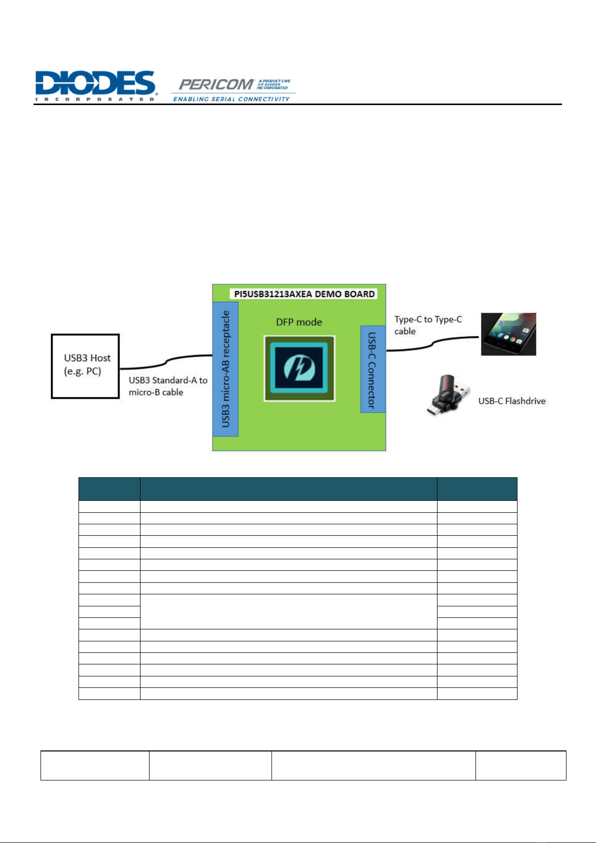
3.1 Source(DFP) Mode
To start-up the PI5USB31213A demo board rev.B in pin control DFP mode, complete the following steps:
1. Configure pin headers and DIP switches SW1 as shown in Table 1.
2. Power-up PI5USB31213A demo board by connecting J2 to a USB host using Type-A to micro-B cable. D2 should light
up indicating the board has power.
3. Connect PI5USB31213A demo board to a Type-C Sink(UFP) using a Type-C cable. D6 should light up indicating ID
pin is pulled low and 5V VBUS is provided by the demo board.
.
Figure 3: PI5USB31213A Demo Board DFP mode illustration.
Header pin/
Switch
Pin name/
Function
Setting
SW1.1 ENB = L ON
SW1.2 SCL/OUT2 LED indicator OFF
SW1.3 SDA/OUT1 LED indicator OFF
SW1.4 ADDR OFF
SW1.5 INTB/OUT3 LED indicator ON
SW1.6 ID LED indicator ON
SW1.7 PORT = H ON
SW1.8 PORT = L OFF
JP2
Enable On-board VBUS switch
ON
SW_EN ON
DISC2 ON
JP3 Demo board power by VBUSA ON
JP4 Connect output of VBUS switch to VBUSC ON
JP6 Connect VBUSC to VBUSA OFF
JP8 Connect VCONN to 5VPW ON
JP9 Connect 5VPW to VDD OFF
JP10 Enable 3.3V VDD ON
Table 1: PI5USB31213A Demo Board Rev.B DFP mode configuration.

ORIGINATE DATE
16 May, 2017
EDIT DATE
20 July, 2017 DOCUMENT-REV 1.1 PAGE
Page 5 of 14
AE Format Rev 1.2
Diodes Incorporated (Milpitas office)
1545 Barber Lane, Milpitas, CA 95035 U.S.A.
3.2 Battery-powered Sink(UFP) Mode
To start-up the PI5USB31213A demo board rev.B in pin control battery-powered UFP mode, complete the following steps:
1. Configure pin headers and DIP switches SW1 as shown in Table 2.
2. Connect J2 to a USB device using micro-A to Type-A receptacle.
3. Power up PI5UB31213A demo board by connecting J4 to a USB host using Type-A to mini-B cable (or connect +5V to
5VPW pin header). D2 should light up indicating the board has power.
4. Connect PI5USB31213A demo board to a Type-C Source(DFP) using a Type-C cable. 5V VBUS should be provided
by the Type-C Host/Source/DFP. D3 and D4 might light up depends on the DFP’s Type-C current mode setting.
Figure 4: PI5USB31213A Demo Board battery-powered UFP mode illustration.
Header pin/
Switch
Pin name/
Function
Setting
SW1.1 ENB = L ON
SW1.2 SCL/OUT2 LED indicator ON
SW1.3 SDA/OUT1 LED indicator ON
SW1.4 ADDR OFF
SW1.5 INTB/OUT3 LED indicator OFF
SW1.6 ID LED indicator OFF
SW1.7 PORT = H OFF
SW1.8 PORT = L ON
JP2
Enable On-board VBUS switch
OFF
SW_EN
OFF
DISC2 OFF
JP3 Demo board power by VBUSA OFF
JP4
Connect output of VBUS switch to VBUSC
OFF
JP6 Connect VBUSC to VBUSA ON
JP8 Connect VCONN to 5VPW OFF
JP9
Connect 5VPW to VDD
OFF
JP10 Enable 3.3V VDD ON
Table 2: PI5USB31213A Demo Board Rev.B battery-powered UFP mode configuration.

ORIGINATE DATE
16 May, 2017
EDIT DATE
20 July, 2017 DOCUMENT-REV 1.1 PAGE
Page 6 of 14
AE Format Rev 1.2
Diodes Incorporated (Milpitas office)
1545 Barber Lane, Milpitas, CA 95035 U.S.A.
3.3 Bus-powered Sink(UFP) Mode
To start-up the PI5USB31213A demo board rev.B in pin control VBUS-powered UFP mode, complete the following steps:
1. Configure pin headers and DIP switches SW1 as shown in Table 3.
2. Connect J2 to a USB device using micro-A to Type-A receptacle.
3. Connect PI5USB31213A demo board to a Type-C Source(DFP) using a Type-C cable. 5V VBUS should be provided
by the Type-C Host/Source/DFP. D2, D3 and D4 might light up depends on the DFP’s Type-C current mode setting.
Figure 5: PI5USB31213A Demo Board VBUS-powered UFP mode illustration.
Header pin/
Switch
Pin name/
Function
Setting
SW1.1 ENB = L ON
SW1.2
SCL/OUT2 LED indicator
ON
SW1.3 SDA/OUT1 LED indicator ON
SW1.4 ADDR OFF
SW1.5
INTB/OUT3 LED indicator
OFF
SW1.6 ID LED indicator OFF
SW1.7 PORT = H OFF
SW1.8
PORT = L
ON
JP2
Enable On-board VBUS switch
OFF
SW_EN OFF
DISC2
OFF
JP3 Demo board power by VBUSA ON
JP4 Connect output of VBUS switch to VBUSC OFF
JP6 Connect VBUSC to VBUSA ON
JP8 Connect VCONN to 5VPW OFF
JP9 Connect 5VPW to VDD OFF
JP10 Enable 3.3V VDD ON
Table 3: PI5USB31213A Demo Board Rev.B VBUS-powered UFP mode configuration.

ORIGINATE DATE
16 May, 2017
EDIT DATE
20 July, 2017 DOCUMENT-REV 1.1 PAGE
Page 7 of 14
AE Format Rev 1.2
Diodes Incorporated (Milpitas office)
1545 Barber Lane, Milpitas, CA 95035 U.S.A.
3.4 Try.SNK DRP Mode
To start-up the PI5USB31213A demo board rev.B in pin control Try.SNK DRP mode, complete the following steps:
1. Configure pin headers and DIP switches SW1 as shown in Table 3 in the next page.
2. Power up PI5UB31213A demo board by connecting J4 to a USB host using Type-A to mini-B cable. D2 should light up
indicating the board has power.
3. Connect PI5USB31213A demo board to a Type-C Sink(UFP) using a Type-C cable. D6 should light up indicating ID
pin is pulled low and 5V VBUS is provided by the demo board.
4. Connect PI5USB31213A demo board to a Type-C Source(DFP) using a Type-C cable. 5V VBUS should be provided
by the Type-C Host/Source/DFP. D3 and D4 might light up depends on the DFP’s Type-C current mode setting
5. Connect PI5USB31213A demo board to a Type-C DRP using a Type-C cable. PI5USB31213A should connect as
Sink/UFP due to Try.SNK feature. 5V VBUS should be provided by the port partner. D3 and D4 might light up depends
on port partner’s Type-C current mode setting.
6. Connect PI5USB31213A demo board to a Type-C Try.SNK DRP using a Type-C cable. PI5USB31213A may result in
either DFP or UFP mode. The result is random.
a. When connect as a Source/DFP/Host, D6 should light up indicating ID pin is pulled low and 5V VBUS is provided
by the demo board.
b. When connect as a Sink/UFP/Device. 5V VBUS should be provided by the port partner. D3 and D4 might light up
depends on port partner’s Type-C current mode setting.
Figure 6: PI5USB31213A Demo Board Try.SNK DRP mode illustration.
ORIGINATE DATE
16 May, 2017
EDIT DATE
20 July, 2017 DOCUMENT-REV 1.1 PAGE
Page 8 of 14
AE Format Rev 1.2
Diodes Incorporated (Milpitas office)
1545 Barber Lane, Milpitas, CA 95035 U.S.A.
Header pin/
Switch
Pin name/
Function
Setting
SW1.1 ENB = L ON
SW1.2 SCL/OUT2 LED indicator ON
SW1.3 SDA/OUT1 LED indicator ON
SW1.4 ADDR OFF
SW1.5 INTB/OUT3 LED indicator ON
SW1.6 ID LED indicator ON
SW1.7 PORT = H OFF
SW1.8 PORT = L OFF
JP2
Enable On-board VBUS switch
ON
SW_EN ON
DISC2 ON
JP3 Demo board power by VBUSA OFF
JP4 Connect output of VBUS switch to VBUSC ON
JP6 Connect VBUSC to VBUSA OFF
JP8 Connect VCONN to 5VPW ON
JP9 Connect 5VPW to VDD OFF
JP10 Enable 3.3V VDD ON
Table 4: PI5USB31213A Demo Board Rev.B Try.SNK DRP mode (pin control mode) configuration.

ORIGINATE DATE
16 May, 2017
EDIT DATE
20 July, 2017 DOCUMENT-REV 1.1 PAGE
Page 9 of 14
AE Format Rev 1.2
Diodes Incorporated (Milpitas office)
1545 Barber Lane, Milpitas, CA 95035 U.S.A.
4 Circuit Description
4.1 DIP Switch Setting
The DIP switch (SW1) is used to configure PI5USB31213A in different mode.
Header pin/
Switch
Pin name/
Function
Description
SW1.1 ENB ENB = Low if SW1.1 is ON.
ENB = High if SW1.1 is OFF.
SW1.2 SCL/OUT2 LED indicator For pin control mode:
OUT2 is connected to LED if SW1.2 is ON
For I2C mode:
SW1.2 shall be OFF.
SW1.3 SDA/OUT1 LED indicator For pin control mode:
OUT1 is connected to LED if SW1.3 is ON
For I2C mode:
SW1.2 shall be OFF.
SW1.4 ADDR For pin control mode: SW1.4 is OFF.
For I2C mode: SW1.4 is ON.
I2C mode; 0x0D (Default)
I2C mode; 0x2D (Remove R30 and solder R28)
SW1.5 INTB/OUT3 LED indicator OUT3 is connected to LED if SW1.5 is ON
SW1.6 ID LED indicator ID is connected to LED if SW1.6 is ON
SW1.7 PORT = H PORT = Open if SW1.7 is OFF
PORT = High if SW1.7 is ON
SW1.8 PORT = L PORT = Open if SW1.8 is OFF
PORT = Low if SW1.8 is ON
Table 5: DIP Switch SW1 settings
4.2 Mode Selection, I2C Address and I2C Bus
PI5USB31213A can be controlled via either GPIO or I2C mode. The control mode and I2C address is configured via ADDR
pin (refer to section 4.1). Pins 1 and 24 of PI5USB31213A are used for transmitting I2C SCL and SDA, respectively.
External pull-ups may be required for SCL(OUT2) and SDA(OUT1) pins when reading/writing I2C. Alternatively, pull-ups for
SCL(OUT2) and SDA(OUT1) can be enabled by short pins 1-2 and 3-4 of JP18.
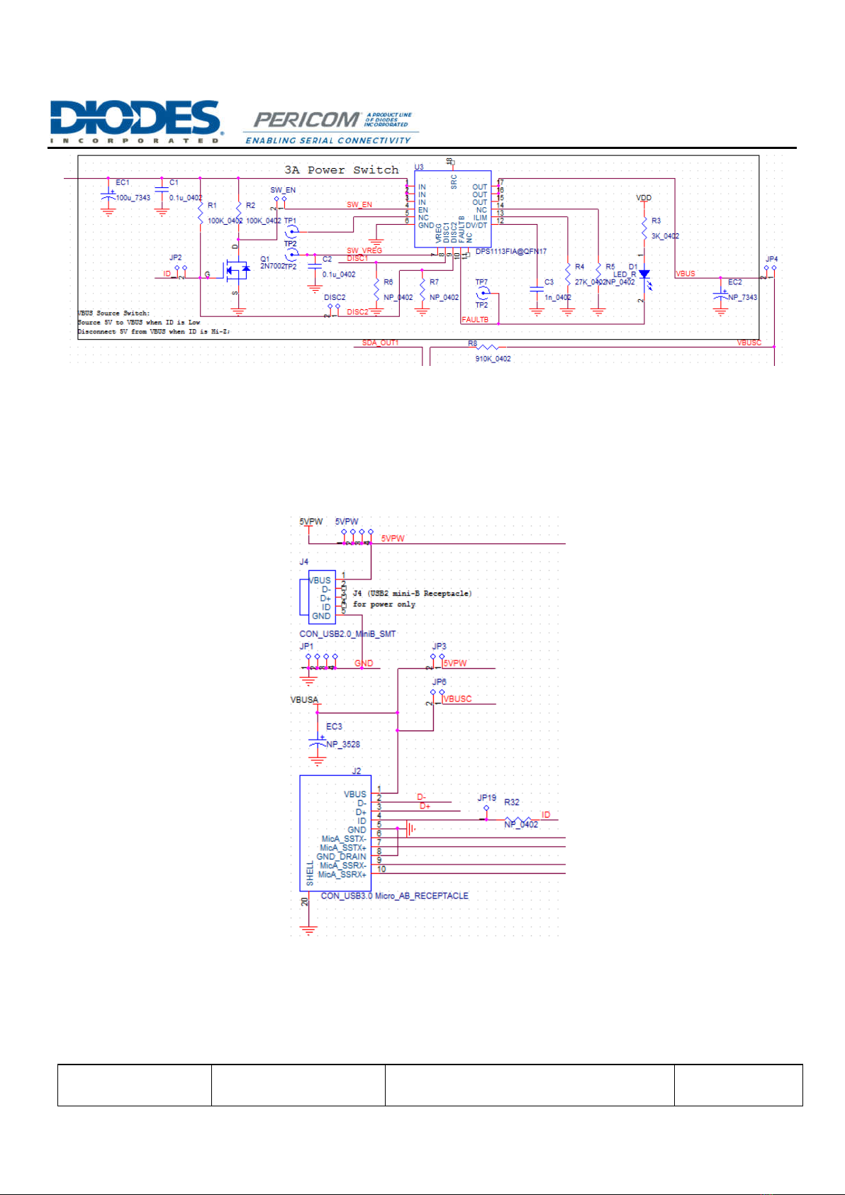
4.3 VBUS Power Supply
The system should drive 5V to VBUS of USB-C receptacle connector (J1) when a sink/UFP is attached. If an external
VBUS switch not available, a discrete VBUS switch DPS1113 is assembled on EVB, which is controlled by ID pin of
PI5USB31213A. This switch will turn on and drive VBUS, when a sink/UFP is attached. To use the on-board VBUS switch,
please shorts JP2, jumper SW_EN, jumper DISC2 and jumper JP4.
For detailed DPS1113 function and setting, please refer to DPS1113 datasheet.
ORIGINATE DATE
16 May, 2017
EDIT DATE
20 July, 2017 DOCUMENT-REV 1.1 PAGE
Page 10 of 14
AE Format Rev 1.2
Diodes Incorporated (Milpitas office)
1545 Barber Lane, Milpitas, CA 95035 U.S.A.
Figure 7: VBUS switch of PI5USB31213A Demo Board Rev.B
4.4 Power
In DRP and battery-powered UFP mode, the demo board can be powered by +5V VBUS through mini-B connector J4 or by
+5V through pin header 5VPW.
In DFP mode, the system/host can provide +5V through the USB micro-AB connector J2 to power up the board via JP3.
Figure 8: Power Supply option of PI5USB31213A Demo Board Rev.B
4.5 Disable/Low Power State
PI5USB31213A can be disabled by setting ENB pin to a high voltage level. Please refer section 4.1.

ORIGINATE DATE
16 May, 2017
EDIT DATE
20 July, 2017 DOCUMENT-REV 1.1 PAGE
Page 11 of 14
AE Format Rev 1.2
Diodes Incorporated (Milpitas office)
1545 Barber Lane, Milpitas, CA 95035 U.S.A.
References
(1) Universal Serial Bus Type-C Cable and Connector Specification Version 1.1, April 3, 2015
ORIGINATE DATE
16 May, 2017
EDIT DATE
20 July, 2017 DOCUMENT-REV 1.1 PAGE
Page 12 of 14
AE Format Rev 1.2
Diodes Incorporated (Milpitas office)
1545 Barber Lane, Milpitas, CA 95035 U.S.A.
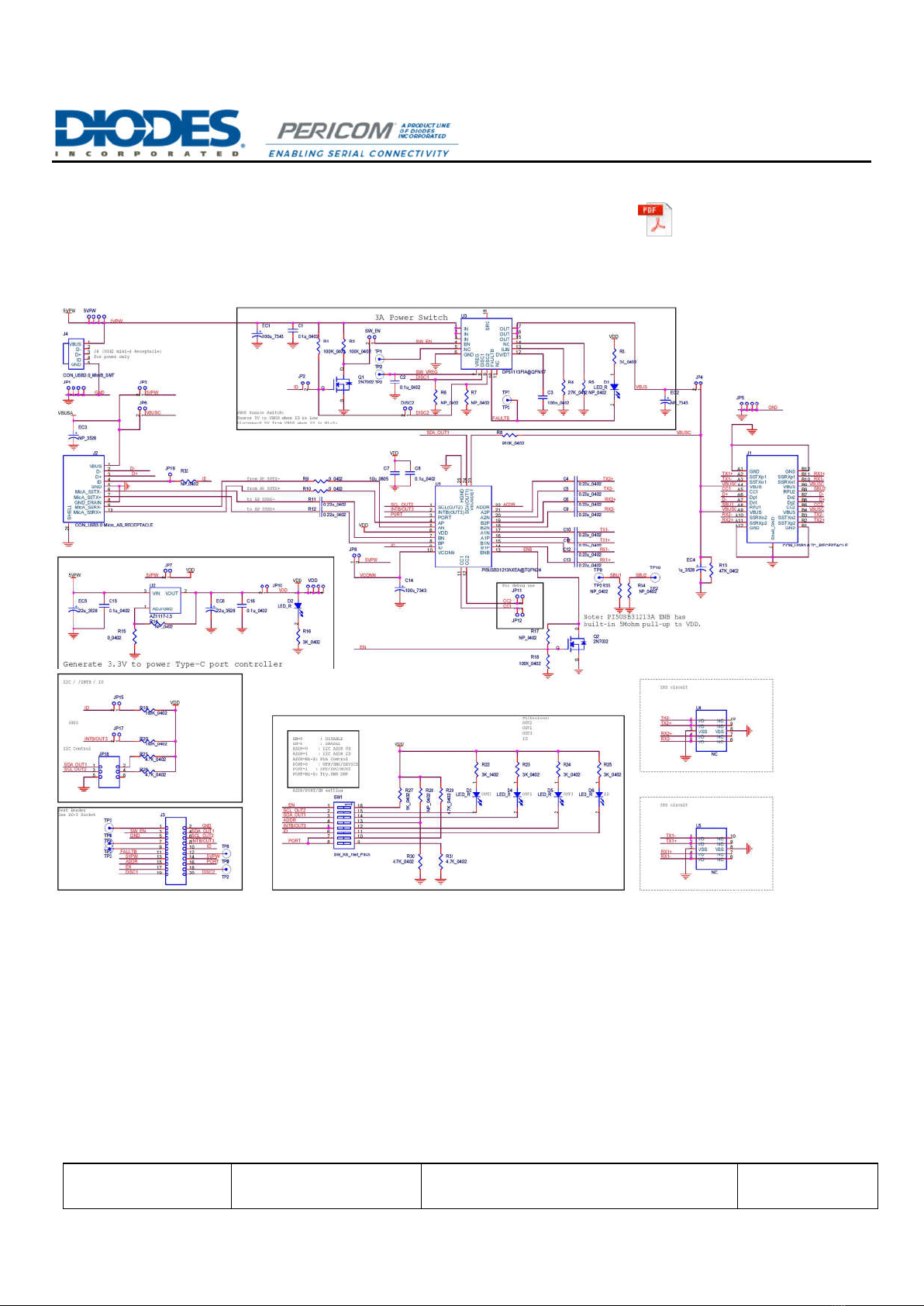
5 Appendix A: Demo Board Schematic
For clearer view of schematic diagram, please click the PDF file icon on the right.
PI5USB31213AXE
A_TYPE-C_EVB_REVB.pdf

ORIGINATE DATE
16 May, 2017
EDIT DATE
20 July, 2017 DOCUMENT-REV 1.1 PAGE
Page 13 of 14
AE Format Rev 1.2
Diodes Incorporated (Milpitas office)
1545 Barber Lane, Milpitas, CA 95035 U.S.A.
6 Appendix B: Demo Board Picture
ORIGINATE DATE
16 May, 2017
EDIT DATE
20 July, 2017 DOCUMENT-REV 1.1 PAGE
Page 14 of 14
AE Format Rev 1.2
Diodes Incorporated (Milpitas office)
1545 Barber Lane, Milpitas, CA 95035 U.S.A.
Revision History
Revision Date Description
1.0 16 May, 2017
Initial
1.1 20 July, 2017
Updated EVB schematic to ver.1.1
This manual suits for next models
1
Table of contents
Other Diodes Switch manuals


