Ecler DT4800 User manual

DT4800
DT6800
SERVICE MANUAL
THERMAL
STAND BY
OVERLOAD
THERMAL
STAND BY
OVERLOAD
64 5
2
CH2
1
0
3
8
10
9
7
CLIP
SIGNAL
4
2
CH1
1
0
3
56
8
10
9
7
CLIP
SIGNAL
ON
POWER
THERMAL
STAND BY
OVERLOAD
THERMAL
STAND BY
OVERLOAD
6
45
2
CH2
1
0
3
8
10
9
7
CLIP
SIGNAL
4
2
CH1
1
0
3
56
8
10
9
7
CLIP
SIGNAL
ON
POWER

SERVICE MANUAL DT4800 / DT6800
INDEX
-BLOCK DIAGRAM
-FUNCTIONING DESCRIPTION
-SCHEMATICS
-COMPONENTS LOCATION SCHEMA
-TECHNICAL CHARACTERISTICS
-WIRING DIAGRAM
-CONFIGURATION DIAGRAM
-MECHANICAL DIAGRAM
-PACKING DIAGRAM


52-0023-0100 EP05-02 Font Conmutada (Anglès).doc 1 of 2
POWER SUPPLY.
All of the explanations written in this document will be based on the schematics
shown on Figure 1. As it is not intended to generate a deep and precise description of its
performance, due to the complexity of the circuitry, this document will explain briefly the
basic principles on which this circuitry is based.
Figure1
AC INPUT EMC FILTER.
The first element found is a mains supply filter, made of a double-πstructure. This is
intended to avoid RF signal leakage (EMC) from the unit to other equipment, connected to
a common mains supply. The use of this kind of filters is quite usual in order to accomplish
European CE-label recommendations. It is a classical filter type, including two toroidal
cores, and both X- and Y-type capacitors.
author: J. Colomines date: 040308 project:
EP05-02
product:
DT6800/4800
E
C
LER approved:
num: 52..0023 version: 01.00
title:
FUNCTIONING DESCRIPTION
AC INPUT
EMC FILTER
PFC +
RECTIFIER FILTER RESONANT
HALF BRIDGE
OUTPUT
TRANSFORMER
PFC
CONTROL
POWER
SUPPLY
CONTROL
AUXILIAR
POWER
SUPPLY
AC MAINS
INPUT
OUTPUT FILTER
AND
RECTIFIER
Vaux+
STEP DOWN
Vaux -
REGULATOR
FAN
REGULATOR
FAN
AMP MODULE

52-0023-0100 EP05-02 Font Conmutada (Anglès).doc 2 of 2
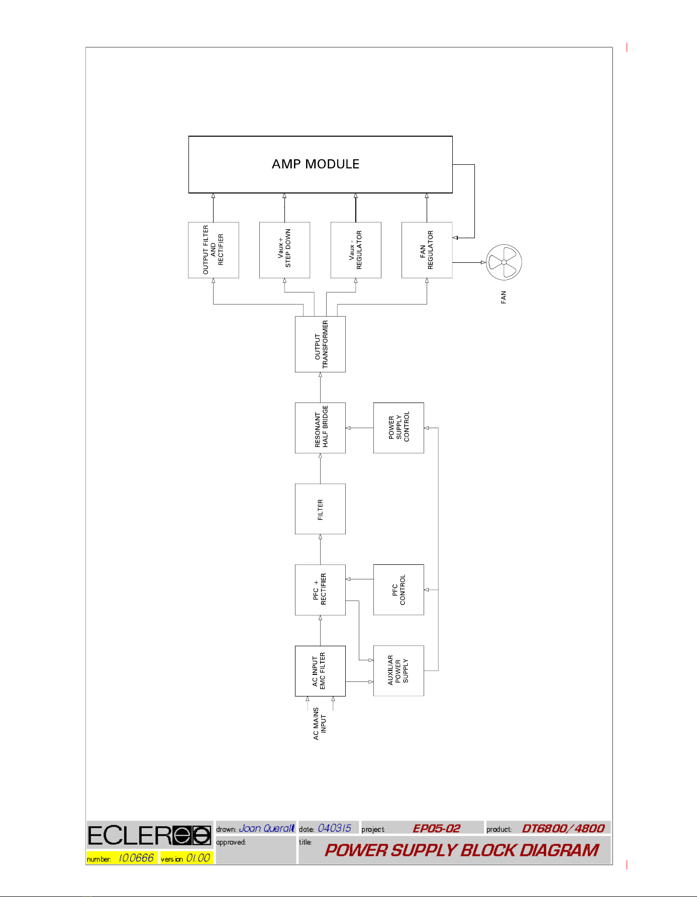
RECTIFIER, PFC AND FILTER.
These blocks are used to obtain a corrected Power consumption Factor value (phi).
This technique is used to reduce dramatically the harmonic contents of common domestic
mains signals before it reaches the power supply itself. The PFC (Power Factor Corrector)
reshapes its output mains waveform and produces a clear and smooth sine wave, in phase
with the waveform delivered through the mains supply. When this happens, the unit taps
power showing an external Power Factor (phi) almost equal to 1, thus essentially resistive.
The corrector is based on a “boost” circuit, which results to be the most appropriate for
this kind of active Power Factor Correction systems. By including a PFC in the power
supply, the mains wiring used can be thinner (less #AWG), the efficiency ratio increases,
and it also becomes easier to meet the European CE-label requirements.
PFC CONTROL.
Essentially, the controller consists on an analogical driver (a multiplier) which
multiplies the rectified input mains waveform with an error-related voltage value, obtained
from the output of the PFC circuit. The system tries constantly to match phases between
the consumed mains current sine wave and the mains voltage waveform.
AUXILIARY POWER SUPPLY.
This circuit delivers an additional power source to the control circuitry, which is
needed once the PFC starts to run. It is build around a 7815-type voltage regulator, fed
from a voltage multiplier which is connected to a secondary winging of the PFC’s toroidal
inductor. This supply has also to provide power to the Resonant Half Bridge control circuit,
which is explained next.
RESONANT HALF BRIDGE.
Resonant power supplies are conventionally shaped power supply structures (in this
case, a half-bridged supply), but in which particularly the internal current and voltages are
both tuned with the supply’s own running frequency, this is, it’s resonance rate. In our
case, the supply resonance is driven by a serial RLC circuit. As the current and voltage
flowing through R, L and C are in resonance, the switching losses are forced to be
minimal. The inductor of the RLC-cell is in fact the primary coil of the supply’s output
transformer. By this way, also the power loss at the semiconductors is very small, thus
reducing most of the circuitry’s EMI radiations.
OUTPUT TRANSFORMER.
Behind this point, the power supply can be considered like a conventional one. From
the output transformer’s both secondary coils, one delivering high power and the other low
voltage signals, all of the voltages required by the system will be obtained, once their
waveforms are rectified, filtered and stabilized when needed, using the most appropriate
circuitry for each function. In fact, this latest is the main target of our power supply.

52-0024-0100 EP05-02 Mòdul (Anglès).doc 1 of 4
POWER CIRCUITRY.
All of the explanations written in this document will be based on the schematics
shown on Figure 1. As it is not intended to generate a deep and precise description of its
performance, due to the complexity of the circuitry, this document will explain briefly the
basic principles on which this circuitry is based.
Figure1
INPUT STAGES.
Our usual balanced input stage is used, with a stacking output split, a low-pass filter
to avoid RF-noise humming on input signals, and a sub-sonic cut-off filter, internally ON-
OFF switchable, which allows to reject signals below the 20Hz constant cut off frequency.
author: J. Colomines date: 040312 project:
EP05-02
product:
DT6800/4800
E
C
LER approved:
num: 52.0024 version: 01.00
title:
FUNCTIONING DESCRIPTION
CURRENT
FEEDBACK
VOLTAGE
FEEDBACK
OUT+
CURRENT
FEEDBACK
+Vcc
ZOBEL
EMI
FILTER
TRIANGULAR
GENERATOR
MUTE
OUT+
OUT-
SIGNAL
PRESENT
INPUT
STACK
OUT
20Hz
FILTER
LOW PASS
FILTER
CURRENT
SENSE
CURRENT
FEEDBACK
PWM
CONTROL
THERMAL
PROBE
FAN
CONTROL
-Vref
+Vref
THERMAL
-Vref
VOL.
-Vref
CLIP
HIGH
FREQUENCY
FILTER
-Vref
OVER
ANTIALIASING
FILTER
CURRENT
SENSE
DETECTOR
R
R
+Vref
STANDBY
CIRCUIT
SUBSONIC
BANDPASS
PWM
CONTROL
DISABLE
MUTE
STANDBY
DISABLE DISABLE
AC LOSS
CIRCUIT
+Vref -Vref
DC OUT
adj.
ANTICLIP
CIRCUIT
FROM POWER
SUPPLY
OUT -
FEEDBACK
CIRCUIT
PULSE
CORRECTION
CIRCUIT
OSC.
COMMON
MODE
FILTER
DIFFERENTIAL
FILTER
DC OUT
CIRCUIT
ZOBEL PROTECTION
CIRCUIT
OUTPUT
CURRENT
LIMITER
PULSE
CORRECTION
CIRCUIT

52-0024-0100 EP05-02 Mòdul (Anglès).doc 2 of 4
ANTI-ALIASING FILTER.
The anti-aliasing filter, like on every digital equipment, is intended to allow signal
processing of input signal bandwidths just up to a half the system’s sample rate
(BWinput<1/2∙SR ), to avoid A/D conversion errors. Our system has an input signal
bandwidth of 35KHz, so the anti-aliasing cut-off frequency is slightly above this value.
THE PULSE WIDTH MODULATOR (PDM).
The amplifier runs on a 250KHz switching rate. This frequency is obtained from a
8MHz xtal, whose oscillation frequency is passed through a frequency divider, in order to
bring it back to a 500KHz. This allows to generate the 250KHz sawtooth wave, which will
be the carrier signal used by the PWM modulators.
The sawtooth waveform is obtained by processing this 500KHz square signal
through an integrator circuit, which produces a 250KHz 4Vpp sawtooth wave.
As the modulator used operates in BD-mode, this module has two PWM modulators,
which compare the same sawtooth carrier with each their own input signal, the modulating
audio+ and audio- signals, which in fact are the same but in phase opposition, obtained by
processing the module’s main input signal.
Each of this comparator is bound to a half power stage, and has two output nodes,
Q and Q’, which are the signals used to drive both upper and lower MoSFET’s. The driving
signals have a dead transition time, and operate between a maximum and a minimum pulse
width, in order to always avoid both upper and lower MoSFET’s to be conducting at the
same time in one single branch.
As already told, the power stage is build using a bridged structure, this is, each
branch has two half-bridges, and the module’s loading impedance hangs between their
outputs. This structure allows us to use an asymmetric power supply, which will have to
deliver just a half of the voltage needed if the same power level would have to be obtained
from each half-bridge module. Each half-bridge delivers a powerful PWM-signal, which,
once it is filtered, generates two opposed-phase low frequency AC signals.

52-0024-0100 EP05-02 Mòdul (Anglès).doc 3 of 4
OUTPUT FILTERS AND DC-PROTECTION.
The output filters, together with the DC-Out protection circuitry, are made of this
elements:
- A Differential mode filter.
- A Common mode filter.
- An EMI enhancement filter.
- A Zobel network-type compensating circuitry.
- The DC-Out protection circuitry.
The Differential mode-configured filter is used to clean high-frequency voltage from
the output signal. It is made of two capacitors and two induction coils. Such a filter is
placed on each of the half-bridge branches connected to the loudspeakers. Using this
filters, the 250KHz carrier signal is rejected, and only clear audio signal reaches the
loudspeakers.
The common mode-configured filter is also made of a capacitor and an inductor, and
is used to eliminate the carrier wave leakages from each output, as this noise signal has
the same polarity on each half-bridge output when referred to signal ground (0V).
The EMI-enhancement filter is placed nearby the final Speakon-type output
connection. This has to be done in order to avoid any kind of RF signal generated inside
the unit to be radiated into the environment.
The DC-Out protection circuitry is the same as the used in our analogue power
amplifiers. In case this circuit detects DC-levels, or very low frequencies (below 10Hz) with
more than 30V amplitude between the unit’s OUT+ and OUT- outputs, a TRIAC shorts the
output poles, avoiding the loudspeakers from being damaged by DC-signals.
FEEDBACK.
In order to ensure the stability of this modules, the correct feedback type has to be
chosen. When referring to PWM amplifiers, this feedback networks are more critical than
those used in analogue amplifiers. In our case, a double feedback system is being used:
sampling the amplifier’s output voltage after filtering, and the current flowing through one
of the differential filter coils.
The improvement obtained by using this second type of current-based feedback loop
consists in the possibility to reduce the output’s LC filter from a second to a first order
type of filter.

52-0024-0100 EP05-02 Mòdul (Anglès).doc 4 of 4
MUTE CIRCUITRY.
The Mute circuitry modifies the feedback system in order to improve stability when
the unit is turned on, this is, when the output modules suddenly receive the pulse trains,
just after the amplifier’s warm-up cycle. The mute circuitry damps the feedback’s adding
amplifier gain for a while, lasting a little bit more than the main unit’s standby cycle.
PROTECTIONS.
There are two main types of protections used in this modules: those who act when
a dangerous event is detected, and those who prevent from troubles by sampling the
amplifier’s output voltage and power.
Included in the first type of protections, there are:
- Protection against current overflow.
- Overheat protection.
- Run-up Protection (Standby cycle)
- Turnoff protection (AC Loss)
The second type of protections include:
- Anti-clipping protections.
- Temperature-controlled power damping system.
- Power damping, depending on the voltage measured on the Zobel-network’s
resistors.
- Cooling fan speed controlled by temperature.
- Progressive power increment after standby cycle.
All of the systems included in the first group act on the DISABLE control signal, as
this signal cuts off the upper MoSFET’s driving signal, on both half-bridges. See the
system’s block diagram.
The current overflow protection samples the current delivered by the power supply,
using a shunted sensor. When exceeding the safety limits, the voltage obtained from this
sensor trigs the current detector, which activates the DISABLE signal.
The second group of protections work all by correcting the VCA circuitry control
voltage. However, a special mention should be done on two of them. First of all, the unit’s
power damping as a function of the output frequency, in order to avoid the appearance of
excessive voltage and to keep the system stabilized even when the amplifier is clipping.
This is obtained by using a low-pass filter with a 3,5KHz -6dB cutoff frequency. Secondly,
the power level controlled by the voltage on the Zobel network’s resistor. This is used to
avoid this resistor from burning, even when the amplifier is processing high frequency
signals for longer periods of time.


PARTS LIST: PRINTED CIRCUIT 11.0862.07.01 (DT6800)
Code
Description
Reference
FCCE21100000
1000u/35
C101
FCCDH7010100
C1u/400V
C102
FCCDH7010100
C1u/400V
C103
FCCE25470000
470u/50
C104
FCCDH7010100
C1u/400V
C105
FCCC15004700
C4n7/300V Y2
C106
FCCC15004700
C4n7/300V Y2
C107
FCCE25047000
47u/50
C108
FCCC15101000
C100n
C109
FCCC15004700
C4n7/300V Y2
C110
FCCC15004700
C4n7/300V Y2
C111
FCCDK2001000
C1u/63V
C112
FCCDH7010100
C1u/400V
C113
FCCE25470000
470u/50
C114
FCCE25047000
47u/50
C115
FCCE25047000
47u/50
C116
FCCDH7010100
C1u/400V
C117
FCCE36022000
2200u/200
C118
FCCE36022000
2200u/200
C119
FCCE36022000
2200u/200
C120
FCCE36022000
2200u/200
C121
FCCE36022000
2200u/200
C122
FCCE36022000
2200u/200
C123
FCCDL5470000
C470n/1000V
C124
FCCCD5100000
C1n 2kV
C125
FCCCD4710000
C47p 3kV
C126
FCCCD4710000
C47p 3kV
C127
FCCE25220100
220u/50 ZL
C128
FCCC15101000
C100n
C129
FCCDM5390000
C390n/250V 383
C130
FCCDK2001000
C1u/63V
C131
FCCC15101000
C100n
C132
FCCC15101000
C100n
C133
FCCDM5390000
C390n/250V 383
C134
FCCC15004700
C4n7/300V Y2
C135
FCCE25220100
220u/50 ZL
C136
FCCCD5100000
C1n 2kV
C137
FCCCD5100000
C1n 2kV
C138
FCCE25220100
220u/50 ZL
C139
FCCE25470000
470u/50
C140
FCCE25470000
470u/50
C141
FCCE25220100
220u/50 ZL
C142
FCCE25220100
220u/50 ZL
C143
FCCE35004700
47u/200
C144
FCCC15101000
C100n
C145
FCCDK1010000
C10n
C146
FCCE25220100
220u/50 ZL
C147
FCCC15101000
C100n
C148
FCCE20022000
22u/35
C149
FCCE25010000
10u/50
C150
FCCDK1470000
C470n
C151
FCCE36022000
2200u/200
C152
FCCC12680000
C680p
C153
FCCE36022000
2200u/200
C154
FCCE25220100
220u/50 ZL
C155
FCCDK2001000
C1u/63V
C156
40-0097-0103 EP05-02A DT6800.xls 1 of 7

PARTS LIST: PRINTED CIRCUIT 11.0862.07.01 (DT6800)
Code
Description
Reference
FCCDK2001000
C1u/63V
C157
FCCE36022000
2200u/200
C158
FCCE36022000
2200u/200
C159
FCCDK1010000
C10n
C160
FCCDK1010000
C10n
C161
FCPERL255000
Cer. Bead
CB101
FCPERL255000
Cer. Bead
CB102
FCPERL255000
Cer. Bead
CB103
FCPERL255000
Cer. Bead
CB104
FCPERL255000
Cer. Bead
CB105
FCPERL255000
Cer. Bead
CB106
FCPERL255000
Cer. Bead
CB107
FCPERL255000
Cer. Bead
CB108
FCPERL255000
Cer. Bead
CB109
FCPERL255000
Cer. Bead
CB110
FCPERL255000
Cer. Bead
CB111
FCPERL255000
Cer. Bead
CB112
FCPERL255000
Cer. Bead
CB113
FCPERL255000
Cer. Bead
CB114
FCPERL255000
Cer. Bead
CB115
FCPERL255000
Cer. Bead
CB116
FCPERL255000
Cer. Bead
CB117
FCPERL255000
Cer. Bead
CB118
FCPERL255000
Cer. Bead
CB119
FCPERL255000
Cer. Bead
CB120
FCPERL255000
Cer. Bead
CB121
FCPERL255000
Cer. Bead
CB122
FCPERL255000
Cer. Bead
CB123
FCPERL255000
Cer. Bead
CB124
FCPERL255000
Cer. Bead
CB125
FCPERL255000
Cer. Bead
CB126
FCPERL255000
Cer. Bead
CB127
FCPERL255000
Cer. Bead
CB128
FCPERL255000
Cer. Bead
CB129
FCPERL255000
Cer. Bead
CB130
FCPERL255000
Cer. Bead
CB131
FCPERL255000
Cer. Bead
CB132
FCCI00862000
Printed Board 11.0862
CI101
FCDD14007000
1N4007
D101
FCDD10180000
Z18V/1
D102
FCDD14007000
1N4007
D103
FCDD14007000
1N4007
D104
FCREC5006000
FB5006
D105
FCDD14007000
1N4007
D106
FCDDMUR14000
MUR140
D107
FCDDMUR44000
MUR460
D108
FCDDMUR44000
MUR460
D109
FCDDMUR14000
MUR140
D110
FCDD50600000
RHRG5060
D111
FCDD50600000
RHRG5060
D112
FCDDBAT42000
BAT42
D113
FCDDBAT42000
BAT42
D114
FCDDBAT42000
BAT42
D115
FCDDBAT42000
BAT42
D116
FCDDBAT42000
BAT42
D117
FCDDBAT42000
BAT42
D118
40-0097-0103 EP05-02A DT6800.xls 2 of 7
Other manuals for DT4800
1
This manual suits for next models
1
Table of contents
Other Ecler Amplifier manuals

Ecler
Ecler MPA280 User manual

Ecler
Ecler eCA120HZ User manual

Ecler
Ecler CA200z User manual

Ecler
Ecler DPA2000 User manual

Ecler
Ecler Dante VIDA-24Q User manual

Ecler
Ecler Ampack2-20 User manual

Ecler
Ecler CA40 User manual

Ecler
Ecler eHSA SERIES User manual

Ecler
Ecler DVA 1-5c User manual

Ecler
Ecler VEO-SPH44 User manual

Ecler
Ecler HZA4-70F User manual

Ecler
Ecler VIDA Series User manual

Ecler
Ecler eHSA2-250 User manual

Ecler
Ecler CA40 User manual

Ecler
Ecler VEO-SPH48 User manual

Ecler
Ecler DPA600 User manual

Ecler
Ecler APA1400 User manual

Ecler
Ecler XPA20000 User manual

Ecler
Ecler eCA120 User manual

Ecler
Ecler LPA6000 User manual